 | –≠–ª–µ–∫—Ç—Ä–æ–Ω–Ω—ã–π –∫–æ–º–ø–æ–Ω–µ–Ω—Ç: SDB10S30 | –°–∫–∞—á–∞—Ç—å:  PDF PDF  ZIP ZIP |

2001-12-04
Page 1
SDP10S30, SDB10S30
SDT10S30
Preliminary data
Silicon Carbide Schottky Diode
Revolutionary semiconductor
material - Silicon Carbide
Switching behavior benchmark
No reverse recovery
No temperature influence on
the switching behavior
No forward recovery
Product Summary
V
RRM
300
V
Q
c
23
nC
I
F
10
A
P-TO220-2-2.
P-TO220-3-1.
P-TO220-3.SMD
Pin 1
PIN 2
PIN 3
n.c.
C
A
n.c.
C
A
Marking
D10S30
D10S30
D10S30
Type
Package
Ordering Code
SDP10S30
P-TO220-3-1.
Q67040-S4372
SDB10S30
P-TO220-3.SMD Q67040-S4373
SDT10S30
P-TO220-2-2.
Q67040-S4447
C
A
Maximum Ratings,at T
j
= 25 ∞C, unless otherwise specified
Parameter
Symbol
Value
Unit
Continuous forward current,
T
C
=100∞C
I
F
10
A
RMS forward current
,
f
=50Hz
I
FRMS
14
Surge non repetitive forward current, sine halfwave
T
C
=25∞C, t
p
=10ms
I
FSM
36
Repetitive peak forward current
T
j
=150∞C, T
C
=100∞C, D=0.1
I
FRM
45
Non repetitive peak forward current
t
p
=10µs, T
C
=25∞C
I
FMAX
100
i
2
t value
,
T
C
=25∞C, t
p
=10ms
i
2
dt
6.5
A≤s
Repetitive peak reverse voltage
V
RRM
300
V
Surge peak reverse voltage
V
RSM
300
Power dissipation
,
T
C
=25∞C
P
tot
65
W
Operating and storage temperature
T
j ,
T
stg
-55... +175
∞C

2001-12-04
Page 2
SDP10S30, SDB10S30
SDT10S30
Preliminary data
Thermal Characteristics
Parameter
Symbol
Values
Unit
min.
typ.
max.
Characteristics
Thermal resistance, junction - case
R
thJC
-
-
2.3
K/W
SMD version, device on PCB:
P-TO263-3-2: @ min. footprint
P-TO263-3-2: @ 6 cm
2
cooling area
1)
R
thJA
-
-
-
35
62
-
Electrical Characteristics, at T
j
= 25 ∞C, unless otherwise specified
Parameter
Symbol
Values
Unit
min.
typ.
max.
Static Characteristics
Diode forward voltage
I
F
=10A, T
j
=25∞C
I
F
=10A, T
j
=150∞C
V
F
-
-
1.5
1.5
1.7
1.9
V
Reverse current
V
R
=300V, T
j
=25∞C
V
R
=300V, T
j
=150∞C
I
R
-
-
15
20
200
1000
µA
1Device on 40mm*40mm*1.5mm epoxy PCB FR4 with 6cm≤ (one layer, 70 µm thick) copper area for drain
connection. PCB is vertical without blown air.

2001-12-04
Page 3
SDP10S30, SDB10S30
SDT10S30
Preliminary data
Electrical Characteristics,at T
j
= 25 ∞C, unless otherwise specified
Parameter
Symbol
Values
Unit
min.
typ.
max.
AC Characteristics
Total capacitive charge
1)
V
R
=200V, I
F
=10A, di
F
/dt
=-200A/µs, T
j
=150∞C
Q
c
-
23
-
nC
Switching time
2)
V
R
=200V, I
F
=10A, di
F
/dt
=-200A/µs, T
j
=150∞C
t
rr
-
n.a.
-
ns
Total capacitance
V
R
=0V, T
C
=25∞C, f=1MHz
V
R
=150V, T
C
=25∞C, f=1MHz
V
R
=300V, T
C
=25∞C, f=1MHz
C
-
-
-
600
55
40
-
-
-
pF
2001-12-04
Page 4
SDP10S30, SDB10S30
SDT10S30
Preliminary data
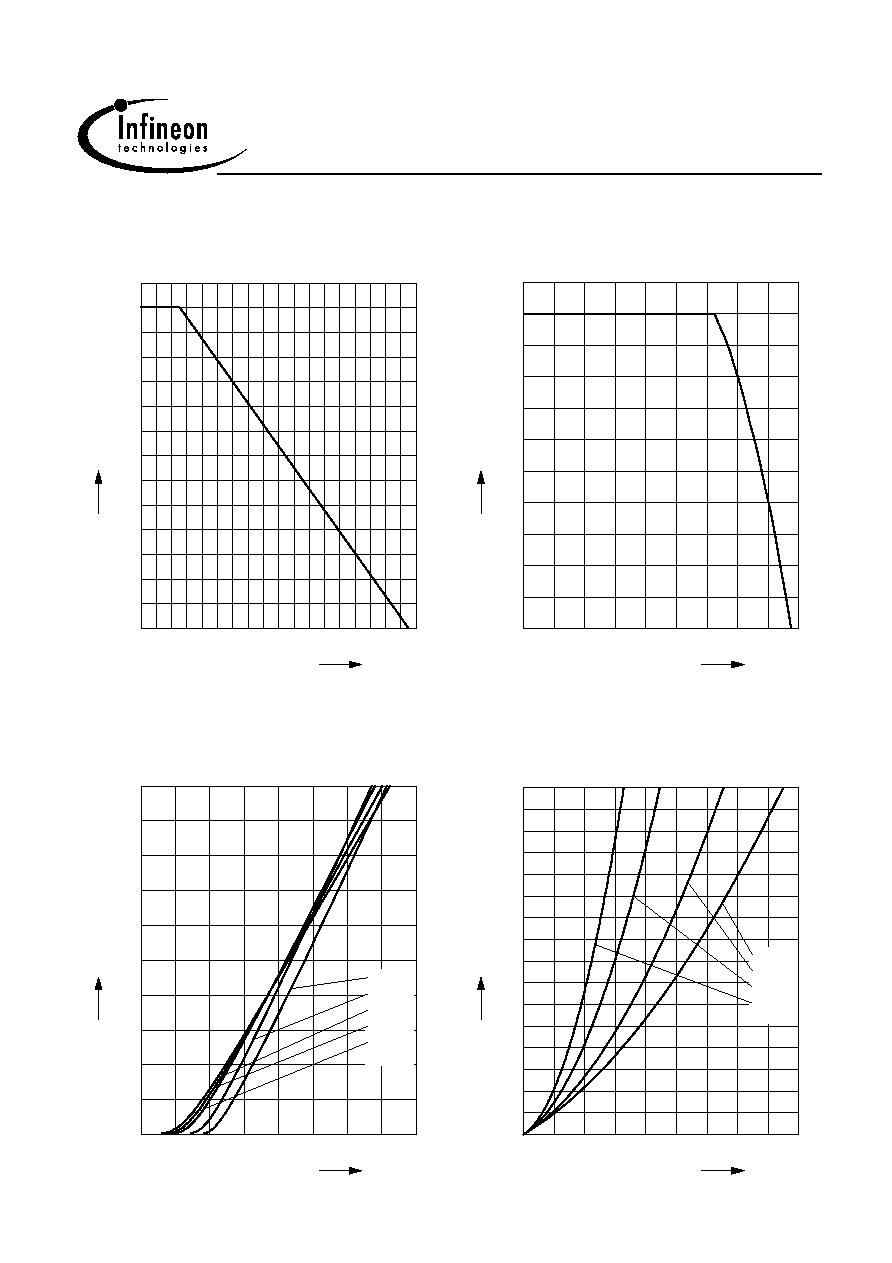
1 Power dissipation
P
tot
= f (T
C
)
0
20
40
60
80
100 120 140
∞C
180
T
C
0
5
10
15
20
25
30
35
40
45
50
55
60
W
70
P
tot
2 Diode forward current
I
F
= f (T
C
)
parameter: T
j
175 ∞C
0
20
40
60
80
100 120 140
∞C
180
T
C
0
1
2
3
4
5
6
7
8
9
A
11
I
F
4 Typ. forward power dissipation vs.
average forward current
P
F(AV)=f(I
F
)
T
C
=100∞C, d = t
p
/T
0
2
4
6
8
10
12
14
A
18
I
F(AV)
0
4
8
12
16
20
24
W
32
P
F(AV)
d=1
d=0.5
d=0.2
d=0.1
3 Typ. forward characteristic
I
F
= f (V
F
)
parameter: Tj , t
p
= 350 µs
0.6
0.8
1
1.2
1.4
1.6
1.8
V
2.2
V
F
0
2
4
6
8
10
12
14
16
A
20
I
F
-40∞C
25∞C
100∞C
125∞C
150∞C

2001-12-04
Page 5
SDP10S30, SDB10S30
SDT10S30
Preliminary data
5 Typ. reverse current vs. reverse voltage
I
R
=f(V
R
)
50
100
150
200
V
300
V
R
-4
10
-3
10
-2
10
-1
10
0
10
1
10
2
10
µA
I
R
150∞C
125∞C
100∞C
25∞C
6 Transient thermal impedance
Z
thJC
= f (t
p
)
parameter : D = t
p
/T
10
-7
10
-6
10
-5
10
-4
10
-3
10
-2
10
0
s
t
p
-4
10
-3
10
-2
10
-1
10
0
10
1
10
K/W
SDP10S30
Z
thJC
single pulse
0.01
0.02
0.05
0.10
0.20
D = 0.50
7 Typ. capacitance vs. reverse voltage
C= f(V
R
)
parameter: T
C
= 25 ∞C, f = 1 MHz
10
0
10
1
10
2
10
3
V
V
R
0
50
100
150
200
250
300
350
pF
450
C
8 Typ. C stored energy
E
C
=f(V
R
)
0
50
100
150
200
V
300
V
R
0
0.5
1
1.5
µJ
2.5
E
C