 | –≠–ª–µ–∫—Ç—Ä–æ–Ω–Ω—ã–π –∫–æ–º–ø–æ–Ω–µ–Ω—Ç: SGP20N60 | –°–∫–∞—á–∞—Ç—å:  PDF PDF  ZIP ZIP |

SGP20N60
SGB20N60, SGW20N60
1
Mar-00
Fast S-IGBT in NPT-technology
G
C
E
∑
75% lower E
off
compared to previous generation combined with
low conduction losses
∑
Short circuit withstand time ≠ 10
µ
s
∑
Designed for:
- Motor controls
- Inverter
∑
NPT-Technology for 600V applications offers:
- very tight parameter distribution
- high ruggedness, temperature stable behaviour
- parallel switching capability
Type
V
CE
I
C
V
CE(sat)
T
j
Package
Ordering Code
SGP20N60
SGB20N60
SGW20N60
600V
20A
2.4V
150
∞
C
TO-220AB
TO-263AB
TO-247AC
Q67041-A4712-A2
Q67041-A4712-A4
Q67040-S4236
Maximum Ratings
Parameter
Symbol
Value
Unit
Collector-emitter voltage
V
C E
600
V
DC collector current
T
C
= 25
∞
C
T
C
= 100
∞
C
I
C
40
20
Pulsed collector current, t
p
limited by T
jmax
I
C p u l s
80
Turn off safe operating area
V
CE
600V, T
j
150
∞
C
-
80
A
Gate-emitter voltage
V
G E
±
20
V
Avalanche energy, single pulse
I
C
= 20 A, V
CC
= 50 V, R
GE
= 25
,
start at T
j
= 25
∞
C
E
A S
115
mJ
Short circuit withstand time
1)
V
GE
= 15V, V
CC
600V, T
j
150
∞
C
t
S C
10
µ
s
Power dissipation
T
C
= 25
∞
C
P
t o t
179
W
Operating junction and storage temperature
T
j
, T
s t g
-55...+150
∞
C
1)
Allowed number of short circuits: <1000; time between short circuits: >1s.

SGP20N60
SGB20N60, SGW20N60
2
Mar-00
Thermal Resistance
Parameter
Symbol
Conditions
Max. Value
Unit
Characteristic
IGBT thermal resistance,
junction ≠ case
R
t h J C
0.7
Thermal resistance,
junction ≠ ambient
R
t h J A
TO-247AC
40
K/W
Electrical Characteristic, at T
j
= 25
∞
C, unless otherwise specified
Value
Parameter
Symbol
Conditions
min.
Typ.
max.
Unit
Static Characteristic
Collector-emitter breakdown voltage
V
( B R ) C E S
V
G E
=0V, I
C
=500
µ
A
600
-
-
Collector-emitter saturation voltage
V
C E ( s a t )
V
G E
= 15V, I
C
=20A
T
j
=25
∞
C
T
j
=150
∞
C
1.7
-
2
2.4
2.4
2.9
Gate-emitter threshold voltage
V
G E ( t h )
I
C
=700
µ
A,V
C E
=V
G E
3
4
5
V
Zero gate voltage collector current
I
C E S
V
C E
=600V,V
G E
=0V
T
j
=25
∞
C
T
j
=150
∞
C
-
-
-
-
40
2500
µ
A
Gate-emitter leakage current
I
G E S
V
C E
=0V,V
G E
=20V
-
-
100
nA
Transconductance
g
f s
V
C E
=20V, I
C
=20A
-
14
-
S
Dynamic Characteristic
Input capacitance
C
i s s
-
1100
1320
Output capacitance
C
o s s
-
107
128
Reverse transfer capacitance
C
r s s
V
C E
=25V,
V
G E
=0V,
f=1MHz
-
63
76
pF
Gate charge
Q
G a t e
V
C C
=480V, I
C
=20A
V
G E
=15V
-
100
130
nC
Internal emitter inductance
measured 5mm (0.197 in.) from case
L
E
T O-247AC
Feh ler!
Verw eisqu elle
konnt e nicht
gefun den
w erd en.
-
-
7
13
-
nH
Short circuit collector current
1)
I
C ( S C )
V
G E
=15V,t
S C
10
µ
s
V
C C
600V,
T
j
150
∞
C
-
200
-
A
1)
Allowed number of short circuits: <1000; time between short circuits: >1s.

SGP20N60
SGB20N60, SGW20N60
3
Mar-00
Switching Characteristic, Inductive Load, at T
j
=25
∞
C
Value
Parameter
Symbol
Conditions
min.
typ.
max.
Unit
IGBT Characteristic
Turn-on delay time
t
d ( o n )
-
36
46
Rise time
t
r
-
30
36
Turn-off delay time
t
d ( o f f )
-
225
270
Fall time
t
f
-
54
65
ns
Turn-on energy
E
o n
-
0.44
0.53
Turn-off energy
E
o f f
-
0.33
0.43
Total switching energy
E
t s
T
j
=25
∞
C,
V
C C
=400V,I
C
=20A,
V
G E
=0/15V,
R
G
=16
,
Energy losses include
"tail" and diode
reverse recovery.
-
0.77
0.96
mJ
Switching Characteristic, Inductive Load, at T
j
=150
∞
C
Value
Parameter
Symbol
Conditions
min.
typ.
max.
Unit
IGBT Characteristic
Turn-on delay time
t
d ( o n )
-
36
46
Rise time
t
r
-
30
36
Turn-off delay time
t
d ( o f f )
-
250
300
Fall time
t
f
-
63
76
ns
Turn-on energy
E
o n
-
0.67
0.81
Turn-off energy
E
o f f
-
0.49
0.64
Total switching energy
E
t s
T
j
=150
∞
C
V
C C
=400V,
I
C
=20A,
V
G E
=0/15V,
R
G
=16
Energy losses include
"tail" and diode
reverse recovery.
-
1.12
1.45
mJ

SGP20N60
SGB20N60, SGW20N60
4
Mar-00
I
C
,
COLLE
CT
OR CURRE
N
T
10Hz
100Hz
1kHz
10kHz
100kHz
0A
10A
20A
30A
40A
50A
60A
70A
80A
90A
100A
110A
T
C
=110∞C
T
C
=80∞C
I
C
,
COLLE
CT
OR CURRE
N
T
1V
10V
100V
1000V
0.1A
1A
10A
100A
DC
1ms
200
µ
s
50
µ
s
15
µ
s
t
p
=4
µ
s
f,
SWITCHING FREQUENCY
V
CE
,
COLLECTOR
-
EMITTER VOLTAGE
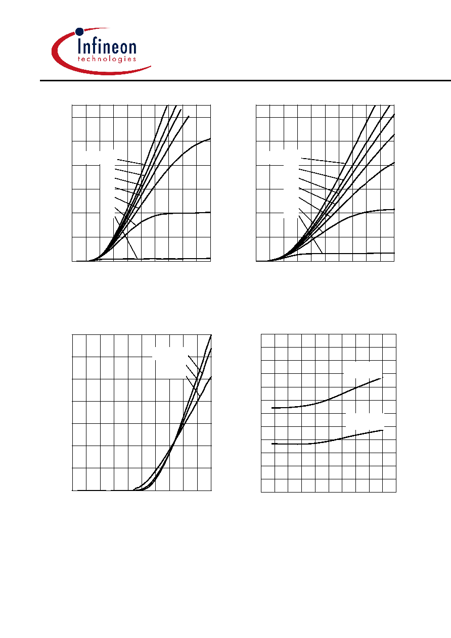
Figure 1. Collector current as a function of
switching frequency
(T
j
150
∞
C, D = 0.5, V
CE
= 400V,
V
GE
= 0/+15V, R
G
= 16
)
Figure 2. Safe operating area
(D = 0, T
C
= 25
∞
C, T
j
150
∞
C)
P
tot
,
PO
W
E
R
D
I
SS
IP
AT
IO
N
25∞C
50∞C
75∞C
100∞C
125∞C
0W
20W
40W
60W
80W
100W
120W
140W
160W
180W
200W
I
C
,
COLLE
CT
OR CURRE
NT
25∞C
50∞C
75∞C
100∞C
125∞C
0A
10A
20A
30A
40A
50A
T
C
,
CASE TEMPERATURE
T
C
,
CASE TEMPERATURE
Figure 3. Power dissipation as a function
of case temperature
(T
j
150
∞
C)
Figure 4. Collector current as a function of
case temperature
(V
GE
15V, T
j
150
∞
C)
I
c
I
c
SGP20N60
SGB20N60, SGW20N60
5
Mar-00
I
C
,
COLLE
CT
OR CURRE
N
T
0V
1V
2V
3V
4V
5V
0A
10A
20A
30A
40A
50A
60A
15V
13V
11V
9V
7V
5V
V
GE
=20V
I
C
,
COLLE
CT
OR CURRE
N
T
0V
1V
2V
3V
4V
5V
0A
10A
20A
30A
40A
50A
60A
15V
13V
11V
9V
7V
5V
V
GE
=20V
V
CE
,
COLLECTOR
-
EMITTER VOLTAGE
V
CE
,
COLLECTOR
-
EMITTER VOLTAGE
Figure 5. Typical output characteristics
(T
j
= 25
∞
C)
Figure 6. Typical output characteristics
(T
j
= 150
∞
C)
I
C
,
COLLE
CT
OR CURRE
N
T
0V
2V
4V
6V
8V
10V
0A
10A
20A
30A
40A
50A
60A
70A
-55∞C
+150∞C
T
j
=+25∞C
V
CE(sat)
,
COLLE
CT
OR
-
EM
ITT
E
R
SATU
R
ATI
O
N
VO
L
T
AG
E
-50∞C
0∞C
50∞C
100∞C 150∞C
1.0V
1.5V
2.0V
2.5V
3.0V
3.5V
4.0V
V
GE
,
GATE
-
EMITTER VOLTAGE
T
j
,
JUNCTION TEMPERATURE
Figure 7. Typical transfer characteristics
(V
CE
= 10V)
Figure 8. Typical collector-emitter
saturation voltage as a function of junction
temperature
(V
GE
= 15V)
I
C
= 20A
I
C
= 40A