 | ÐлекÑÑоннÑй компоненÑ: SMBT3904 | СкаÑаÑÑ:  PDF PDF  ZIP ZIP |
Äîêóìåíòàöèÿ è îïèñàíèÿ www.docs.chipfind.ru
SMBT3904/ MMBT3904
1
Feb-18-2002
NPN Silicon Switching Transistor
High DC current gain: 0.1mA to 100mA
Low collector-emitter saturation voltage
Complementary type: SMBT3906 (PNP)
1
2
3
VPS05161
Type
Marking
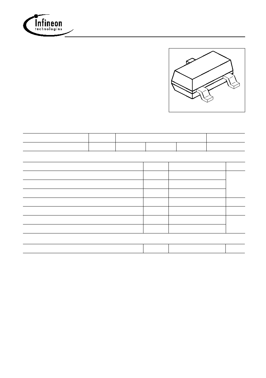
Pin Configuration
Package
SMBT3904/ MMBT3904
s1A
1 = B
2 = E
3 = C
SOT23
Maximum Ratings
Parameter
Symbol
Value
Unit
Collector-emitter voltage
V
CEO
40
V
Collector-base voltage
V
CBO
60
Emitter-base voltage
V
EBO
6
DC collector current
I
C
200
mA
Total power dissipation
,
T
S
= 69 °C
P
tot
330
mW
Junction temperature
T
j
150
°C
Storage temperature
T
stg
-65 ... 150
Thermal Resistance
Junction - soldering point
1)
R
thJS
245
K/W
1For calculation of R
thJA
please refer to Application Note Thermal Resistance

SMBT3904/ MMBT3904
2
Feb-18-2002
Electrical Characteristics at T
A
= 25°C, unless otherwise specified.
Parameter
Symbol
Values
Unit
min.
typ.
max.
DC Characteristics
Collector-emitter breakdown voltage
I
C
= 1 mA,
I
B
= 0
V
(BR)CEO
40
-
-
V
Collector-base breakdown voltage
I
C
= 10 µA,
I
E
= 0
V
(BR)CBO
60
-
-
Emitter-base breakdown voltage
I
E
= 10 µA,
I
C
= 0
V
(BR)EBO
6
-
-
Collector cutoff current
V
CB
= 30 V,
I
E
= 0
I
CBO
-
-
50
nA
DC current gain 1)
I
C
= 100 µA,
V
CE
= 1 V
I
C
= 1 mA,
V
CE
= 1 V
I
C
= 10 mA,
V
CE
= 1 V
I
C
= 50 mA,
V
CE
= 1 V
I
C
= 100 mA,
V
CE
= 1 V
h
FE
40
70
100
60
30
-
-
-
-
-
-
-
300
-
-
-
Collector-emitter saturation voltage1)
I
C
= 10 mA,
I
B
= 1 mA
I
C
= 50 mA,
I
B
= 5 mA
V
CEsat
-
-
-
-
0.2
0.3
V
Base-emitter saturation voltage 1)
I
C
= 10 mA,
I
B
= 1 mA
I
C
= 50 mA,
I
B
= 5 mA
V
BEsat
0.65
-
-
-
0.85
0.95
1) Pulse test: t
=
300
µ
s, D = 2%

SMBT3904/ MMBT3904
3
Feb-18-2002
Electrical Characteristics at T
A
= 25°C, unless otherwise specified.
Parameter
Symbol
Values
Unit
min.
typ.
max.
AC Characteristics
Transition frequency
I
C
= 10 mA,
V
CE
= 20 V,
f
= 100 MHz
f
T
300
-
-
MHz
Collector-base capacitance
V
CB
= 5 V,
f
= 1 MHz
C
cb
-
-
4
pF
Emitter-base capacitance
V
EB
= 0.5 V,
f
= 1 MHz
C
eb
-
-
8
Noise figure
I
C
= 100 µA,
V
CE
= 5 V,
R
S
= 1
k
,
f
= 1 kHz,
f
= 200
Hz
F
-
-
5
dB
Short-circuit input impedance
I
C
= 1 mA,
V
CE
= 10 V,
f
= 1 kHz
h
11e
1
-
10
k
Open-circuit reverse voltage transf.ratio
I
C
= 1 mA,
V
CE
= 10 V,
f
= 1 kHz
h
12e
0.5
-
8
10
-4
Short-circuit forward current transf.ratio
I
C
= 1 mA,
V
CE
= 10 V,
f
= 1 kHz
h
21e
100
400
-
-
Open-circuit output admittance
I
C
= 1 mA,
V
CE
= 10 V,
f
= 1 kHz
h
22e
1
-
40
S
Delay time
V
CC
= 3 V,
I
C
= 10 mA,
I
B1
= 1 mA,
V
BE(off)
= 0.5 V
t
d
-
-
35
ns
Rise time
V
CC
= 3 V,
I
C
= 10 mA,
I
B1
= 1 mA,
V
BE(off)
= 0.5 V
t
r
-
-
35
Storage time
V
CC
= 3 V,
I
C
= 10 mA, I
B1
=I
B2
= 1mA
t
stg
-
-
200
Fall time
V
CC
= 3 V,
I
C
= 10 mA, I
B1
=I
B2
=
1mA
t
f
-
-
50
SMBT3904/ MMBT3904
4
Feb-18-2002
Test circuits
Delay and rise tim
e
EHN00061
275
10 k
+3.0 V
0
-0.5 V
<4.0 pF
C
+10.9 V
D = 2%
300 ns
<1.0 ns
Storage and fall time
EHN00062
275
10
+3.0 V
0
-9.1
<4.0 pF
C
+10.9 V
D = 2%
1N916
<1.0
t
1
µ
s
500
10 t
1
V
k
ns
< <
SMBT3904/ MMBT3904
5
Feb-18-2002
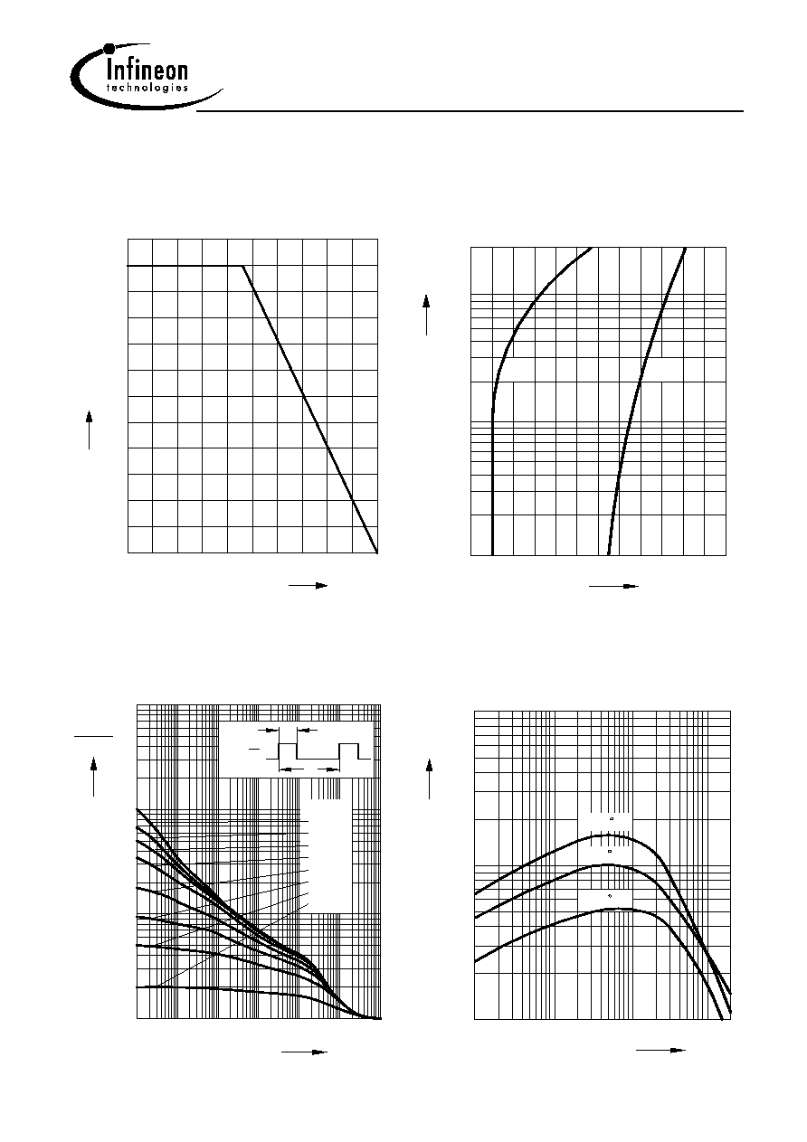
Saturation voltage
I
C
= f (V
BEsat
, V
CEsat
)
h
FE
= 10
EHP00756
2
0
V
BE sat
C
10
1
10
0
5
V
mA
0.2
0.4
0.6
0.8
1.0
1.2
CE sat
V
,
5
10
2
V
BE
V
CE
Total power dissipation
P
tot
= f(T
S
)
0
15
30
45
60
75
90 105 120
°C
150
T
S
0
30
60
90
120
150
180
210
240
270
300
mW
360
P
tot
Permissible pulse load
P
totmax
/ P
totDC
= f (t
p
)
10
EHP00935
-6
0
10
5
D =
5
10
1
10
2
3
10
10
-5
10
-4
10
-3
10
-2
10
0
s
0
0.005
0.01
0.02
0.05
0.1
0.2
0.5
-1
10
tot max
tot
P
DC
P
p
t
t
p
=
D
T
t
p
T
DC current gain
h
FE
= f (I
C
)
V
CE
= 10V, normalized
EHP00765
10
10
mA
h
C
5
FE
10
1
0
10
-1
5
10
10
10
-1
0
1
2
125 C
25 C
-55 C
5
5
2