Äîêóìåíòàöèÿ è îïèñàíèÿ www.docs.chipfind.ru
2003-10-08
Page 1
SPP20N60C3, SPB20N60C3
SPI20N60C3, SPA20N60C3
Final data
Cool MOSTM
Power Transistor
V
DS
@
T
jmax
650
V
R
DS(on)
0.19
I
D
20.7
A
Feature
·
New revolutionary high voltage technology
·
Worldwide best R
DS(on)
in TO 220
·
Ultra low gate charge
·
Periodic avalanche rated
·
Extreme dv/dt rated
·
High peak current capability
·
Improved transconductance
·
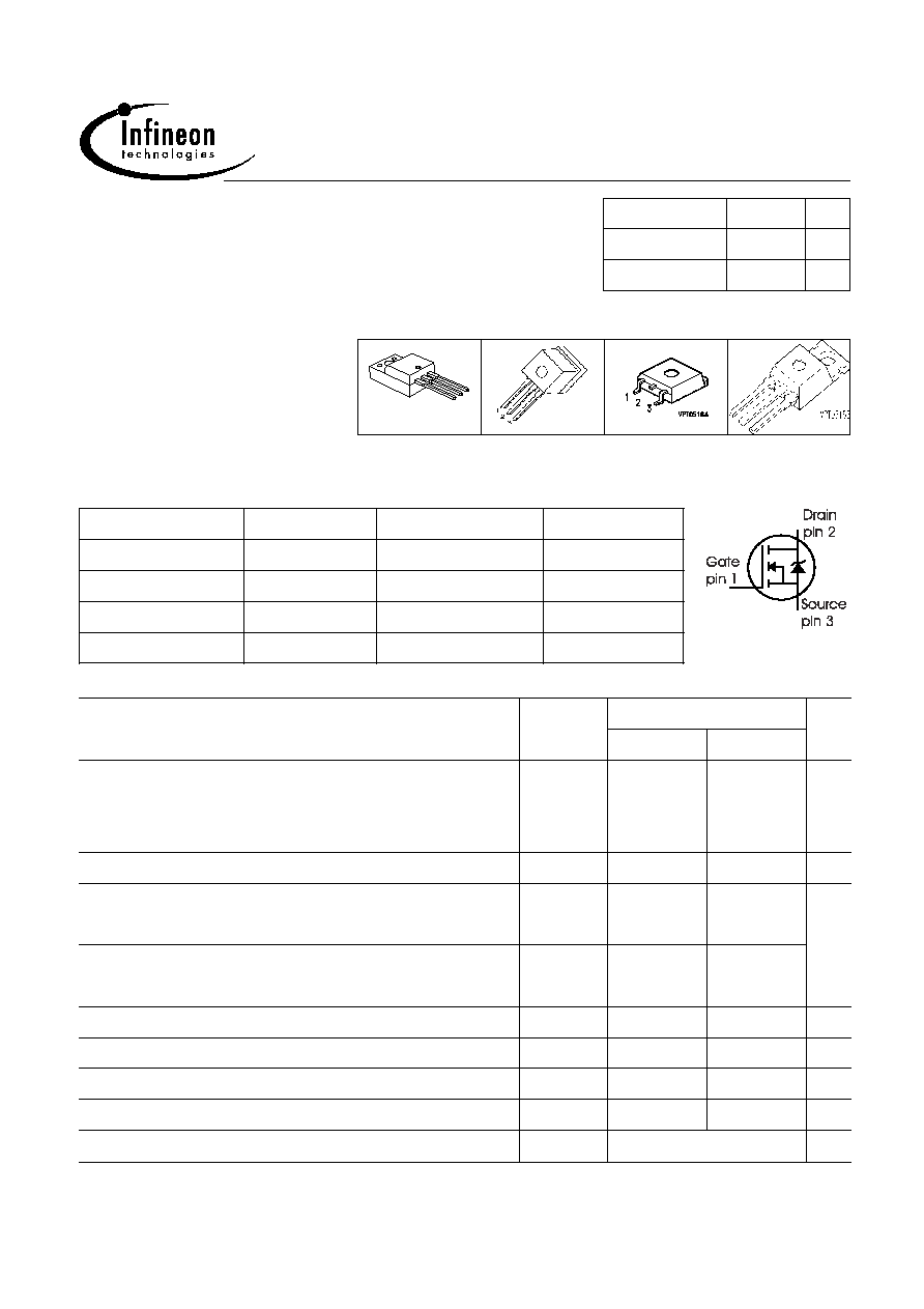
P-TO-220-3-31: Fully isolated package (2500 VAC; 1 minute)
P-TO262-3-1
P-TO263-3-2
P-TO220-3-31
P-TO220-3-1
P-TO220-3-31
1
2
3
Marking
20N60C3
20N60C3
20N60C3
20N60C3
Type
Package
Ordering Code
SPP20N60C3
P-TO220-3-1
Q67040-S4398
SPB20N60C3
P-TO263-3-2
Q67040-S4397
SPI20N60C3
P-TO262-3-1
Q67040-S4550
SPA20N60C3
P-TO220-3-31 Q67040-S4410
Maximum Ratings
Parameter
Symbol
Value
Unit
SPA
Continuous drain current
T
C
= 25 °C
T
C
= 100 °C
I
D
20.7
13.1
20.7
1)
13.1
1)
A
Pulsed drain current,
t
p
limited by
T
jmax
I
D puls
62.1
62.1
A
Avalanche energy, single pulse
I
D
=10A,
V
DD
=50V
E
AS
690
690
mJ
Avalanche energy, repetitive t
AR
limited by
T
jmax
2)
I
D
=20A,
V
DD
=50V
E
AR
1
1
Avalanche current, repetitive t
AR
limited by
T
jmax
I
AR
20
20
A
Gate source voltage static
V
GS
±20
±20
V
Gate source voltage AC (f >1Hz)
V
GS
±
30
±
30
Power dissipation,
T
C
= 25°C
P
tot
208
34.5
W
SPP_B
SPP_B_I
Operating and storage temperature
T
j ,
T
stg
-55...+150
°C

2003-10-08
Page 2
SPP20N60C3, SPB20N60C3
SPI20N60C3, SPA20N60C3
Final data
Maximum Ratings
Parameter
Symbol
Value
Unit
Drain Source voltage slope
V
DS
= 480 V, I
D
= 20.7 A,
T
j
= 125 °C
dv/dt
50
V/ns
Thermal Characteristics
Parameter
Symbol
Values
Unit
min.
typ.
max.
Thermal resistance, junction - case
R
thJC
-
-
0.6
K/W
Thermal resistance, junction - case, FullPAK
R
thJC_FP
-
-
3.6
Thermal resistance, junction - ambient, leaded
R
thJA
-
-
62
Thermal resistance, junction - ambient, FullPAK
R
thJA_FP
-
-
80
SMD version, device on PCB:
@ min. footprint
@ 6 cm
2
cooling area
3)
R
thJA
-
-
-
35
62
-
Soldering temperature,
1.6 mm (0.063 in.) from case for 10s
4)
T
sold
-
-
260
°C
Electrical Characteristics, at Tj=25°C unless otherwise specified
Parameter
Symbol
Conditions
Values
Unit
min.
typ.
max.
Drain-source breakdown voltage
V
(BR)DSS V
GS
=0V, I
D
=0.25mA
600
-
-
V
Drain-Source avalanche
breakdown voltage
V
(BR)DS
V
GS
=0V, I
D
=20A
-
700
-
Gate threshold voltage
V
GS(th)
I
D
=1000
µ
A, VGS=VDS
2.1
3
3.9
Zero gate voltage drain current
I
DSS
V
DS
=600V,
V
GS
=0V,
T
j
=25°C
T
j
=150°C
-
-
0.1
-
1
100
µA
Gate-source leakage current
I
GSS
V
GS
=30V,
V
DS
=0V
-
-
100
nA
Drain-source on-state resistance R
DS(on)
V
GS
=10V, I
D
=13.1A
T
j
=25°C
T
j
=150°C
-
-
0.16
0.43
0.19
-
Gate input resistance
R
G
f=1MHz, open drain
-
0.54
-

2003-10-08
Page 3
SPP20N60C3, SPB20N60C3
SPI20N60C3, SPA20N60C3
Final data
Electrical Characteristics
Parameter
Symbol
Conditions
Values
Unit
min.
typ.
max.
Transconductance
g
fs
V
DS
2*I
D
*R
DS(on)max
,
I
D
=13.1A
-
17.5
-
S
Input capacitance
C
iss
V
GS
=0V,
V
DS
=25V,
f
=1MHz
-
2400
-
pF
Output capacitance
C
oss
-
780
-
Reverse transfer capacitance
C
rss
-
50
-
Effective output capacitance,
5)
energy related
C
o(er)
V
GS
=0V,
V
DS
=0V to 480V
-
83
-
Effective output capacitance,
6)
time related
C
o(tr)
-
160
-
Turn-on delay time
t
d(on)
V
DD
=380V,
V
GS
=0/13V,
I
D
=20.7A,
R
G
=3.6
,
T
j
=125
-
10
-
ns
Rise time
t
r
V
DD
=380V,
V
GS
=0/13V,
I
D
=20.7A,
R
G
=3.6
-
5
-
Turn-off delay time
t
d(off)
-
67
100
Fall time
t
f
-
4.5
12
Gate Charge Characteristics
Gate to source charge
Q
gs
V
DD
=480V, I
D
=20.7A
-
11
-
nC
Gate to drain charge
Q
gd
-
33
-
Gate charge total
Q
g
V
DD
=480V, I
D
=20.7A,
V
GS
=0 to 10V
-
87
114
Gate plateau voltage
V
(plateau)
V
DD
=480V, I
D
=20.7A
-
5.5
-
V
1Limited only by maximum temperature
2Repetitve avalanche causes additional power losses that can be calculated as P
AV
=
E
AR
*
f
.
3Device on 40mm*40mm*1.5mm epoxy PCB FR4 with 6cm² (one layer, 70 µm thick) copper area for drain
connection. PCB is vertical without blown air.
4Soldering temperature for TO-263: 220°C, reflow
5C
o(er)
is a fixed capacitance that gives the same stored energy as
C
oss
while
V
DS
is rising from 0 to 80% V
DSS
.
6C
o(tr)
is a fixed capacitance that gives the same charging time as
C
oss
while
V
DS
is rising from 0 to 80% V
DSS
.
2003-10-08
Page 4
SPP20N60C3, SPB20N60C3
SPI20N60C3, SPA20N60C3
Final data
Electrical Characteristics
Parameter
Symbol
Conditions
Values
Unit
min.
typ.
max.
Inverse diode continuous
forward current
I
S
T
C
=25°C
-
-
20.7 A
Inverse diode direct current,
pulsed
I
SM
-
-
62.1
Inverse diode forward voltage
V
SD
V
GS
=0V, I
F
=I
S
-
1
1.2
V
Reverse recovery time
t
rr
V
R
=480V, I
F
=I
S
,
di
F
/dt
=100A/µs
-
500
800
ns
Reverse recovery charge
Q
rr
-
11
-
µC
Peak reverse recovery current
I
rrm
-
70
-
A
Peak rate of fall of reverse
recovery current
di
rr
/dt
T
j
=25°C
-
1400
-
A/µs
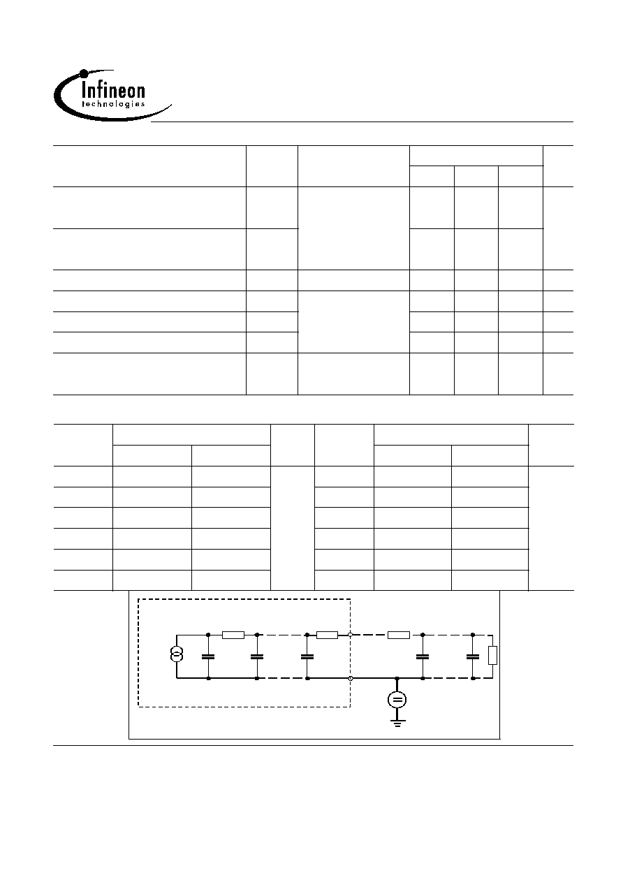
Typical Transient Thermal Characteristics
Symbol
Value
Unit
Symbol
Value
Unit
SPA
SPA
R
th1
0.00769
0.00769
K/W
C
th1
0.0003763
0.0003763
Ws/K
R
th2
0.015
0.015
C
th2
0.001411
0.001411
R
th3
0.029
0.029
C
th3
0.001931
0.001931
R
th4
0.114
0.163
C
th4
0.005297
0.005297
R
th5
0.136
0.323
C
th5
0.012
0.008453
R
th6
0.059
2.526
C
th6
0.091
0.412
SPP_B_I
SPP_B_I
External H eatsink
T
j
T
case
T
am b
C
th1
C
th2
R
th1
R
th,n
C
th,n
P
tot
(t)
2003-10-08
Page 5
SPP20N60C3, SPB20N60C3
SPI20N60C3, SPA20N60C3
Final data
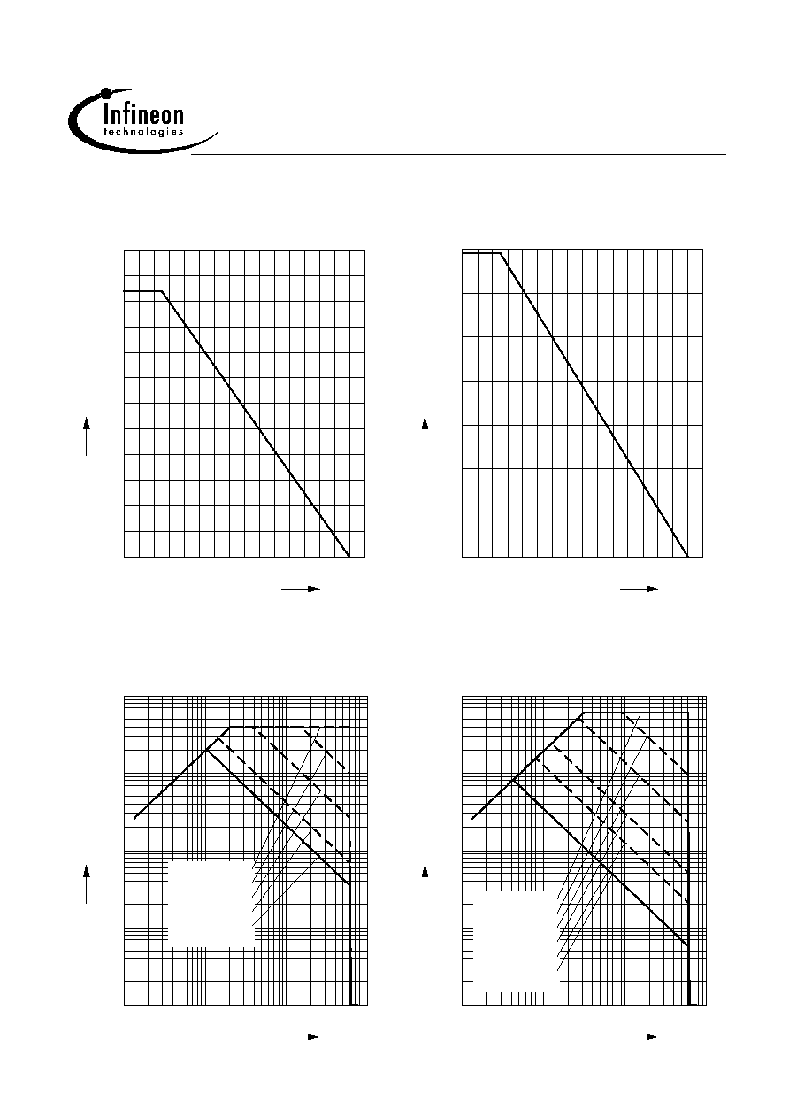
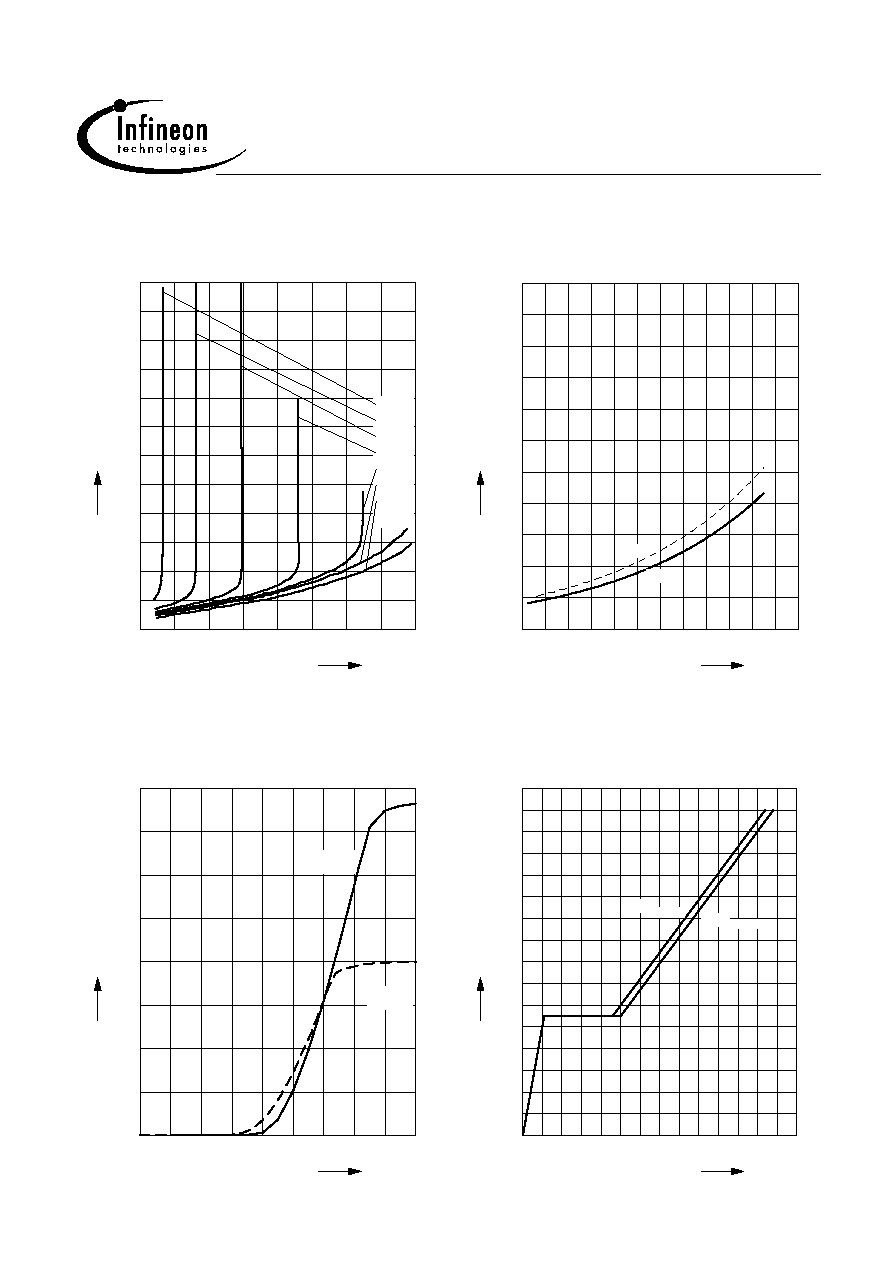
1 Power dissipation
P
tot
= f (
T
C
)
0
20
40
60
80
100
120
°C
160
T
C
0
20
40
60
80
100
120
140
160
180
200
W
240
SPP20N60C3
P
tot
2 Power dissipation FullPAK
P
tot
= f (
T
C
)
0
20
40
60
80
100
120
°C
160
T
C
0
5
10
15
20
25
W
35
P
tot
3 Safe operating area
I
D
= f ( V
DS
)
parameter : D = 0 ,
T
C
=25°C
10
0
10
1
10
2
10
3
V
V
DS
-2
10
-1
10
0
10
1
10
2
10
A
I
D
tp = 0.001 ms
tp = 0.01 ms
tp = 0.1 ms
tp = 1 ms
DC
4 Safe operating area FullPAK
I
D
= f (
V
DS
)
parameter: D = 0,
T
C
= 25°C
10
0
10
1
10
2
10
3
V
V
DS
-2
10
-1
10
0
10
1
10
2
10
A
I
D
tp = 0.001 ms
tp = 0.01 ms
tp = 0.1 ms
tp = 1 ms
tp = 10 ms
DC
2003-10-08
Page 6
SPP20N60C3, SPB20N60C3
SPI20N60C3, SPA20N60C3
Final data
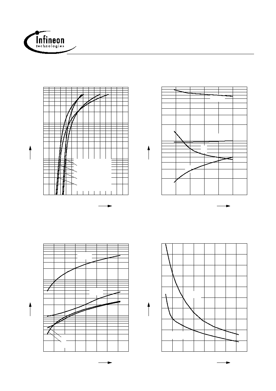
5 Transient thermal impedance
Z
thJC
= f (t
p
)
parameter: D = t
p
/T
10
-7
10
-6
10
-5
10
-4
10
-3
10
-2
10
0
s
t
p
-4
10
-3
10
-2
10
-1
10
0
10
K/W
Z
thJC
D = 0.5
D = 0.2
D = 0.1
D = 0.05
D = 0.02
D = 0.01
single pulse
6 Transient thermal impedance FullPAK
Z
thJC
= f (
t
p
)
parameter: D =
t
p
/t
10
-6
10
-5
10
-4
10
-3
10
-2
10
-1
10
1
s
t
p
-3
10
-2
10
-1
10
0
10
1
10
K/W
Z
thJC
D = 0.5
D = 0.2
D = 0.1
D = 0.05
D = 0.02
D = 0.01
single pulse
7 Typ. output characteristic
I
D
= f (
V
DS
);
T
j
=25°C
parameter: t
p
= 10 µs,
V
GS
0
5
10
15
V
25
V
DS
0
10
20
30
40
50
60
A
80
I
D
4,5V
5V
5,5V
6V
6,5V
7V
20V
10V
8V
8 Typ. output characteristic
I
D
= f (
V
DS
);
T
j
=150°C
parameter: t
p
= 10 µs,
V
GS
0
2
4
6
8 10 12 14 16 18 20 22
V
25
V
DS
0
5
10
15
20
25
30
35
A
45
I
D
4.5V
5V
5.5V
6V
20V
10V
7V
2003-10-08
Page 7
SPP20N60C3, SPB20N60C3
SPI20N60C3, SPA20N60C3
Final data
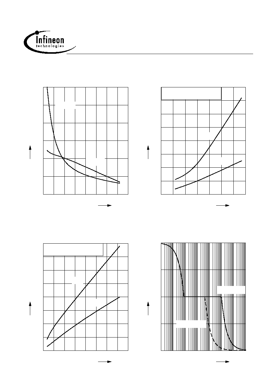
9 Typ. drain-source on resistance
R
DS(on)
=
f
(I
D
)
parameter:
T
j
=150°C,
V
GS
0
5
10
15
20
25
30
A
40
I
D
0.3
0.4
0.5
0.6
0.7
0.8
0.9
1
1.1
1.2
1.3
1.5
R
DS
(
on)
4V
4.5V
5V
5.5V
6V
6.5V
20V
10 Drain-source on-state resistance
R
DS(on)
= f (T
j
)
parameter : I
D
= 13.1 A,
V
GS
= 10 V
-60
-20
20
60
100
°C
180
T
j
0
0.1
0.2
0.3
0.4
0.5
0.6
0.7
0.8
0.9
1.1
SPP20N60C3
R
DS(on)
typ
98%
11 Typ. transfer characteristics
I
D
= f ( V
GS
); V
DS
2 x I
D
x R
DS(on)max
parameter: t
p
= 10 µs
0
1
2
3
4
5
6
7
V
9
V
GS
0
10
20
30
40
50
60
A
80
I
D
150°C
25°C
12 Typ. gate charge
V
GS
= f (Q
Gate
)
parameter: I
D
= 20.7 A pulsed
0
20
40
60
80
100
nC
140
Q
Gate
0
2
4
6
8
10
12
V
16
SPP20N60C3
V
GS
0,8 V
DS max
DS max
V
0,2
2003-10-08
Page 8
SPP20N60C3, SPB20N60C3
SPI20N60C3, SPA20N60C3
Final data
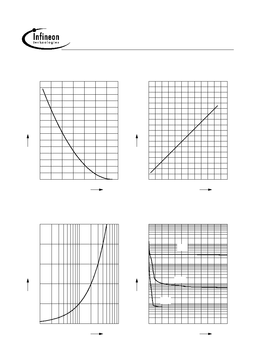
13 Forward characteristics of body diode
I
F
= f (V
SD
)
parameter: Tj , t
p
= 10 µs
0
0.4
0.8
1.2
1.6
2
2.4
V
3
V
SD
-1
10
0
10
1
10
2
10
A
SPP20N60C3
I
F
T
j
= 25 °C typ
T
j
= 25 °C (98%)
T
j
= 150 °C typ
T
j
= 150 °C (98%)
14 Typ. switching time
t = f (I
D
), inductive load,
T
j
=125°C
par.:
V
DS
=380V,
V
GS
=0/+13V,
R
G
=3.6
0
4
8
12
16
A
24
I
D
0
10
1
10
2
10
ns
t
tr
td(off)
td(on)
tf
15 Typ. switching time
t = f (
R
G
), inductive load,
T
j
=125°C
par.:
V
DS
=380V,
V
GS
=0/+13V, I
D
=20.7 A
0
5
10
15
20
25
30
40
R
G
0
10
1
10
2
10
3
10
ns
t
td(off)
td(on)
tr
tf
16 Typ. drain current slope
di/dt
= f(
R
G
), inductive load,
T
j
= 125°C
par.:
V
DS
=380V,
V
GS
=0/+13V, I
D
=20.7A
0
5
10
15
20
25
30
40
R
G
0
500
1000
1500
2000
2500
3000
3500
4000
A/µs
5000
d
i
/d
t
di/dt(on)
di/dt(off)
2003-10-08
Page 9
SPP20N60C3, SPB20N60C3
SPI20N60C3, SPA20N60C3
Final data
17 Typ. drain source voltage slope
dv/dt
= f(
R
G
), inductive load,
T
j
= 125°C
par.:
V
DS
=380V,
V
GS
=0/+13V, I
D
=20.7A
0
5
10
15
20
25
30
40
R
G
0
25
50
75
100
V/ns
150
d
v
/d
t
dv/dt(on)
dv/dt(off)
18 Typ. switching losses
E = f (I
D
), inductive load,
T
j
=125°C
par.:
V
DS
=380V,
V
GS
=0/+13V,
R
G
=3.6
0
3
6
9
12
15
A
21
I
D
0
0.01
0.02
0.03
0.04
0.05
0.06
mWs
0.08
E
Eon*
Eoff
*) Eon includes SPD06S60 diode
commutation losses
19 Typ. switching losses
E = f(
R
G
), inductive load,
T
j
=125°C
par.:
V
DS
=380V,
V
GS
=0/+13V, I
D
=20.7A
0
5
10
15
20
25
30
40
R
G
0
0.05
0.1
0.15
0.2
0.25
0.3
mWs
0.4
E
Eon*
Eoff
*) Eon includes SPD06S60 diode
commutation losses
20 Avalanche SOA
I
AR
= f (t
AR
)
par.:
T
j
150 °C
10
-3
10
-2
10
-1
10
0
10
1
10
2
10
4
µs
t
AR
0
5
10
A
20
I
AR
Tj(Start)=25°C
Tj(Start)=125°C
2003-10-08
Page 10
SPP20N60C3, SPB20N60C3
SPI20N60C3, SPA20N60C3
Final data
21 Avalanche energy
E
AS
= f (
T
j
)
par.: I
D
= 10 A,
V
DD
= 50 V
20
40
60
80
100
120
°C
160
T
j
0
50
100
150
200
250
300
350
400
450
500
550
600
mJ
750
E
AS
23 Avalanche power losses
P
AR
= f (
f
)
parameter:
E
AR
=1mJ
10
4
10
5
10
6
Hz
f
0
100
200
300
W
500
P
AR
22 Drain-source breakdown voltage
V
(BR)DSS
= f (
T
j
)
-60
-20
20
60
100
°C
180
T
j
540
560
580
600
620
640
660
680
V
720
SPP20N60C3
V
(BR)DSS
24 Typ. capacitances
C = f (
V
DS
)
parameter:
V
GS
=0V, f=1 MHz
0
100
200
300
400
V
600
V
DS
0
10
1
10
2
10
3
10
4
10
5
10
pF
C
Ciss
Coss
Crss
2003-10-08
Page 11
SPP20N60C3, SPB20N60C3
SPI20N60C3, SPA20N60C3
Final data
25 Typ.
C
oss
stored energy
E
oss
=
f
(
V
DS
)
0
100
200
300
400
V
600
V
DS
0
1
2
3
4
5
6
7
8
9
10
11
12
µJ
14
E
oss
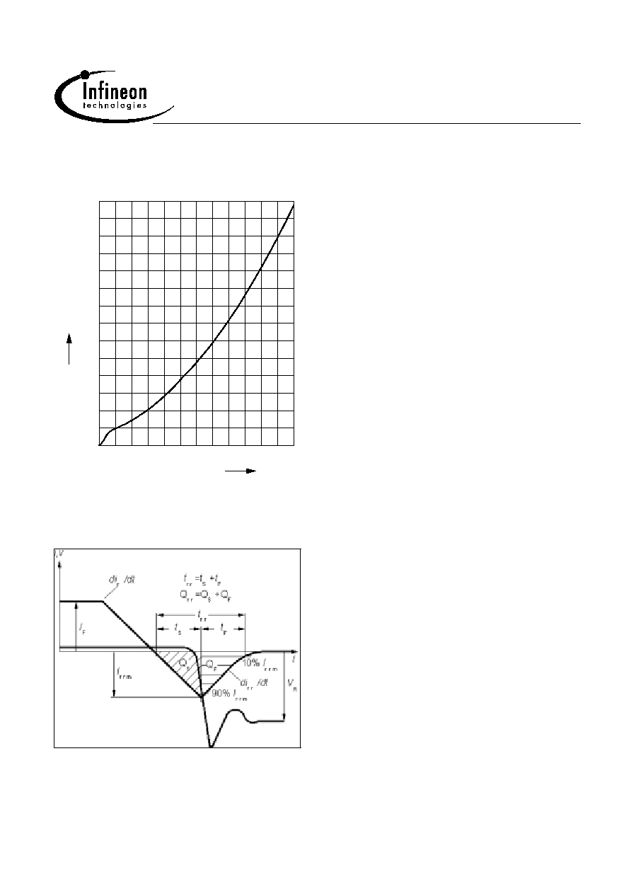
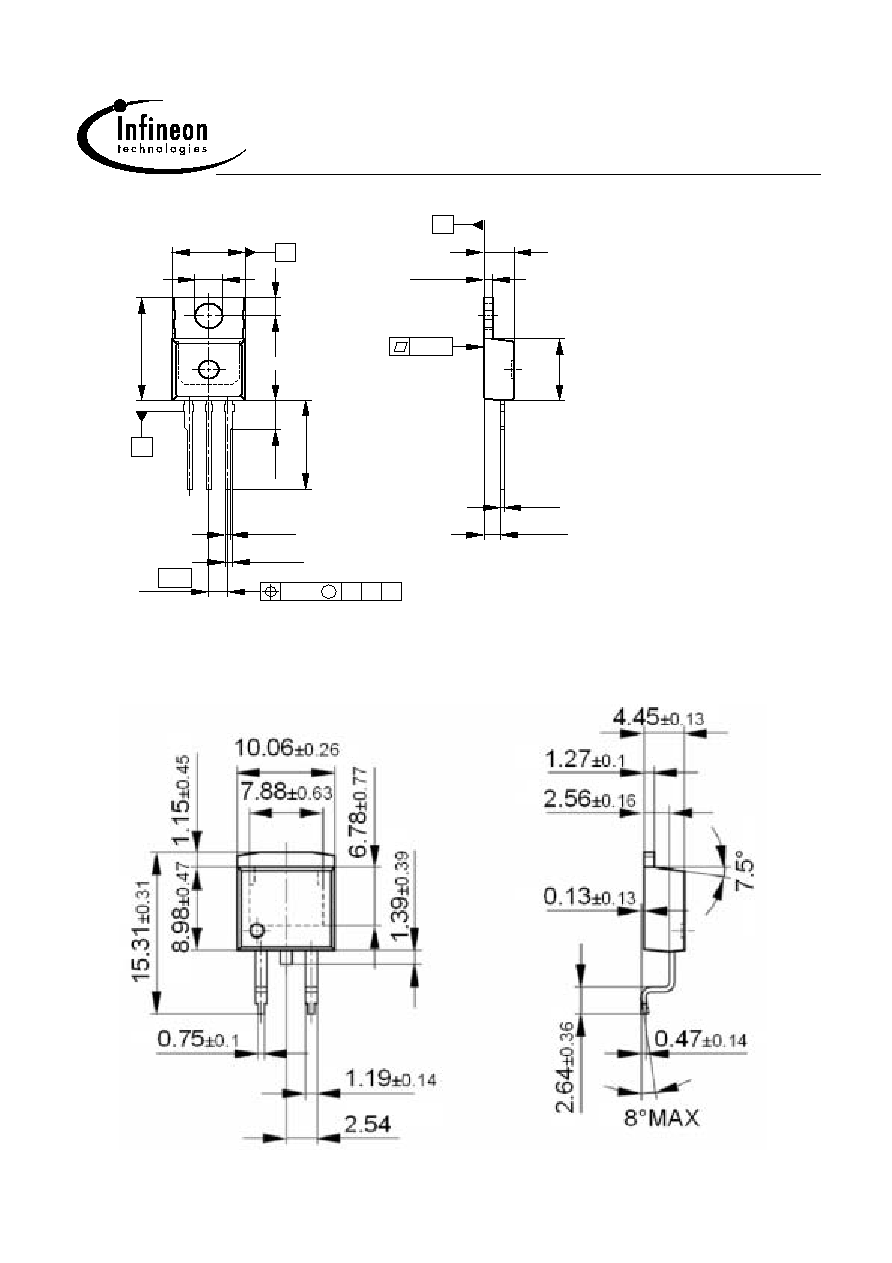
Definition of diodes switching characteristics
2003-10-08
Page 12
SPP20N60C3, SPB20N60C3
SPI20N60C3, SPA20N60C3
Final data
P-TO-220-3-1
A
B
A
0.25
M
2.8
15.38
±0.6
2.54
0.75
±0.1
±0.13
1.27
4.44
B
9.98
±0.48
0.05
All metal surfaces tin plated, except area of cut.
C
±0.2
10
±0.4
3.7
C
0.5
±0.1
±0.9
5.23
13.5
±0.5
3x
Metal surface min. x=7.25, y=12.3
2x
±0.2
±0.22
1.17
±0.2
2.51
P-TO-263-3-2 (D
2
-PAK)
2003-10-08
Page 13
SPP20N60C3, SPB20N60C3
SPI20N60C3, SPA20N60C3
Final data
P-TO-262-3-1 (I
2
-PAK)
B
A
0.25
M
Typical
2.54
3 x 0.75
±0.1
1.05
1.27
B
9.25
±0.2
0.05
1)
Metal surface min. X = 7.25, Y = 6.9
C
11.6
±0.3
10
±0.2
C
2.4
0.5
±0.1
±0.2
4.55
13.5
±0.5
All metal surfaces tin plated, except area of cut.
±0.3
1
8.5
1)
2 x
4.4
7.55
1)
0...0.15
0...0.3
2.4
A
P-TO-220-3-31 (FullPAK)
Please refer to mounting instructions (application note AN-TO220-3-31-01)

2003-10-08
Page 14
SPP20N60C3, SPB20N60C3
SPI20N60C3, SPA20N60C3
Final data
Published by
Infineon Technologies AG,
Bereichs Kommunikation
St.-Martin-Strasse 53,
D-81541 München
© Infineon Technologies AG 1999
All Rights Reserved.
Attention please!
The information herein is given to describe certain components and shall not be considered as warranted
characteristics.
Terms of delivery and rights to technical change reserved.
We hereby disclaim any and all warranties, including but not limited to warranties of non-infringement,
regarding circuits, descriptions and charts stated herein.
Infineon Technologies is an approved CECC manufacturer.
Information
For further information on technology, delivery terms and conditions and prices please contact your nearest
Infineon Technologies Office in Germany or our Infineon Technologies Reprensatives worldwide (see address list).
Warnings
Due to technical requirements components may contain dangerous substances.
For information on the types in question please contact your nearest Infineon Technologies Office.
Infineon Technologies Components may only be used in life-support devices or systems with the express
written approval of Infineon Technologies, if a failure of such components can reasonably be expected to
cause the failure of that life-support device or system, or to affect the safety or effectiveness of that device
or system Life support devices or systems are intended to be implanted in the human body, or to support
and/or maintain and sustain and/or protect human life. If they fail, it is reasonable to assume that the health
of the user or other persons may be endangered.