2004-03-01
Page 1
SPU01N60C3
SPD01N60C3
Rev. 2.0
Cool MOSTM
Power Transistor
V
DS
@ T
jmax
650
V
R
DS(on)
6
I
D
0.8
A
Feature
∑ New revolutionary high voltage technology
∑ Ultra low gate charge
∑ Periodic avalanche rated
∑ Extreme dv/dt rated
∑ Ultra low effective capacitances
∑ Improved transconductance
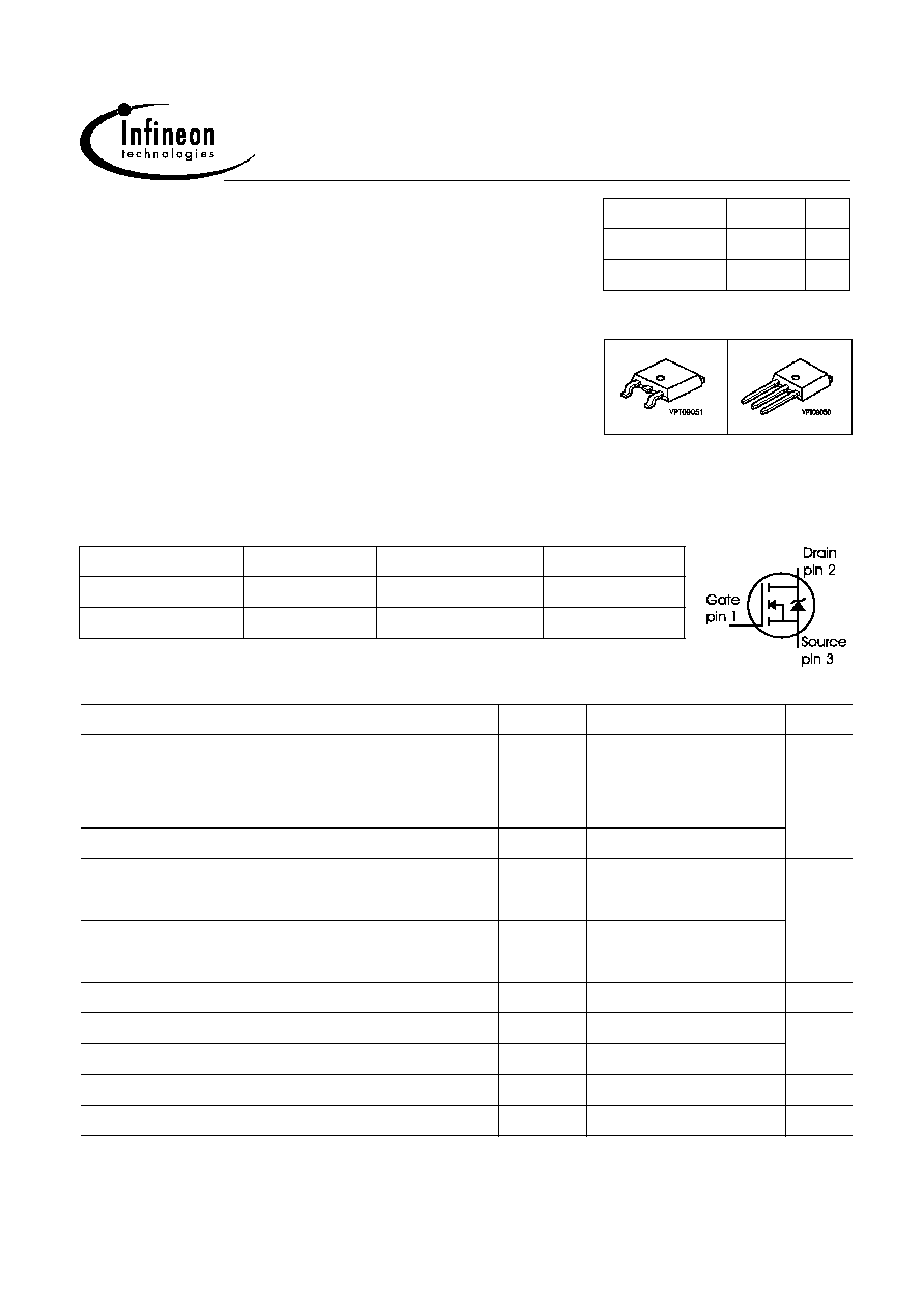
P-TO251-3-1
P-TO252
Type
Package
Ordering Code
SPU01N60C3
P-TO251-3-1
Q67040-S4193
SPD01N60C3
P-TO252
Q67040-S4188
Marking
01N60C3
01N60C3
Maximum Ratings
Parameter
Symbol
Value
Unit
Continuous drain current
T
C
= 25 ∞C
T
C
= 100 ∞C
I
D
0.8
0.5
A
Pulsed drain current, t
p
limited by T
jmax
I
D puls
1.6
Avalanche energy, single pulse
I
D
= 0.6 A, V
DD
= 50 V
E
AS
20
mJ
Avalanche energy, repetitive t
AR
limited by T
jmax
1)
I
D
= 0.8 A, V
DD
= 50 V
E
AR
0.01
Avalanche current, repetitive t
AR
limited by T
jmax
I
AR
0.8
A
Gate source voltage static
V
GS
±20
V
Gate source voltage AC (f >1Hz)
V
GS
±30
Power dissipation,
T
C
= 25∞C
P
tot
11
W
Operating and storage temperature
T
j ,
T
stg
-55... +150
∞C

2004-03-01
Page 2
SPU01N60C3
SPD01N60C3
Rev. 2.0
Maximum Ratings
Parameter
Symbol
Value
Unit
Drain Source voltage slope
V
DS
= 480 V, I
D
= 0.8 A, T
j
= 125 ∞C
dv/dt
50
V/ns
Thermal Characteristics
Parameter
Symbol
Values
Unit
min.
typ.
max.
Thermal resistance, junction - case
R
thJC
-
-
11
K/W
Thermal resistance, junction - ambient, leaded
R
thJA
-
-
75
SMD version, device on PCB:
@ min. footprint
@ 6 cm
2
cooling area
2)
R
thJA
-
-
-
-
75
50
Soldering temperature,
1.6 mm (0.063 in.) from case for 10s
T
sold
-
-
260
∞C
Electrical Characteristics, at Tj=25∞C unless otherwise specified
Parameter
Symbol
Conditions
Values
Unit
min.
typ.
max.
Drain-source breakdown voltage V
(BR)DSS V
GS
=0V, I
D
=0.25mA
600
-
-
V
Drain-Source avalanche
breakdown voltage
V
(BR)DS
V
GS
=0V, I
D
=0.8A
-
700
-
Gate threshold voltage
V
GS(th)
I
D
=250
µ, V
GS
=V
DS
2.1
3
3.9
Zero gate voltage drain current
I
DSS
V
DS
=600V, V
GS
=0V,
T
j
=25∞C,
T
j
=150∞C
-
-
0.1
-
1
50
µA
Gate-source leakage current
I
GSS
V
GS
=30V, V
DS
=0V
-
-
100
nA
Drain-source on-state resistance R
DS(on)
V
GS
=10V, I
D
=0.5A,
T
j
=25∞C
T
j
=150∞C
-
-
5.6
15.1
6
-

2004-03-01
Page 3
SPU01N60C3
SPD01N60C3
Rev. 2.0
Electrical Characteristics , at T
j
= 25 ∞C, unless otherwise specified
Parameter
Symbol
Conditions
Values
Unit
min.
typ.
max.
Transconductance
g
fs
V
DS
2*I
D
*R
DS(on)max
,
I
D
=0.5A
-
0.75
-
S
Input capacitance
C
iss
V
GS
=0V, V
DS
=25V,
f
=1MHz
-
100
-
pF
Output capacitance
C
oss
-
40
-
Reverse transfer capacitance
C
rss
-
2.5
-
Turn-on delay time
t
d(on)
V
DD
=350V, V
GS
=0/10V,
I
D
=0.8A, R
G
=100
-
30
-
ns
Rise time
t
r
-
25
-
Turn-off delay time
t
d(off)
-
55
82
Fall time
t
f
-
30
45
Gate Charge Characteristics
Gate to source charge
Q
gs
V
DD
=350V, I
D
=0.8A
-
0.9
-
nC
Gate to drain charge
Q
gd
-
2.2
-
Gate charge total
Q
g
V
DD
=350V, I
D
=0.8A,
V
GS
=0 to 10V
-
3.9
5
Gate plateau voltage
V
(plateau)
V
DD
=350V, I
D
=0.8A
-
5.5
-
V
1Repetitve avalanche causes additional power losses that can be calculated as P
AV
=E
AR
*f.
2Device on 40mm*40mm*1.5mm epoxy PCB FR4 with 6cm≤ (one layer, 70 µm thick) copper area for drain
connection. PCB is vertical without blown air.
2004-03-01
Page 4
SPU01N60C3
SPD01N60C3
Rev. 2.0
Electrical Characteristics, at T
j
= 25 ∞C, unless otherwise specified
Parameter
Symbol
Conditions
Values
Unit
min.
typ.
max.
Inverse diode continuous
forward current
I
S
T
C
=25∞C
-
-
0.8
A
Inverse diode direct current,
pulsed
I
SM
-
-
1.6
Inverse diode forward voltage
V
SD
V
GS
=0V, I
F
=I
S
-
1
1.2
V
Reverse recovery time
t
rr
V
R
=350V, I
F
=I
S
,
di
F
/dt
=100A/µs
-
570
970
ns
Reverse recovery charge
Q
rr
-
0.75
-
µC
Typical Transient Thermal Characteristics
Symbol
Value
Unit
Symbol
Value
Unit
typ.
typ.
Thermal resistance
R
th1
0.225
K/W
R
th2
0.395
R
th3
0.603
R
th4
0.995
R
th5
0.691
R
th6
0.148
Thermal capacitance
C
th1
0.00001221
Ws/K
C
th2
0.00005037
C
th3
0.0000809
C
th4
0.0002915
C
th5
0.001844
C
th6
0.412
External H eatsink
T
j
T
case
T
am b
C
th1
C
th2
R
th1
R
th,n
C
th,n
P
tot
(t)
2004-03-01
Page 5
SPU01N60C3
SPD01N60C3
Rev. 2.0
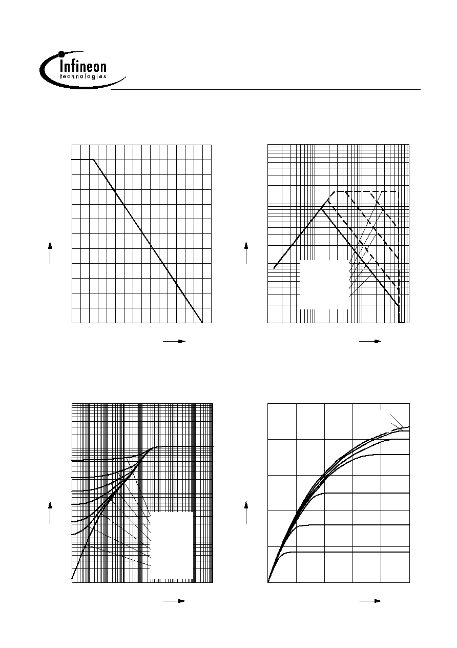
1 Power dissipation
P
tot
= f (T
C
)
0
20
40
60
80
100
120
∞C
160
T
C
0
1
2
3
4
5
6
7
8
9
10
W
12
SPU01N60C3
P
tot
2 Safe operating area
I
D
= f ( V
DS
)
parameter : D = 0 , T
C
=25∞C
10
0
10
1
10
2
10
3
V
V
DS
-2
10
-1
10
0
10
1
10
A
I
D
tp = 0.001 ms
tp = 0.01 ms
tp = 0.1 ms
tp = 1 ms
DC
3 Transient thermal impedance
Z
thJC
= f (t
p
)
parameter: D = t
p
/T
10
-7
10
-6
10
-5
10
-4
10
-3
10
-2
10
-1
10
1
s
t
p
-2
10
-1
10
0
10
1
10
2
10
K/W
Z
thJC
D = 0.5
D = 0.2
D = 0.1
D = 0.05
D = 0.02
D = 0.01
single pulse
4 Typ. output characteristic
I
D
= f (V
DS
); T
j
=25∞C
parameter: t
p
= 10 µs, V
GS
0
5
10
15
V
25
V
DS
0
0.5
1
1.5
A
2.5
I
D
5V
5.5V
6V
6.5V
7V
20V
10V