
LXT970A
Dual-Speed Fast Ethernet Transceiver
Datasheet
The LXT970A is an enhanced derivative of the LXT970 10/100 Mbps Fast Ethernet PHY
Transceiver that supports selectable driver strength capabilities and link-loss criteria. The
LXT970A supports 100BASE-TX, 10BASE-T, and 100BASE-FX applications. It provides a
Media Independent Interface (MII) for easy attachment to 10/100 Media Access Controllers
(MAC)s and a pseudo-ECL interface for use with 100BASE-FX fiber networks.
The LXT970A supports full-duplex operation at 10 and 100 Mbps. Its operating condition is set
using auto-negotiation, parallel detection or manual control. The encoder may be bypassed for
symbol mode applications.
The LXT970A is fabricated with an advanced CMOS process and requires only a single 5V
power supply. The MII may be operated independently with either a 5V or a 3.3V supply.
Applications
Product Features
s
Combination 10BASE-T/100BASE-TX
Network Interface Cards (NICs)
s
10/100 Switches, 10/100 Printservers
s
100BASE-FX Network Interface Cards
(NICs)
s
IEEE 802.3 Compliant:
-- 10BASE-T and 100BASE-TX using a
single RJ-45 connection.
-- Supports auto-negotiation and parallel
detection for legacy systems.
-- MII interface with extended register
capability.
s
Robust baseline wander correction
performance.
s
100BASE-FX fiber optic capable.
s
Standard CSMA/CD or full-duplex
operation.
s
Configurable via MII serial port or external
control pins.
s
Configurable for DTE or switch
applications.
s
CMOS process with single 5Vsupply
operation
with provision for interface to 3.3V MII
bus.
s
Integrated LED drivers.
s
Integrated supply monitor and line
disconnect during low supply fault.
s
Available in:
-- 64-pin TQFP (LXT970ATC)
-- 64-pin PQFP (LXT970AQC)
s
Commercial temperature range (0 - 70
o
C
ambient).
As of January 15, 2001, this document replaces the Level One document
Order Number: 249099-001
LXT970A -- Dual-Speed Fast Ethernet Transceiver.
January 2001

Datasheet
Information in this document is provided in connection with Intel
�
products. No license, express or implied, by estoppel or otherwise, to any intellectual
property rights is granted by this document. Except as provided in Intel's Terms and Conditions of Sale for such products, Intel assumes no liability
whatsoever, and Intel disclaims any express or implied warranty, relating to sale and/or use of Intel products including liability or warranties relating to
fitness for a particular purpose, merchantability, or infringement of any patent, copyright or other intellectual property right. Intel products are not
intended for use in medical, life saving, or life sustaining applications.
Intel may make changes to specifications and product descriptions at any time, without notice.
Designers must not rely on the absence or characteristics of any features or instructions marked "reserved" or "undefined." Intel reserves these for
future definition and shall have no responsibility whatsoever for conflicts or incompatibilities arising from future changes to them.
The LXT970A may contain design defects or errors known as errata which may cause the product to deviate from published specifications. Current
characterized errata are available on request.
Contact your local Intel sales office or your distributor to obtain the latest specifications and before placing your product order.
Copies of documents which have an ordering number and are referenced in this document, or other Intel literature may be obtained by calling 1-800-
548-4725 or by visiting Intel's website at http://www.intel.com.
Copyright � Intel Corporation, 2001
*Third-party brands and names are the property of their respective owners.

Datasheet
3
Dual-Speed Fast Ethernet Transceiver -- LXT970A
Contents
1.0
Pin Assignments and Signal Descriptions
.................................................... 10
2.0
Functional Description
........................................................................................... 18
2.1
Introduction.......................................................................................................... 18
2.2
Interfaces (Network Media/Protocol Support) ..................................................... 19
2.2.1
Twisted-Pair Interface ............................................................................19
2.2.2
Fiber Interface ........................................................................................ 19
2.2.3
MII Interface ........................................................................................... 20
2.2.3.1 Selectable Driver Levels............................................................ 20
2.2.3.2 MII Data Interface ...................................................................... 21
2.2.3.3 Repeater Mode.......................................................................... 24
2.2.3.4 MII Management Interface ........................................................ 24
2.2.4
Hardware Control Interface .................................................................... 26
2.3
Operating Requirements ..................................................................................... 27
2.3.1
Power Supply Requirements.................................................................. 27
2.3.1.1 Optional MII Power Supply ........................................................ 27
2.3.2
Reference Clock Requirements ............................................................. 27
2.3.2.1 Master Clock Mode ................................................................... 28
2.3.2.2 Slave Clock Mode .....................................................................28
2.3.3
Bias Circuit Requirements...................................................................... 29
2.4
Initialization.......................................................................................................... 29
2.4.1
Control Mode Selection .......................................................................... 29
2.4.1.1 MDIO Control Mode .................................................................. 29
2.4.1.2 Manual Control Mode ................................................................ 29
2.4.2
Link Configuration ..................................................................................29
2.4.2.1 Manual Configuration ................................................................ 30
2.4.2.2 Auto-Negotiation/Parallel Detection .......................................... 30
2.5
Monitoring Operational Status............................................................................. 31
2.5.1
Monitoring Status via MII Registers........................................................ 31
2.5.2
Monitoring Status via Indicator Pins ....................................................... 32
2.6
100BASE-X Operation ........................................................................................ 32
2.6.1
100BASE-X MII Operations.................................................................... 32
2.6.2
100BASE-X Network Operations ........................................................... 33
2.7
10BASE-T Operation........................................................................................... 35
2.7.1
10BASE-T MII Operations...................................................................... 35
2.7.2
10BASE-T Network Operations.............................................................. 35
2.8
Protocol Sublayer Operations ............................................................................. 35
2.8.1
PCS Sublayer .........................................................................................35
2.8.1.1 100X Preamble Handling .......................................................... 36
2.8.1.2 10T Preamble Handling............................................................. 36
2.8.1.3 Data Errors (100X Only) ............................................................ 36
2.8.1.4 Collision Indication .................................................................... 37
2.8.1.5 SQE (10T Only) ......................................................................... 38
2.8.1.6 Jabber (10T Only) .....................................................................38
2.8.2
PMA Layer.............................................................................................. 38
2.8.2.1 100TX Link Options ................................................................... 38
2.8.2.2 10T Link Test............................................................................. 38

LXT970A -- Dual-Speed Fast Ethernet Transceiver
4
Datasheet
2.8.2.3 Carrier Sense (CRS) ................................................................. 38
2.8.3
Twisted-Pair PMD Layer ........................................................................ 39
2.8.3.1 Scrambler/Descrambler (100TX Only) ...................................... 39
2.8.3.2 Baseline Wander Correction
(100TX Only)39
2.8.3.3 Polarity Correction..................................................................... 39
2.8.4
Fiber PMD Layer .................................................................................... 39
2.8.5
Additional Operating Features ............................................................... 40
2.8.6
Low-Voltage-Fault Detect....................................................................... 40
2.8.7
Power Down Mode ................................................................................. 40
2.8.8
Software Reset....................................................................................... 40
2.8.9
Hardware Reset ..................................................................................... 40
3.0
Application Information
......................................................................................... 41
3.1
Magnetics Information ......................................................................................... 41
3.2
Crystal Information .............................................................................................. 41
3.3
Design Recommendations .................................................................................. 42
3.3.1
General Design Guidelines .................................................................... 42
3.3.2
Power Supply Filtering ........................................................................... 42
3.3.3
Ground Noise ......................................................................................... 43
3.3.4
Power and Ground Plane Layout Considerations .................................. 43
3.3.5
Interfaces for Twisted-Pair /Fiber ........................................................... 43
3.3.5.1 Twisted-Pair .............................................................................. 43
3.3.5.2 Fiber .......................................................................................... 44
3.3.6
Interface for the MII ................................................................................ 44
3.3.6.1 Transmit Hold Time Adjustment ................................................ 44
3.3.6.2 MII Terminations........................................................................ 44
3.3.7
Typical Application ................................................................................. 45
3.3.7.1 Voltage Divider For MF Inputs................................................... 45
4.0
Test Specifications
.................................................................................................. 47
5.0
Register Definitions
................................................................................................ 63
6.0
Mechanical Specifications
................................................................................... 73

Datasheet
5
Dual-Speed Fast Ethernet Transceiver -- LXT970A
Figures
1
LXT970A Block Diagram ....................................................................................... 9
2
LXT970A Pin Assignments ................................................................................. 10
3
Network Interface Card (NIC) Application .......................................................... 18
4
MII Interface ....................................................................................................... 20
5
MII Data Interface ...............................................................................................21
6
Loopback Paths .................................................................................................. 23
7
Repeater Block Diagram .................................................................................... 24
8
MDIO Interrupt Signaling .................................................................................... 25
9
Management Interface - Read Frame Structure ................................................. 25
10
Management Interface - Write Frame Structure ................................................. 25
11
LXT970A Initialization Sequence ....................................................................... 30
12
Auto-Negotiation Operation ................................................................................ 31
13
100BASE-TX Frame Structure ........................................................................... 33
14
100BASE-TX Data Flow ..................................................................................... 33
15
LXT970A Protocol Sublayers ............................................................................. 36
16
100BASE-TX Reception with No Errors ............................................................. 37
17
100BASE-TX Reception with Invalid Symbol .................................................... 37
18
100BASE-TX Transmission with No Errors ....................................................... 37
19
100BASE-TX Transmission with Collision ......................................................... 37
20
Voltage Divider ................................................................................................... 45
21
Typical Interface Circuitry ................................................................................... 46
22
MII - 100BASE-TX Receive Timing / 4B Mode ................................................... 51
23
MII - 100BASE-TX Transmit Timing / 4B Mode ................................................. 52
24
MII - 100BASE-TX Receive Timing / 5B Mode ................................................... 53
25
100BASE-TX Transmit Timing / 5B Mode .......................................................... 54
26
MII - 100BASE-FX Receive Timing / 4B Mode ................................................... 55
27
MII - 100BASE-FX Transmit Timing / 4B Mode ..................................................56
28
MII - 10BASE-T Receiving Timing ...................................................................... 57
29
MII - 10BASE-T Transmit Timing ....................................................................... 58
30
10BASE-T SQE (Heartbeat) Timing ................................................................... 59
31
10BASE-T Jab and Unjab Timing ...................................................................... 59
32
Auto Negotiation and Fast Link Pulse Timing .................................................... 60
33
Fast Link Pulse Timing ....................................................................................... 60
34
MDIO Timing when Sourced by STA ................................................................. 61
35
MDIO Timing when Sourced by PHY ................................................................. 61
36
Power-Down Recovery Timing (Over Recommended Range) ........................... 62
37
PHY Identifier Bit Mapping ................................................................................. 66
38
64-Pin QFP Package Diagram ........................................................................... 73
39
64-Pin TQFP Package Diagram ......................................................................... 74

LXT970A -- Dual-Speed Fast Ethernet Transceiver
6
Datasheet
Tables
1
LXT970A Power Supply Signal Descriptions ...................................................... 10
2
LXT970A MII Signal Descriptions ....................................................................... 11
3
LXT970A Fiber Interface Signal Descriptions ..................................................... 12
4
LXT970A Twisted-Pair Interface Signal Descriptions ......................................... 13
5
LXT970A LED Indicator Signal Descriptions....................................................... 13
6
LXT970A Miscellaneous Signal Descriptions...................................................... 13
7
LXT970A Hardware Control Interface Signal Descriptions ................................. 14
8
MF Pin Function Settings1, 3 .............................................................................. 16
9
LXT970A Auto-Negotiation Operating Speed/Full-Duplex
Advertisement Settings ....................................................................................... 17
10
Test Loopback Operation .................................................................................... 23
11
Carrier Sense, Loopback, and Collision Conditions............................................ 23
12
Configuring the LXT970A via Hardware Control ................................................. 26
13
LXT970A Operating Configurations / Auto-Negotiation Enabled ........................ 26
14
LXT970A Operating Configurations / Auto-Negotiation Disabled ....................... 27
15
Mode Control Settings......................................................................................... 29
16
LXT970A Status using FDS/LED Pins ................................................................ 32
17
4B/5B Coding ...................................................................................................... 34
18
Magnetics Requirements .................................................................................... 41
19
Crystal Requirements.......................................................................................... 41
20
Crystal Component Manufacturers ..................................................................... 41
21
Absolute Maximum Ratings ................................................................................ 47
22
Operating Conditions .......................................................................................... 47
23
Digital I/O Characteristics1.................................................................................. 48
24
Digital I/O Characteristics - MultiFunction Pins MF<4:0>.................................... 48
25
Required Clock Characteristics........................................................................... 48
26
Low Voltage Fault Detect Characteristics ........................................................... 49
27
100BASE-TX Transceiver Characteristics .......................................................... 49
28
100BASE-FX Transceiver Characteristics .......................................................... 49
29
10BASE-T Transceiver Characteristics............................................................... 50
30
10BASE-T Link Integrity Timing Characteristics ................................................. 50
31
MII - 100BASE-TX Receive Timing Parameters / 4B Mode ................................ 51
32
MII - 100BASE-TX Transmit Timing Parameters / 4B Mode ............................... 52
33
MII - 100BASE-TX Receive Timing Parameters / 5B Mode ................................ 53
34
MII - 100BASE-TX Transmit Timing Parameters / 5B Mode ............................... 54
35
MII - 100BASE-FX Receive Timing Parameters / 4B Mode ................................ 55
36
MII - 100BASE-FX Transmit Timing Parameters / 4B Mode ............................... 56
37
MII - 10BASE-T Receive Timing Parameters...................................................... 57
38
MII - 10BASE-T Transmit Timing Parameters..................................................... 58
39
10BASE-T SQE (Heartbeat) Timing Parameters ................................................ 59
40
10BASE-T Jab and Unjab Timing Parameters.................................................... 59
41
Auto Negotiation and Fast Link Pulse Timing Parameters.................................. 60
42
MDIO Timing Parameters ................................................................................... 61
43
Power-Down Recovery Timing Parameters ........................................................ 62
44
Register Set ........................................................................................................ 63
45
Control Register (Address 0)............................................................................... 64
46
Status Register (Address 1) ................................................................................ 65
47
PHY Identification Register 1 (Address 2)........................................................... 66
48
PHY Identification Register 2 (Address 3)........................................................... 66

Datasheet
7
Dual-Speed Fast Ethernet Transceiver -- LXT970A
49
Auto Negotiation Advertisement Register (Address 4)........................................ 67
50
Auto Negotiation Link Partner Ability Register (Address 5)................................. 68
51
Auto Negotiation Expansion (Address 6) ............................................................ 69
52
Mirror Register (Address 16, Hex 10).................................................................. 69
53
Interrupt Enable Register (Address 17, Hex 11) ................................................. 70
54
Interrupt Status Register (Address 18, Hex 12) ..................................................70
55
Configuration Register (Address 19, Hex 13)...................................................... 71
56
Chip Status Register (Address 20, Hex 14) ........................................................ 72
LXT970A -- Dual-Speed Fast Ethernet Transceiver
8
Datasheet
Revision History
Revision
Date
Description
Dual-Speed Fast Ethernet Transceiver -- LXT970A
Datasheet
9
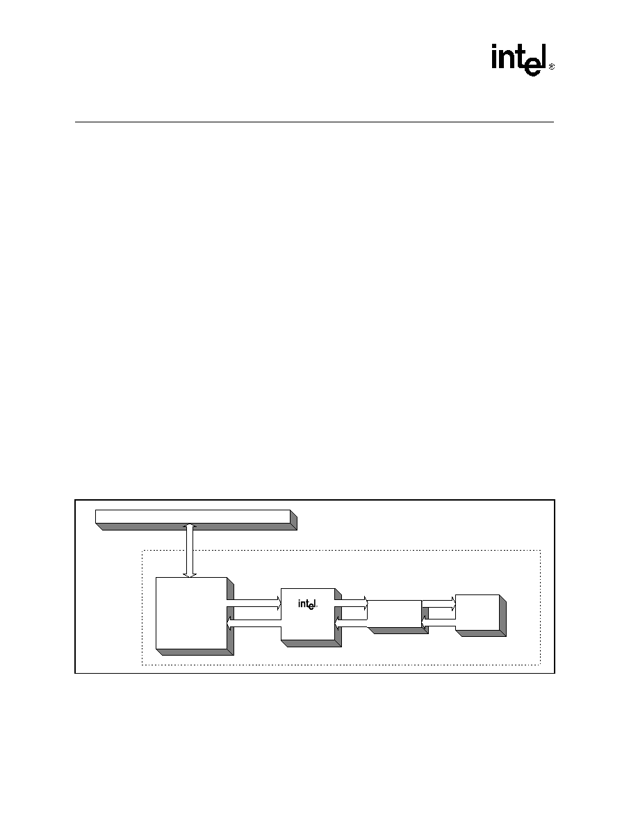
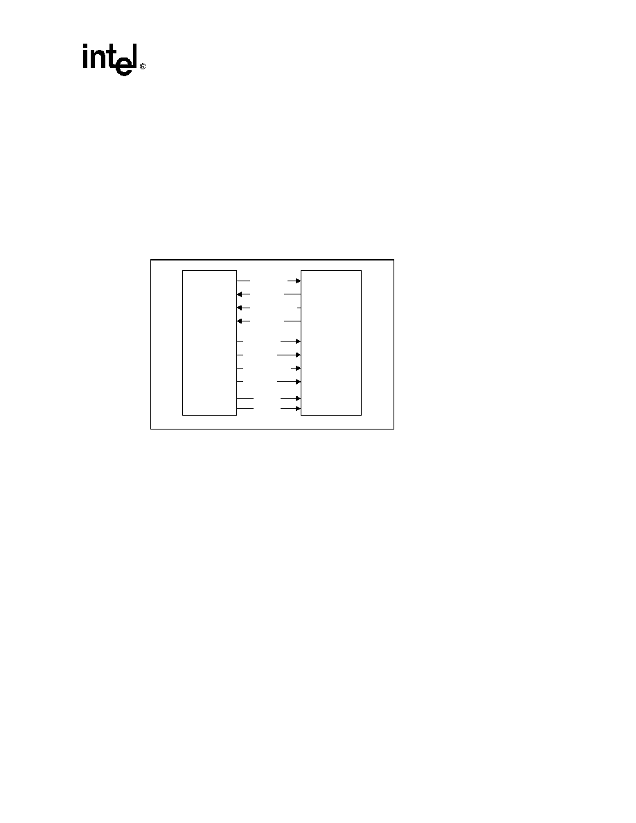
Figure 1. LXT970A Block Diagram
Management/
Mode Select
Logic
Decoder &
Descrambler
RXD<0:4>
FIBON
FIBOP
+
-
ECL
Driver
TPON
TPOP
+
TP
Driver
FIBIN
FIBIP
+
-
ECL
Rcvr
TPIN
TPIP
+
-
TP
Rcvr
Serial to
Parallel
Converter
Scrambler
& Encoder
TX_CLK
TXD<0:4>
Parallel
to Serial
Converter
TX_ER
TX_EN
Carrier Sense
Collision Detect
Data Valid
Error Detect
COL
CRS
RX_ER
RX_DV
MF<0:4>
CFG<0:1>
Crystal Osc
& PLL
RX_CLK
LED
Drivers
TRSTE
LED_
RESET
FDS/MDINT
MDIO
XTALI/O
Clock
Generator
Auto
Negotiation
Baseline
Wander
Correction
MDDIS
PwrDown/
Line Energy
Monitor
PWR_DWN
FDE
Slicer
Manchester
Decoder
Pulse
Shaper
Manchester
Encoder
10
100
10
100
MII
TX
MII
RX
MII
MGMT
2
-
100Mbps
Loopback
10Mbps
Loopback
MDC
Hardware
Interface
LXT970A -- Dual-Speed Fast Ethernet Transceiver
10
Datasheet
1.0
Pin Assignments and Signal Descriptions
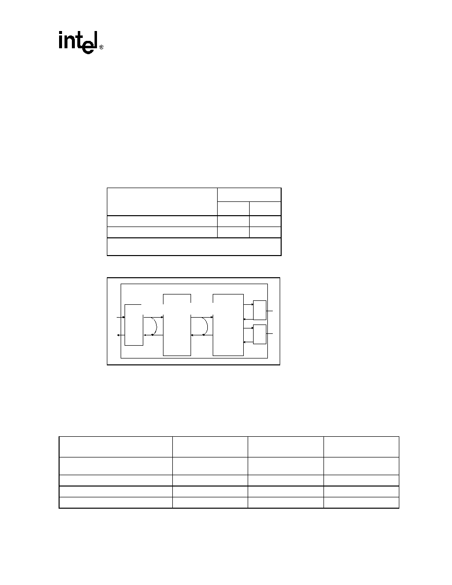
Figure 2. LXT970A Pin Assignments
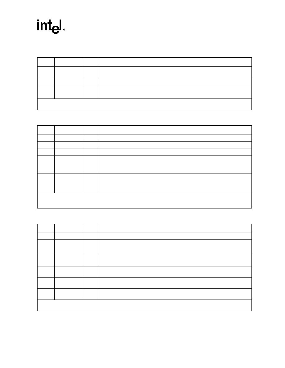
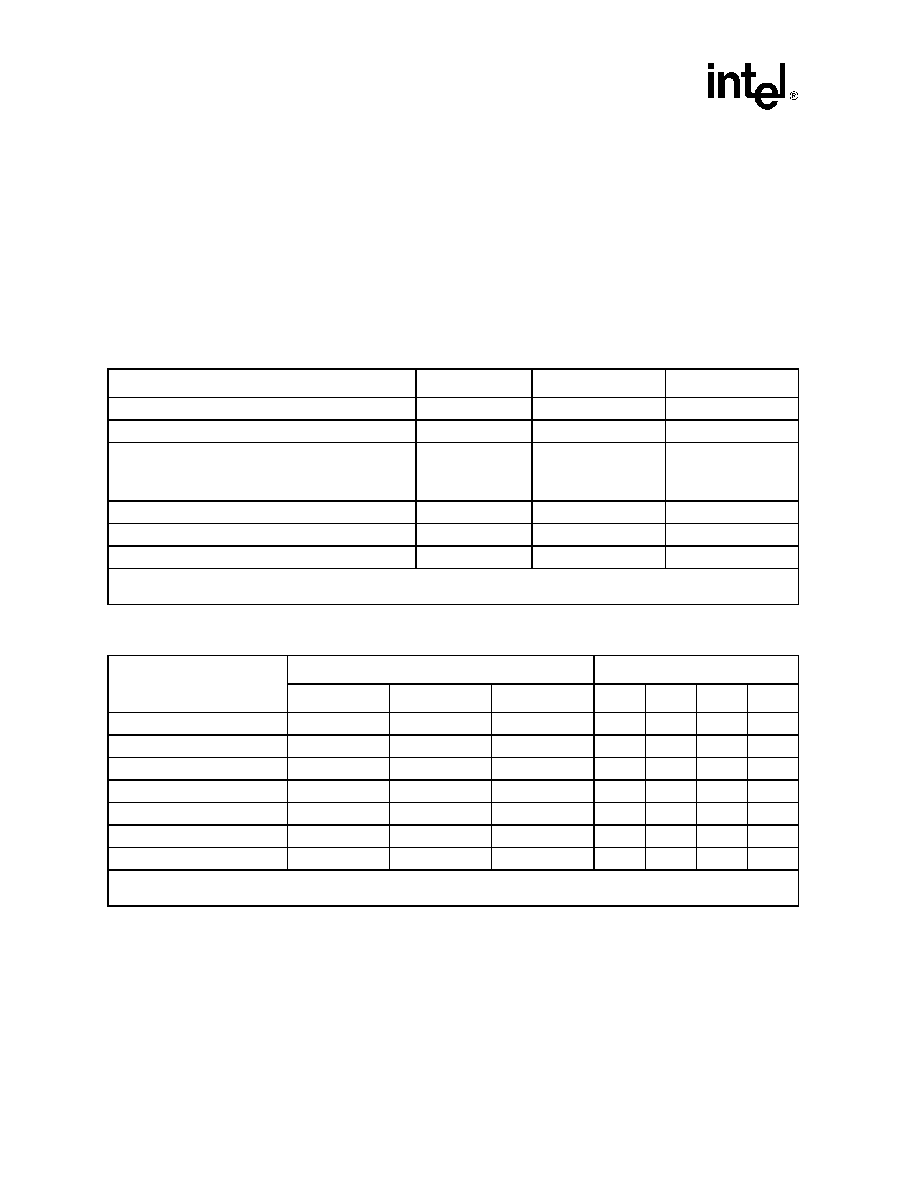
Table 1. LXT970A Power Supply Signal Descriptions
Pin#
1
Pin Name
I/O
Signal Description
19, 22
VCCT, GNDT
-
Transmitter Supply (+5V) and Ground. (Analog plane)
37, 31
VCCR, NDR
-
Receiver Supply (+5V) and Ground. (Analog plane)
24, 26
VCCA, NDA
-
Analog Supply (+5V) and Ground.
9, 43
VCCD, GNDD
-
Digital Supply (+5V) and Ground.
53, 52
VCCIO, GNDIO
-
MII Supply (+3.3V or +5V) and Ground. (Digital plane)
1. Pin numbers apply to all package types.
1
2
3
4
5
6
7
8
9
10
11
12
13
14
15
16
48
47
46
45
44
43
42
41
40
39
38
37
36
35
34
33
17
18
19
20
21
22
23
24
25
26
27
28
29
30
31
32
64
63
62
61
60
59
58
57
56
55
54
53
52
51
50
49
RXD2
RXD3
RXD4
MDC
MDIO
GNDD
LEDR
LEDT
LEDL
LEDC
LEDS
VCCR
N/C
N/C
PWRDWN
CFG1
CRS
FDS/MDINT
TRSTE
MF4
MF3
MF2
MF1
MF0
VCCD
TEST
XO
XI
FDE
CFG0
MDDIS
RESET
COL
TXD4
TXD3
TXD2
TXD1
TXD0
TX_
E
N
TX_
C
L
K
TX_
E
R
RX
_E
R
RX
_CL
K
V
CCIO
GNDI
O
RX
_DV
RX
D0
RX
D1
FIBOP
FI
BO
N
V
CCT
TRE
F
TPOP
GNDT
TP
ON
VC
C
A
RB
IA
S
GN
D
A
FIB
I
P
FIBIN
TP
I
P
TPIN
GNDR
N/C
LXT970AQC/ATC XX
XXXXXX
XXXXXXXX
Part #
LOT #
FPO #
Rev #

Dual-Speed Fast Ethernet Transceiver -- LXT970A
Datasheet
11
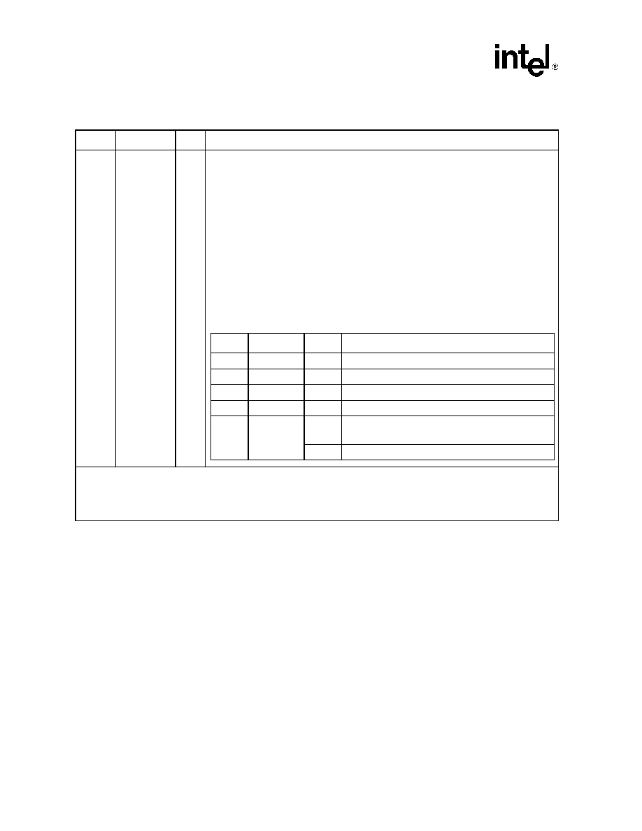
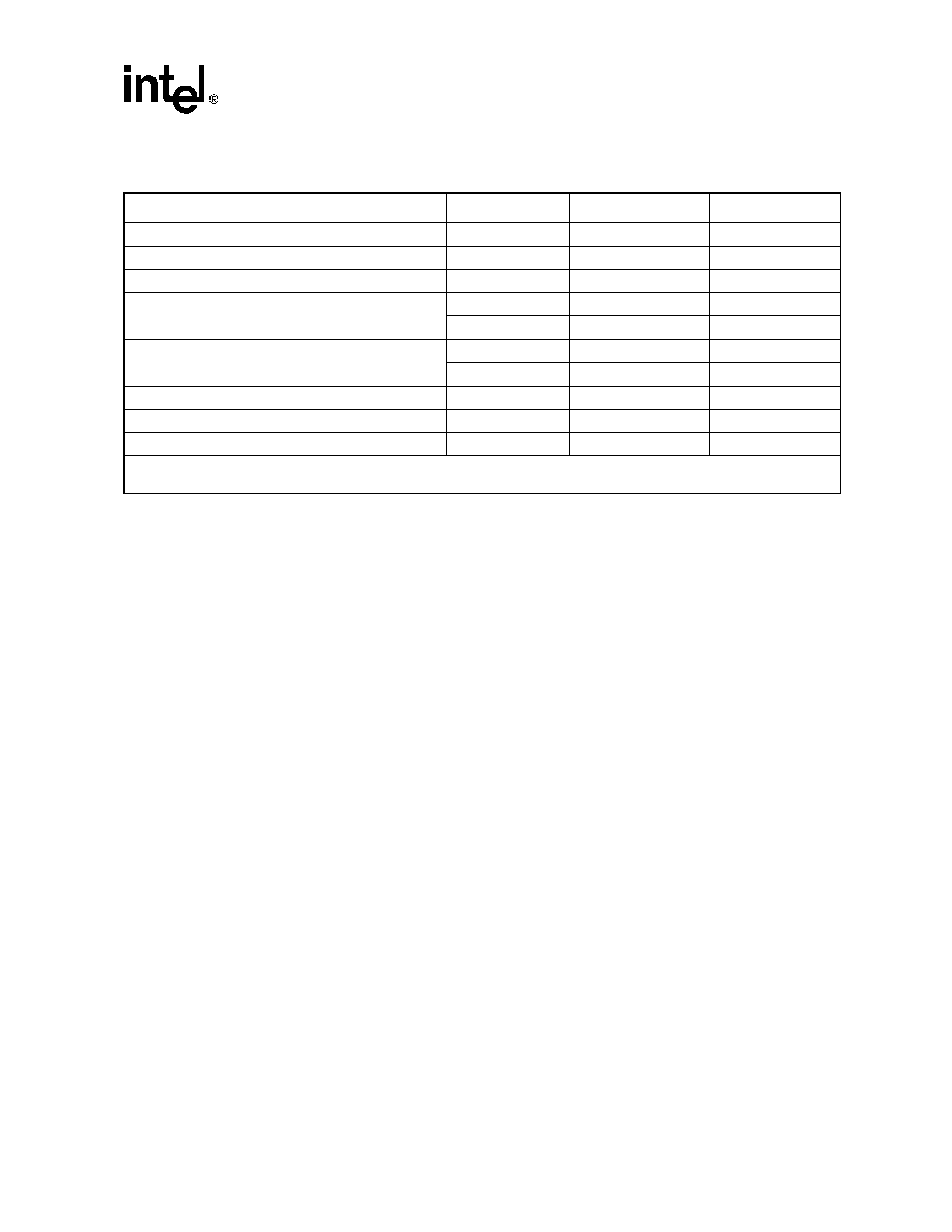
Table 2. LXT970A MII Signal Descriptions
Pin#
1
Pin Name
I/O
2,3
Signal Description
4
MII Data Interface Pins
63
62
61
60
59
TXD4
TXD3
TXD2
TXD1
TXD0
I
Transmit Data. The Media Access Controller (MAC) drives data to the
LXT970A using these inputs. TXD4 is monitored only in Symbol (5B) Mode.
These signals must be synchronized to the TX_CLK.
58
TX_EN
I
Transmit Enable. The MAC asserts this signal when it drives valid data on the
TXD inputs. This signal must be synchronized to the TX_CLK.
57
TX_CLK
I/O
Transmit Clock. Normally the LXT970A drives TX_CLK; in Slave Clock Mode,
TX_CLK is an input. Refer to the Clock Requirements discussion in the
Functional Description section on
page 18
.
25 MHz for 100 Mbps operation.
2.5 MHz for 10 Mbps operation.
56
TX_ER
I
Transmit Coding Error. The MAC asserts this input when an error has
occurred in the transmit data stream. When the LXT970A is operating at 100
Mbps, the LXT970A responds by sending invalid code symbols on the line.
46
47
48
49
50
RXD4
RXD3
RXD2
RXD1
RXD0
O
Receive Data. The LXT970A drives received data on these outputs,
synchronous to RX_CLK.
RXD4 is driven only in Symbol (5B) Mode.
51
RX_DV
O
Receive Data Valid. The LXT970A asserts this signal when it drives valid data
on RXD. This output is synchronous to RX_CLK.
55
RX_ER
O
Receive Error. The LXT970A asserts this output when it receives invalid
symbols from the network. This signal is synchronous to RX_CLK.
54
RX_CLK
O
Receive Clock. This continuous clock provides reference for RXD, RX_DV, and
RX_ER signals. Refer to the Clock Requirements discussion in the Functional
Description section.
25 MHz for 100 Mbps operation.
2.5 MHz for 10 Mbps operation.
64
COL
O
Collision Detected. The LXT970A asserts this output when detecting a
collision. This output remains High for the duration of the collision.
This signal is asynchronous and inactive during full-duplex operation.
1
CRS
O
Carrier Sense. During half-duplex operation (bit 0.8 = 0), the LXT970A asserts
this output when either transmit or receive medium is non-idle. During full-
duplex operation (bit 0.8 = 1) or repeater operation
(bit 19.13 = 1), CRS is asserted only when the receive medium is non-idle.
1. Pin numbers apply to all package types.
2. I/O Column Coding: I = Input, O = Output, OD = Open Drain, A = Analog.
3. If bit 17.3 = 0, 55
series termination resistors are recommended on all output signals to avoid undershoot/overshoot, even
on short traces.
If bit 17.3 = 1, termination resistors are not required.
4. The LXT970A supports the 802.3 MDIO register set. Specific bits in the registers are referenced using an "X.Y" notation,
where X is the register number (0-6 or 16-20) and Y is the bit number (0-15).
LXT970A -- Dual-Speed Fast Ethernet Transceiver
12
Datasheet
3
TRSTE
I
Tri-state. In DTE Mode (19.13 = 0), when TRSTE input is High, the LXT970A
isolates itself from the MII Data Interface, and controls the MDIO register bit
0.10 (Isolate bit).
When MDDIS is High, TRSTE provides continuous control over bit 0.10. When
MDDIS is Low, TRSTE sets initial (default) values only and reverts control back
to the MDIO interface.
In Repeater Mode (19.13 = 1), when TRSTE input is High, the LXT970A tri-
states the receive outputs of the MII (RXD<4:0>, RX_DV, RX_ER, RX_CLK).
MII Control Interface Pins
15
MDDIS
I
Management Disable. When MDDIS is High, the MDIO is restricted to Read
Only and the MF<4:0>, CFG<1:0>, and FDE pins provide continual control of
their respective bits. When MDDIS is Low at power up or Reset, the MF<4:0>,
CFG<1:0>, and FDE pins control only the initial or "default" values of their
respective register bits. After the power-up/reset cycle is complete, bit control
reverts to the MDIO serial channel.
45
MDC
I
Management Data Clock. Clock for the MDIO serial data channel. Maximum
frequency is 2.5 MHz.
44
MDIO
I/O
Management Data Input/Output. Bidirectional serial data channel for PHY/
STA communication.
2
FDS/MDINT
OD
Full-Duplex Status. When bit 17.1 = 0 (default), this pin indicates full-duplex
status. (High = full-duplex, Low = half-duplex)
This pin can drive a high efficiency LED. (See
Table 23
for detail specifications).
Management Data Interrupt. When bit 17.1 = 1, an active Low output on this
pin indicates status change.
Interrupt is cleared by sequentially reading Register 1, then Register 18.
Table 3. LXT970A Fiber Interface Signal Descriptions
Pin#
1
Pin Name
I/O
2
Signal Description
17
18
FIBOP
FIBON
O
Fiber Output, Positive and Negative. Differential pseudo-ECL driver pair compatible with
standard fiber transceiver for 100BASE-FX.
27
28
FIBIP
FIBIN
I
Fiber Input, Positive and Negative. Differential pseudo-ECL receive pair compatible with
standard fiber transceiver for 100BASE-FX.
1. Pin numbers apply to all package types.
2. I/O Column Coding: I = Input, O = Output, OD = Open Drain, A = Analog.
Table 2. LXT970A MII Signal Descriptions (Continued)
Pin#
1
Pin Name
I/O
2,3
Signal Description
4
1. Pin numbers apply to all package types.
2. I/O Column Coding: I = Input, O = Output, OD = Open Drain, A = Analog.
3. If bit 17.3 = 0, 55
series termination resistors are recommended on all output signals to avoid undershoot/overshoot, even
on short traces.
If bit 17.3 = 1, termination resistors are not required.
4. The LXT970A supports the 802.3 MDIO register set. Specific bits in the registers are referenced using an "X.Y" notation,
where X is the register number (0-6 or 16-20) and Y is the bit number (0-15).
Dual-Speed Fast Ethernet Transceiver -- LXT970A
Datasheet
13
Table 4. LXT970A Twisted-Pair Interface Signal Descriptions
Pin#
1
Pin Name
I/O
2
Signal Description
21
23
TPOP
TPON
AO
Twisted-Pair Output, Positive and Negative. Differential driver pair produces 802.3-
compliant pulses for either 100BASE-TX or 10BASE-T transmission.
20
TREF
AO
Transmit Reference. Tie to center tap of output transformer.
29
30
TPIP
TPIN
AI
Twisted-Pair Input, Positive and Negative. Differential input pair for either 100BASE-TX
or 10BASE-T reception.
1. Pin numbers apply to all package types.
2. I/O Column Coding: I = Input, O = Output, OD = Open Drain, A = Analog
Table 5. LXT970A LED Indicator Signal Descriptions
Pin#
1
Pin Name
I/O
2
Signal Description
3
38
LEDS
O
Speed LED. Active Low output indicates 100 Mbps operation is selected.
42
LEDR
O
Receive LED. Active Low output indicates that receiver is active.
41
LEDT
O
Transmit LED. Active Low output indicates transmitter is active.
40
LEDL
O
Link LED. Active Low output;
During 100 Mbps operation, indicates scrambler lock and receipt of valid Idle codes.
During 10 Mbps operation, indicates Link Valid status.
39
LEDC
O
Collision LED. In default mode, active Low output indicates collision. However, LEDC is
programmable and may be set for other indications. For programming options, see
Configuration Register 19 in
Table 55, "Configuration Register (Address 19, Hex 13)" on
page 71
.
1. Pin numbers apply to all package types.
2. I/O Column Coding: I = Input, O = Output, OD = Open Drain, A = Analog.
3. LEDs are read at power-up to determine scrambler seed values.
Table 6. LXT970A Miscellaneous Signal Descriptions
Pin#
1
Pin Name
I/O
2
Signal Description
10
TEST
I
Test. Must be tied Low.
12
11
XI
XO
I
O
Crystal Input and Output. Use a clock at XI or connect a 25 MHz crystal oscillator across
XI and XO. Refer to the Functional Description section for detailed clock requirements on
page 18
.
25
RBIAS
AI
Bias Control. Controls operating circuit bias via an external 22.1 k
,
1% resistor to
ground.
16
RESET
I
Reset. This active Low input is OR'ed with the control register Reset bit (0.15). The
LXT970A reset cycle is extended 300
�
s (nominal) after Reset is de-asserted.
34
PWRDWN
I
Power Down. When High, forces LXT970A into power down mode. This pin is OR'ed with
the Power Down bit (0.11). Refer to
Table 45
for more information.
32, 35,
36
N/C
-
No Connection. Leave open.
1. Pin numbers apply to all package types.
2. I/O Column Coding: I = Input, O = Output, OD = Open Drain, A = Analog.
LXT970A -- Dual-Speed Fast Ethernet Transceiver
14
Datasheet
Table 7. LXT970A Hardware Control Interface Signal Descriptions
Pin#
1
Pin Name
I/O
2
Signal Description
3
8
7
6
5
4
MF0
MF1
MF2
MF3
MF4
I
Multi-Function (MF). Five dual-function configuration inputs. Each pin accepts one of four
input voltage levels (V
MF
1 = 5V, V
MF
2 = 3.5V, V
MF
3 = 1.5V, V
MF
4 = 0V).
A simple resistor divider network, as shown in
Figure 20 on page 45
, is required to establish
Mid-level (V
MF
2 and V
MF
3) settings. V
MF
1 and V
MF
4 (default) settings, can be established
with the LXT970A standard power supply and do not require a voltage divider. One voltage
divider may be used to drive the MF pins in designs using multiple LXT970A's.
Each MF pin internally drives two different configuration functions. The first function
determines the 5-bit address that the LXT970A responds to on the MDIO line. The second
function determines a particular operational mode of the LXT970A. Each MF pin also
determines the state of a particular bit in the MII registers. The MDDIS input determines if this
effect occurs only at initialization (MDDIS = 0) or continuously (MDDIS = 1). The relationship
between the input levels and the two configuration functions are shown in
Table 8 on page 16
and
Table 9 on page 17
.
The operating functions of MF4, CFGO, and CFG1 change depending on the state of MF0
(Auto-Negotiation enabled or disabled). The functions of MF4, CFG1 and FDE are
interrelated.
The functions of the five MF inputs are as follows:
1. Pin numbers apply to all package types.
2. I/O Column Coding: I = Input, O = Output, OD = Open Drain, A = Analog.
3. FDE, CFG0, and CFG1 are affected by the MDDIS input pin. When MDDIS = 0, these inputs determine only the initial state
of the function they control. When MDDIS = 1, these inputs provide continuous hardware control over their corresponding
functions.
Pin
MII Address
MII Bit
Operating Function
MF0
0
0.12
Auto-Negotiation
MF1
1
19.13
Repeater Mode (Disabling DTE Mode)
MF2
2
19.4
5B Symbol Mode (Disabling 4B Nibble Mode)
MF3
3
19.3
Scrambler Operation (Disabling Scrambler)
MF4
4
4.7
4.8
Auto-Negotiation Enabled - Advertise 100 Mbps
19.2
Auto-Negotiation Disabled - Selects TX/FX

Dual-Speed Fast Ethernet Transceiver -- LXT970A
Datasheet
15
13
FDE
I
Full-Duplex Enable.
When A/N is enabled, FDE determines full-duplex advertisement capability in combination
with MF4 and CFG1.
When A/N is disabled, FDE directly affects full-duplex operation and determines the value of
bit 0.8 (Duplex Mode).
When FDE is High, full-duplex is enabled and 0.8 = 1.
When FDE is Low, full-duplex is disabled and 0.8 = 0.
14
CFG0
I
Configuration Control 0.
When A/N is enabled, Low-to-High transition on CFG0 causes auto-negotiate to re-start and
0.9 = 1.
When A/N is disabled, this input selects operating speed and directly affects bit 0.13.
When CFG0 is High, 100 Mbps is selected and 0.13 = 1. If FX Operation is selected, this
input must be tied High.
When CFG0 is Low, 10 Mbps is selected and 0.13 = 0.
33
CFG1
I
Configuration Control 1.
When A/N is enabled, CFG1 determines operating speed advertisement capabilities in
combination with MF4.
When A/N is disabled, CFG1 enables 10 Mbps link test function and directly affects bit 19.8.
When CFG1 is High, 10 Mbps link test is disabled and 19.8 = 1.
When CFG1 is Low, 10 Mbps link test is enabled and 19.8 = 0.
Table 7. LXT970A Hardware Control Interface Signal Descriptions (Continued)
Pin#
1
Pin Name
I/O
2
Signal Description
3
1. Pin numbers apply to all package types.
2. I/O Column Coding: I = Input, O = Output, OD = Open Drain, A = Analog.
3. FDE, CFG0, and CFG1 are affected by the MDDIS input pin. When MDDIS = 0, these inputs determine only the initial state
of the function they control. When MDDIS = 1, these inputs provide continuous hardware control over their corresponding
functions.

LXT970A -- Dual-Speed Fast Ethernet Transceiver
16
Datasheet
Table 8
summarizes the relationship between input voltage levels (V
MF
1, V
MF
2, V
MF
3, V
MF
4) and
the configuration function for each of the MF input pins. Each MF pin shows two configuration
inputs; configuration function and MII address. The initial setting of the corresponding bit is also
shown.
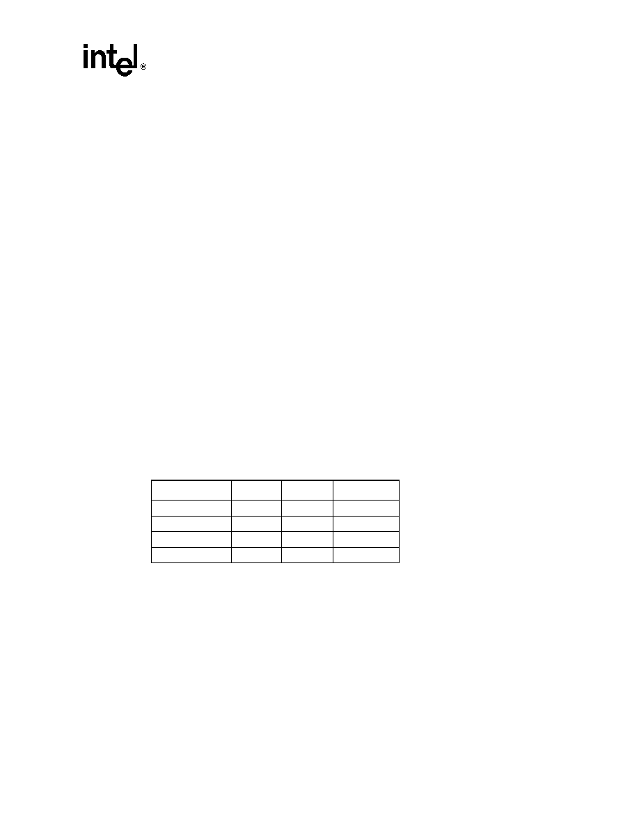
Table 8. MF Pin Function Settings
1, 3
Input Voltage Levels
2
Pin
Function
V
MF
1 (5V)
V
MF
2 (3.5V)
V
MF
3 (1.5V)
V
MF
4 (0V)
MF0
MII Address Bit 0
1
1
0
0
Auto-Negotiation
Sets the initial value of bit
0.12
Disabled
(0.12 = 0)
Enabled
(0.12 = 1)
Enabled
(0.12 = 1)
Disabled
(0.12 = 0)
MF1
MII Address Bit 1
1
1
0
0
Repeater / DTE Mode
Sets the initial value of bit
19.13
DTE
(19.13 = 0)
Repeater
(19.13 = 1)
Repeater
(19.13 = 1)
DTE
(19.13 = 0)
MF2
MII Address Bit 2
1
1
0
0
Nibble (4B) / Symbol (5B) Mode
Sets the initial value of bit
19.4
Nibble (4B)
(19.4 = 0)
Symbol (5B)
(19.4 = 1)
Symbol (5B)
(19.4 = 1)
Nibble (4B)
(19.4 = 0)
MF3
MII Address Bit 3
1
1
0
0
Scrambler Operation
Sets the initial value of bit
19.3
Enabled
(19.3 = 0)
Bypassed
(19.3 = 1)
Bypassed
(19.3 = 1)
Enabled
(19.3 = 0)
MF4
MII Address Bit 4
1
1
0
0
If Auto-Negotiate Enabled via
MF0, MF4 works in combination
with CFG1 to control operating
speed and duplex advertisement
capabilities via bits 4.5 - 4.8.
See
Table 9
for details.
If Auto-Negotiate Disabled via
MF0, MF4 selects either
TX or FX Mode
Sets the initial value of bit
19.2
100TX
(19.2 = 0)
100FX
(19.2 = 1)
100FX
(19.2 = 1)
100TX
(19.2 = 0)
1. In MDIO Control Mode, the MF pins control only the initial or default value for the respective register bits. In Manual Control
mode, the MF pins provide continuous control of the respective register bits.
2. Input Voltage Levels (V
MF
1, V
MF
2, V
MF
3, V
MF
4) for MF pins.
3. See
Table 12
through
Table 14
for operating configuration set-up.

Dual-Speed Fast Ethernet Transceiver -- LXT970A
Datasheet
17
Table 9. LXT970A Auto-Negotiation Operating Speed/Full-Duplex
Advertisement Settings
Desired Configuration
Input Value
MDIO Registers
MF4 CFG1
FDE
Advertise all capabilities
Ignore FDE
V
MF
1, V
MF
4 Low
�
Sets 4.5, 4.6, 4.7 and 4.8 = 1
Advertise 10 Mbps only
Advertise FD
V
MF
1, V
MF
4 High
High
Sets 4.5 = 1
Sets 4.7 and 4.8 = 0
Sets 4.6 = 1
Advertise 10 Mbps only
Do Not Advertise FD
Low
Sets 4.5 = 1
Sets 4.7 and 4.8 = 0
Sets 4.6 = 0
Advertise 100 Mbps only
Advertised FD
V
MF
2, V
MF
3 Low
High
Sets 4.7 = 1
Sets 4.5 and 4.6 = 0
Sets 4.8 = 1
Advertise 100 Mbps only
Do Not Advertise FD
Low
Sets 4.7 = 1
Sets 4.5 and 4.6 = 0
Sets 4.8 = 0
Advertise 10/100 Mbps
Advertise FD
V
MF
2, V
MF
3 High
High
Sets 4.5 and 4.7 = 1
Sets 4.6 and 4.8 = 1
Advertise 10/100 Mbps
Do Not Advertise FD
Low
Sets 4.5 and 4.7 = 1
Sets 4.6 and 4.8 = 0
LXT970A -- Dual-Speed Fast Ethernet Transceiver
18
Datasheet
2.0
Functional Description
2.1
Introduction
The LXT970A, a new-generation version of the LXT970 10/100 PHY Fast Ethernet Transceiver
incorporates several functional enhancements for a more robust Ethernet solution. The LXT970A
supports optional MII driver strength capabilities and link-loss criteria selectable via the MDIO
register set.
The LXT970A can directly drive a twisted-pair cable for up to 100 meters. The LXT970A also
provides a pseudo-ECL interface for driving a 100BASE-FX fiber connection. On power-up, the
LXT970A uses auto-negotiation with parallel detection to automatically determine line operating
conditions. If the PHY device on the other side of the link supports auto-negotiation, the
LXT970A auto-negotiates using Fast Link Pulse (FLP) bursts. If the PHY partner does not support
auto-negotiation, the LXT970A automatically detects the presence of either link pulses (10 Mbps
PHY) or Idle symbols (100 Mbps PHY) and set its operating speed accordingly. When the line
speed selection is made via the parallel detection method, the duplex mode sets to half. The user
may later select full-duplex operation by subsequent writes to the appropriate MDIO register. Line
operation can also be set using the Hardware Control Interface.
The LXT970A interfaces to a 10/100 MAC through the MII interface. The LXT970A performs all
functions of the Physical Coding Sublayer (PCS) and Physical Media Attachment (PMA) sublayer
as defined in the IEEE 802.3 100BASE-X specification. It also performs all Physical Media
Dependent (PMD) sublayer functions for 100BASE-TX connections. The MII speed is
automatically set once line operating conditions have been determined.
See
Figure 3
for a typical Network Interface Card (NIC). The LXT970A supports NIC, repeater,
and switch applications. It provides half- and full-duplex operation at 100 Mbps and 10 Mbps. The
LXT970A supports the 802.3 MDIO register set. Specific bits in the registers are referenced using
an "X.Y" notation, where X is the register address (0-6 or 16-20) and Y is the bit number (0:15).
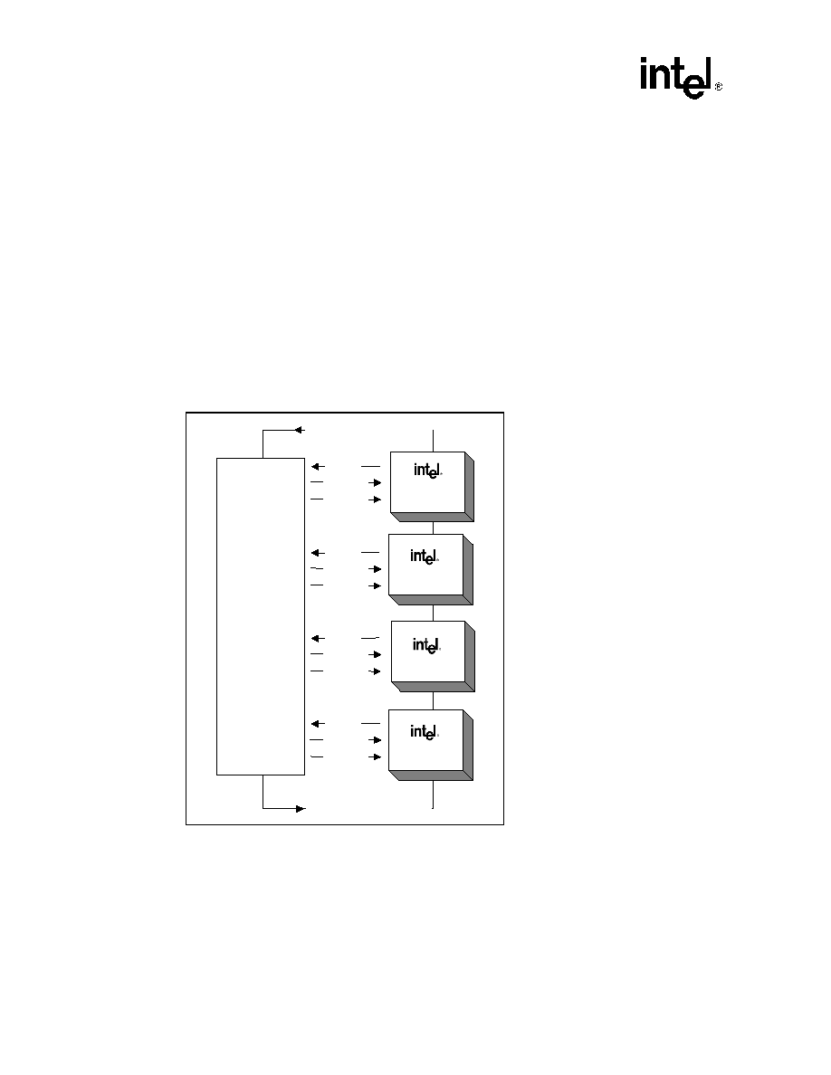
Figure 3. Network Interface Card (NIC) Application
PC Bus (EISA,PCI)
MAC Controller
LXT970A
Magnetic
RJ-45
Connection

Dual-Speed Fast Ethernet Transceiver -- LXT970A
Datasheet
19
2.2
Interfaces (Network Media/Protocol Support)
The LXT970A provides the following interfaces:
�
A Twisted-Pair Interface which directly supports 100BASE-TX and 10BASE-T applications.
�
A pseudo-ECL (PECL) Fiber Interface which supports 100BASE-FX applications through an
external fiber transceiver.
�
An MII (Media Independent Interface) for interfacing 10/100 Media Access Controllers
(MACs).
�
A Hardware Control Interface to configure various operating characteristics.
2.2.1
Twisted-Pair Interface
The Twisted-Pair Interface directly supports both 100BASE-TX and 10BASE-T applications. The
interface is capable of directly driving an RJ-45 interface through magnetics and termination
resistors. The interface uses two signal pairs - one for transmit and one for receive. A third output,
TREF, connects to the center-tap of the transmit transformer. The same signal pairs, magnetics, and
termination resistors are used for both 10 and 100 Mbps operation.
When the LXT970A is operating as a 100 Mbps device, it transmits and receives a 125 Mbps, 5B-
encoded, scrambled MLT-3 waveform on this interface. The MLT-3 waveform is continuous.
When there is no data to send, "IDLE" symbols are sent and received.
When the LXT970A is operating as a 10 Mbps device, it transmits and receives 10 Mbps
Manchester-encoded data. The waveform is not continuous. When there is no data to send, the
line is left in an idle state. Link pulses are transmitted periodically to keep the link up.
The LXT970A supports both fixed operation and auto-negotiation with parallel detection on this
interface. Fixed operation allows the designer to specify the line speed and duplex mode. With
auto-negotiation enabled, the LXT970A automatically determines line speed and duplex state by
exchanging capability "pages" with its link partner.
A 4 k
passive load is always present across the twisted-pair inputs. When enabled, the twisted-
pair inputs are actively biased to approximately 2.8V.
In applications where the Twisted-Pair Interface is not used, the inputs and outputs may be left
unconnected.
The Twisted-Pair Interface is disabled in power down mode, when the Fiber Interface is selected,
or when the transmit disconnect (bit 19.0) is set. When the Twisted-Pair Interface is disabled its
outputs are tri-stated and inputs are unbiased.
2.2.2
Fiber Interface
The pseudo-ECL Fiber Interface is suitable for driving 100BASE-FX applications through an
external fiber transceiver. This interface consists of a transmit and receive pair. The LXT970A
sends and receives a continuous 125 Mbps, 5B-encoded NRZI stream on this interface.
Scrambling and MLT-3 are not used in fiber connections.
There is no industry standard for auto-negotiation on 100BASE-FX. The LXT970A only supports
forced operation on the Fiber Interface. The LXT970A does not support 10FL (10 Mbps fiber)
applications.
LXT970A -- Dual-Speed Fast Ethernet Transceiver
20
Datasheet
The LXT970A does not support the Signal Detect Function. However, the PMA functions of the
LXT970A guarantee that it will detect invalid link conditions and break down a link, even without
the Signal Detect function.
In applications where the Fiber Interface is not used, the inputs and outputs may be left
unconnected. The Fiber Interface is disabled in power down mode and when the Twisted-Pair
Interface is enabled. When the Fiber Interface is disabled its outputs are pulled to ground.
2.2.3
MII Interface
The LXT970A implements the Media Independent Interface (MII) as defined in the IEEE 802.3.
This interface consists of a data interface and a management interface as shown in
Figure 4
. The
data interface is used for exchanging data between a 10/100 802.3 compliant Ethernet Media
Access Controller (MAC) and the LXT970A. The management portion of the interface allows
network management functions to control and monitor the LXT970A.
2.2.3.1
Selectable Driver Levels
The LXT970A supports two options for driver-strength capabilities that can be selected via bit
17.3.
High-strength (bit 17.3 = 0, default) MII driver level can effectively source 50 - 60 mA. To avoid
undershoot or overshoot, series termination resistors are recommended on all output signals when
this driver level is selected.
Reduced (bit 17.3 = 1) MII driver level relaxes the pull-down strength of the MII signals by a
factor of ten and the pull-up strength by a factor of eight. Termination resistors are not required on
the MII outputs when this driver level is selected.
Figure 4. MII Interface
LXT970A
Media Access Controller
Media Independent
Interface (MII)
Data
Mgmt
Dual-Speed Fast Ethernet Transceiver -- LXT970A
Datasheet
21
2.2.3.2
MII Data Interface
Figure 5
shows the data portion of the MII interface. Separate channels are provided for
transmitting data from the MAC to the LXT970A (TXD), and for receiving data (RXD) from the
line.
Each channel has its own clock, data bus and control signals. The LXT970A supplies both clock
signals as well as separate outputs for carrier sense and collision.
Normal data transmission across the MII is implemented in 4-bit wide nibbles known as 4B Nibble
Mode. In 5B Symbol Mode, a fifth bit allows 5-bit symbols to be sent across the MII. Refer to the
100 Mbps Operation section on
page 32
for additional information.
Transmit Clock
The transmit clock (TX_CLK) is normally generated by the LXT970A from the master 25 MHz
reference source at the XI input. However, when the XI input is grounded, TX_CLK becomes the
master reference clock input.
The transmit data and control signals must always be synchronized to TX_CLK by the MAC. The
LXT970A normally samples these signals on the rising edge of TX_CLK. However, Advanced
TX_CLK Mode is available by setting MII register bit 19.5=1. In this mode, the LXT970A
samples the transmit data and control signals on the falling edge of TX_CLK.
Further details of clock modes can be found in the Operating Requirements section on
page 27
.
Receive Clock
The source of the receive clock varies depending on operating conditions. For 100BASE-TX and
100BASE-FX links, receive clock is continuously recovered from the line. If the link goes down,
and auto-negotiation is disabled, receive clock operates off the master input clock (XI or
TX_CLK).
For 10T links, receive clock is recovered from the line while carrier is active and operates from the
master input clock when the line is idle.
Figure 5. MII Data Interface
LXT970A
Media Access
Controller
MAC
RX_CLK
RXD<3:0>
RX_DV
RX_ER
TX_CLK
TXD<3:0>
TX_EN
TX_ER
CRS
COL

LXT970A -- Dual-Speed Fast Ethernet Transceiver
22
Datasheet
The LXT970A synchronizes the receive data and control signals to RX_CLK. The LXT970A
always changes these signals on the falling edge of RX_CLK in order to stabilize the signals at the
rising edge of the clock with 10 ns setup and hold times.
Transmit Enable
The MAC must assert TX_EN the same time as the first nibble of preamble, and de-assert TX_EN
after the last bit of the packet.
Receive Data Valid
The LXT970A asserts RX_DV when it receives a valid packet. Timing changes depend on line
operating speed and MII mode:
�
For 100TX and 100FX links with the MII in 4B mode, RX_DV is asserted from the first nibble
of preamble to the last nibble of the data packet.
�
For 100TX and 100FX links with the MII in 5B mode, RX_DV is asserted starting with the /K
symbol and ending with the /T symbol.
�
For 10BT links, the entire preamble is truncated. RX_DV is asserted with the first nibble of
the SFD "5D" and remains asserted until the end of the packet.
Error Signals
In 100TX mode, when the LXT970A receives an errored symbol from the network, it asserts
RX_ER and drives "1110" (4B) or "01110" (5B) on the RXD pins.
When the MAC asserts TX_ER, the LXT970A drives "H" symbols out on the line.
There are no error functions in 10T mode.
Carrier Sense
Carrier sense (CRS) is an asynchronous output. It is always generated when a packet is received
from the line and in some modes when a packet is transmitted.
On transmit CRS is asserted on a 10BT, half-duplex link when MII Register 19.11 = 0 (default
state), or on any 100 Mbps half-duplex link. Carrier sense is not generated on transmit when the
link operation is full-duplex, or with 10BT half-duplex links when 19.11=1.
Usage of CRS for Interframe Gap (IFG) timing is not recommended for the following reasons:
�
De-assertion time for CRS is slightly longer than assertion time. This causes the IFG interval
to appear somewhat shorter to the MAC than it actually is on the wire.
�
CRS de-assertion is not aligned with TX_EN de-assertion on transmit loopbacks in half-
duplex mode.
Operational Loopback
Operational loopback is provided for 10 Mbps half-duplex links when bit 19.11 = 0. Data
transmitted by the MAC will be looped back on the receive side of the MII. Operational loopback
is not provided for 100 Mbps links, full-duplex links, or when 19.11 = 1.
Dual-Speed Fast Ethernet Transceiver -- LXT970A
Datasheet
23
Test Loopback
A test loopback function is provided for diagnostic testing of the LXT970A. During test loopback
the twisted-pair interface is disabled. Data transmitted by the MAC is internally looped back by
the LXT970A and returned to the MAC.
Test loopback is available for 100 Mbps and 10 Mbps operation. Loopback paths for the two modes
of operation are shown in
Figure 6
.
Test loopback is enabled by setting bit 0.14 = 1 (loopback), bit 0.8 = 1 (full-duplex), and bit 0.12 =
0 (disable auto-negotiation). The desired mode of operation for test loopback is set using bits 0.13
and 19.2 as shown in
Table 10
.
Collision
The LXT970A asserts its collision signal, asynchronously to any clock, whenever the line state is
half-duplex and the transmitter and receiver are active at the same time.
Table 11
summarizes the
conditions for assertion of carrier sense, collision, and data loopback signals.
Table 10. Test Loopback Operation
Mode of Operation
Bit
19.2
0.13
10 Mbps Test Loopback
0
0
100 Mbps Test Loopback
1
1
1. Also set bit 0.14 = 1, bit 0.8 = 1, and 0.12 = 0 to enable Test
Loopback.
Figure 6. Loopback Paths
Digital
Block
MII
Analog
Block
FX
Driver
TX
Driver
100 Mbps
Loopback
10 Mbps
Loopback
Table 11. Carrier Sense, Loopback, and Collision Conditions
Speed & Duplex Condition
Carrier Sense
Operational
Loopback
Collision
Full-Duplex at 10 Mbps or 100 Mbps
Repeater Mode
Receive only
None
None
100 Mbps, Half-Duplex
Transmit or Receive
None
Transmit and Receive
10 Mbps, Half-Duplex, 19.11 = 0
Transmit or Receive
Yes
Transmit and Receive
10 Mbps, Half-Duplex, 19.11 = 1
Receive only
None
Transmit and Receive
LXT970A -- Dual-Speed Fast Ethernet Transceiver
24
Datasheet
2.2.3.3
Repeater Mode
The LXT970A MII normally operates in DTE Mode (19.13 = 0). An alternative operating mode is
available for repeater applications (19.13 = 1).
In Repeater Mode, the Carrier Sense (CRS) and Tri-state (TRSTE) signals request and grant bus
access. The TRSTE pin controls only the receive channel of the MII (RX_DV, RX_ER, RX_CLK,
and RXD).
As shown in
Figure 7
, a central Repeater State Machine (RSM) is required to perform arbitration
and determine which LXT970A drives the MII Data Interface. The RSM is responsible for
enforcing collisions, and ensuring packets are not transmitted to the port they were received from.
This is accomplished by supplying each LXT970A with individual TX_EN outputs. Although
repeater operation is half-duplex, the LXT970A operates the MII as a full-duplex interface in
Repeater Mode. CRS is generated only on receive and Collision (COL) is never generated.
Repeater Mode is normally used with Slave Clock Mode (XI = GND and TX_CLK is an input).
2.2.3.4
MII Management Interface
The LXT970A supports the IEEE 802.3 MII Management Interface also known as the
Management Data Input/Output (MDIO) Interface. This interface allows upper-layer devices to
monitor and control the state of the LXT970A. MDIO interface consists of a physical connection, a
specific protocol which runs across the connection, and an internal set of addressable registers. The
physical interface consists of a data line (MDIO) and clock line (MDC), a control line (MDDIS)
Figure 7. Repeater Block Diagram
Repeater
State Machine
(RSM)
CRS
TRSTE
TX_EN
CRS
TRSTE
TX_EN
CRS
TRSTE
TX_EN
CRS
TRSTE
TX_EN
Receive Channel (RXD)
Transmit Channel (TXD)
LXT970A
LXT970A
LXT970A
LXT970A
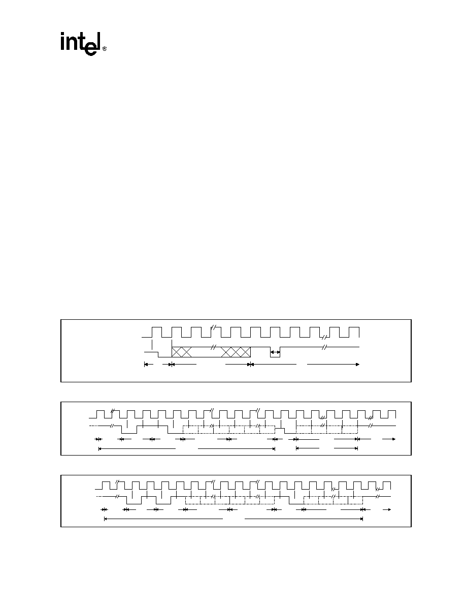
Dual-Speed Fast Ethernet Transceiver -- LXT970A
Datasheet
25
and an optional interrupt line (MDINT). The LXT970A can signal an interrupt using the MDIO
signal as shown in
Figure 8
. The user can also assign a separate pin for this function. If bit 17.1 = 1,
pin 2 (FDS/MDINT) will be used as an MDINT pin.
The protocol allows one controller to communicate with multiple LXT970A devices. The MF pins
control one bit each of the 5-bit address setting. Each LXT970A is assigned an MII address
between 0 and 31. Details of the MF inputs are shown in
Table 7 on page 14
. Timing for the MDIO
Interface is shown in
Table 42 on page 61
. Read and write operations are shown in
Figure 9
and
Figure 10
. Operation of this interface is controlled by the MDDIS input pin. When MDDIS is High,
the MDIO operates as a read-only interface. When MDDIS is Low, read and write are enabled.
The LXT970A supports twelve 16-bit MDIO registers. Registers 0-6 are required and their
functions are specified by the IEEE 802.3 specification. Additional registers are included for
expanded functionality. The MDIO Register set for the LXT970A is described in
Table 45
through
Table 56
. Specific bits in the registers are referenced using an "X.Y" notation, where X is the
register number (0-6 or 16-20) and Y is the bit number (0-15).
MII Management Interrupt
The MDINT/FDS pin functions as a management data interrupt on the MII when 17.1 = 1. An
active Low on this pin indicates a status change on the LXT970A. The interrupt is activated when
changes are made to the following conditions:
�
Link Status
�
Duplex Status
This interrupt is cleared by sequentially reading Register 1 and Register 18.
Figure 8. MDIO Interrupt Signaling
Figure 9. Management Interface - Read Frame Structure
Figure 10. Management Interface - Write Frame Structure
MDC
MDIO
Interrupt
Turn
Around
Z
Idle
0
INT
Read Data
Sourced by
LXT970A
MDIO FRAME
MDC
MDIO
(Read)
32 "1"s
0
1
1
0
Preamble
SFD
Op Code
PHY Address
Turn
Around
Z
0
A4
A3
A0
R4
R3
R0
Register Address
D15
D14
D1
Data
Idle
Write
Read
D15
D14
D1
D0
Idle
MDC
MDIO
(Write)
32 "1"s
0
1
0
1
Preamble
SFD
Op Code
PHY Address
Turn
Around
1
0
A4
A3
A0
R4
R3
R0
Register Address
D15
D14
D1
D0
Data
Idle
Idle
Write
LXT970A -- Dual-Speed Fast Ethernet Transceiver
26
Datasheet
2.2.4
Hardware Control Interface
The Hardware Control Interface consists of MF<4:0>, CFG <1:0> and FDE input pins. This
interface is used to configure operating characteristics of the LXT970A and to determine the
MDIO Address. When MDDIS is Low, the Hardware Control Interface provides initial values for
the MDIO registers, and then passes control to the MDIO Interface.
When MDDIS is High, the Hardware Control Interface provides continuous control over the
LXT970A. Individual chip addressing allows multiple LXT970A devices to share the MII in either
mode.
Table 12
,
Table 13
and
Table 14
show how to set up the desired operating configurations
using the Hardware Control Interface.
.
Table 12. Configuring the LXT970A via Hardware Control
Desired Configuration
Pin Name
Voltage Level
MDIO Registers
Auto-Negotiation Enabled
1
MF0
V
MF
2, V
MF
3
0.12 = 1
Auto-Negotiation Disabled
2
MF0
V
MF
1, V
MF
4
0.12 = 0
Normal Operation
(DTE Mode, Nibble Mode, Scrambler Enabled)
MF1
MF2
MF3
V
MF
1, V
MF
4
19.13 = 0
19.4 = 0
19.3 = 0
Repeater Mode
MF1
V
MF
2, V
MF
3
19.13 = 1
Symbol Mode
MF2
V
MF
2, V
MF
3
19.4 = 1
Scrambler Bypass Mode
MF3
V
MF
2, V
MF
3
19.3 = 1
1. Refer to
Table 13
for Hardware Control Interface functions available when auto-negotiation is enabled.
2. Refer to
Table 14
for Hardware Control Interface functions available when auto-negotiation is disabled.
Table 13. LXT970A Operating Configurations / Auto-Negotiation Enabled
Desired
Configuration
1,2
Input Value
MDIO Registers
MF4
CFG1
FDE
4.5
4.6
4.7
4.8
Advertise All
V
MF
1, V
MF
4
Low
Ignore
1
1
1
1
Advertise 100 HD
V
MF
2, V
MF
3
Low
Low
0
0
1
0
Advertise 100 HD/FD
V
MF
2, V
MF
3
Low
High
0
0
1
1
Advertise 10 HD
V
MF
1, V
MF
4
High
Low
1
0
0
0
Advertise 10 HD/FD
V
MF
1, V
MF
4
High
High
1
1
0
0
Advertise 10/100 HD
V
MF
2, V
MF
3
High
Low
1
0
1
0
Advertise 10/100 HD/FD
V
MF
2, V
MF
3
High
High
1
1
1
1
1. Refer to
Table 12
for basic configurations.
2. Refer to
Table 14
for Hardware Control Interface functions available when auto-negotiation is disabled.
Dual-Speed Fast Ethernet Transceiver -- LXT970A
Datasheet
27
2.3
Operating Requirements
2.3.1
Power Supply Requirements
The LXT970A requires a 5V power supply. Power should be supplied from a single source to the
VCC, VCCA, VCCT, and VCCR power pins. A ground return path must be provided to the GND,
GNDA, GNDT, and GNDR pins. As a matter of practice, the power supply should be as clean as
possible. Filtering is recommended for the analog power pins (VCCA, VCCT, VCCR) at least in
the initial design. Consult the Design Recommendations section on
page 42
for details. A
decoupling capacitor is recommended between each VCC pin and its respective GND, placed as
close to the device as possible.
2.3.1.1
Optional MII Power Supply
The MII may be powered by either a 3.3V or 5V source via the VCCIO pin. To avoid power
sequencing issues, the VCCIO pin should be supplied from the same source used to power the
other side of the MII interface. When VCCIO is supplied with 3.3V, the MII inputs are not tolerant
of 5V signal levels. The MDIO and MDC pins must be operated at the same voltage as the rest of
the MII interface.
2.3.2
Reference Clock Requirements
The LXT970A requires a continuous, stable reference clock. There are two clock modes, Master
Clock Mode and Slave Clock Mode. Depending on the mode of operation, the clock may be
supplied at the crystal oscillator pins (XI, XO), or at the Transmit Clock pin (TX_CLK). See
Table
25 on page 48
for input clock requirements.
Table 14. LXT970A Operating Configurations / Auto-Negotiation Disabled
Desired Configuration
1,2
Pin Name
Input Value
MDIO Registers
Force 100FX Operation
MF4
V
MF
2, V
MF
3
19.2 = 1
CFG0
High
0.13 = 1
MF3
V
MF
1, V
MF
4
19.3 = 0
Force 100TX Operation
MF4
V
MF
1, V
MF
4
19.2 = 0
CFG0
High
0.13 = 1
Force 10T Operation
MF4
V
MF
1, V
MF
4
19.2 = 0
CFG0
Low
0.13 = 0
Force Full-Duplex Operation
FDE
High
0.8 = 1
Disable 10T Link Test
CFG1
High
19.8 = 1
Enable 10T Link Test
CFG1
Low
19.8 = 0
1. Refer to
Table 12
for basic configurations.
2. Refer to
Table 13
for Hardware Control Interface functions available when auto-negotiation is enabled.

LXT970A -- Dual-Speed Fast Ethernet Transceiver
28
Datasheet
2.3.2.1
Master Clock Mode
The Master Clock mode is recommended in most Network Interface Cards (NICs) and switch
applications. In Master Clock mode the LXT970A is the master clock source for data transmission,
and requires a 25 MHz reference signal at XI. The reference clock may be supplied either from a
crystal oscillator or from a digital clock circuit with the following specifications:
�
A frequency of 25 MHz +/-100 ppm
�
40/60 duty cycle or better
�
CMOS voltage levels (V
OH
>3.2V).
In Master Clock Mode, TX_CLK is an output and the LXT970A automatically sets the speed of
TX_CLK to match line conditions. If the line is operating at 100 Mbps, TX_CLK will be set to 25
MHz. If the line is operating at 10 Mbps, TX_CLK will be set to 2.5 MHz.
External Crystal
A crystal is typically used in NIC applications. If using a crystal oscillator, it should be
fundamental-mode and parallel-resonant, with a drive capacity of at least 7 pF. Attach between the
XI and XO pins. Add compensating capacitors between each leg and digital ground. The correct
value to use is the nominal drive capacity of the crystal minus 3 pF (input capacitance of the XI and
XO pins). One crystal can be used to drive two LXT970As. Connect the XO pin of only one 970
to one side of the crystal, and connect the other side to both XI pins. Calculate compensation
accordingly.
External Clock
An external 25 MHz clock source, rather than a crystal, is frequently used in switch applications.
When a clock is supplied to XI, XO is left open.
TX Clock Advance Mode
When operating in Master Clock mode under MDIO Control, the user can advance the transmit
clock relative to TXD<4:0> and TX_ER. When TX_CLK Advance is selected, the LXT970A
clocks TXD data in on the falling edge of TX_CLK, instead of the rising edge.
This mode provides an increase in timing margins of TXD, relative to TX_CLK. TX_CLK
Advance is enabled when bit 19.5 = 1.
2.3.2.2
Slave Clock Mode
The Slave Clock mode is typically used for repeater applications, where the LXT970A is not the
master clock source for data transmissions. In Slave Clock Mode, a digital clock circuit with TTL
levels (V
OH
>2.4V) must supply the TX_CLK input. The frequency may be either 25 MHz or 2.5
MHz. Either frequency can be used during auto-negotiation. However, once link is established,
the supplied frequency must match the link state. A 25 MHz clock must be supplied for correct
operation of a 100TX or 100FX link, and a 2.5 MHz clock must be supplied for correct operation
of a 10BT link. In Slave Clock mode, XI is connected to ground and XO is left open.
Dual-Speed Fast Ethernet Transceiver -- LXT970A
Datasheet
29
2.3.3
Bias Circuit Requirements
A 22.1 k
1% resistor must be tied between the RBIAS input and ground. High-speed signals
should be kept away from this resistor. Follow the layout recommendations given in the Design
Recommendations section on
page 42
.
2.4
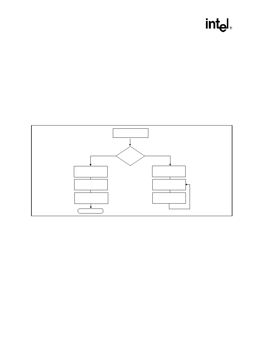
Initialization
At power-up or reset, the LXT970A performs the initialization sequence shown in
Figure 11
.
2.4.1
Control Mode Selection
Mode control selection is provided via the MDDIS pin as shown in
Table 15
. When pin 15
(MDDIS) is High, the LXT970A enters Manual Control Mode. When MDDIS is Low, MDIO
Control Mode is enabled.
2.4.1.1
MDIO Control Mode
In the MDIO Control mode, the LXT970A reads the Hardware Control Interface pins to set the
initial (default) values of the MDIO registers. Once the initial values are set, bit control reverts to
the MDIO interface.
2.4.1.2
Manual Control Mode
In the Manual Control Mode, LXT970A disables direct write operations to the MDIO registers via
the MDIO Interface. The LXT970A continuously monitors the Hardware Control Interface pins
and updates the MDIO registers accordingly.
2.4.2
Link Configuration
When the LXT970A is first powered on, reset, or encounters a link failure state, it must determine
the line speed and operating conditions to use for the network link. The LXT970A first checks the
MDIO registers (initialized via the Hardware Control Interface or MDIO Interface) for operating
instructions. Both control modes allow the user to either force the LXT970A to a specific
configuration or allow it to auto-negotiate the optimum configuration with its link partner.
Table 15. Mode Control Settings
Mode
MDDIS
RESET
PWRDWN
MDIO Control
Low
High
Low
Manual Control
High
High
Low
Reset
-
Low
Low
Power Down
-
-
High
LXT970A -- Dual-Speed Fast Ethernet Transceiver
30
Datasheet
2.4.2.1
Manual Configuration
The LXT970A can be manually configured to force operation in the following modes:
�
100FX, full-duplex
�
100FX, half-duplex
�
100TX, full-duplex
�
100TX, half-duplex
�
10T, full-duplex
�
10T, half-duplex
Refer to
Table 12
through
Table 14
in the Hardware Control Interface discussion for specific
manual configuration settings.
2.4.2.2
Auto-Negotiation/Parallel Detection
With auto-negotiation enabled at power-up or reset, the LXT970A attempts to establish link
operating conditions with its partner by sending Fast Link Pulse (FLP) bursts.
If the link partner is also capable of auto-negotiation, the two devices exchange FLP bursts to
communicate their capabilities to each other. Each side finds the highest common capabilities that
both sides can support and then begins operating in that mode.
If the link partner is not capable of auto-negotiation, it transmits either 10 Mbps Normal Link
Pulses (NLP) or 100 Mbps Idle symbols. When the LXT970A detects either NLPs or Idle symbols,
it automatically configures to match the detected operating speed in half-duplex mode. This ability
allows the LXT970A to communicate with devices that do not support auto-negotiation.
Figure 11. LXT970A Initialization Sequence
Power-up or Reset
Check Value
MDDIS
High
Low
MDIO Control
Mode
Exit
Manual Control
Mode
Disable MDIO Writes
Read H/W Control
Interface
Initialize MDIO Registers
Read H/W Control
Interface
Pass Control to MDIO
Interface
Update MDIO Registers
Dual-Speed Fast Ethernet Transceiver -- LXT970A
Datasheet
31
Controlling Auto-Negotiation
When auto-negotiation is controlled by software, the following steps are recommended:
�
After a reset or power-up (initial or from power down mode), the power down recovery time
(refer to
Table 43 on page 62
) must be exhausted before proceeding.
�
Set MDIO Register 4 advertisement capabilities before setting MDIO bit 0.12 = 1 to enable
auto-negotiation.
2.5
Monitoring Operational Status
2.5.1
Monitoring Status via MII Registers
The Chip Status Register (
Table 56 on page 72
) provides a convenient indication of several status
conditions:
�
Bit 20.13 is set to 1 once the link is established.
�
Bits 20.11 and 20.12 indicate the link speed and duplex condition respectively.
�
Bits 20.9 and 20.8 indicate the progress and status of auto-negotiation.
Refer to the Register Definition section on
page 63
for additional details on specific registers.
Figure 12. Auto-Negotiation Operation
Auto
Negotiation
Start
Done
Enable
Auto-Neg/Parallel Detection
Go To Forced
Settings
Attempt Auto-
Negotiation
Listen for 10T
Link Pulses
Listen for 100TX
Idle Symbols
Link Set?
NO
YES
Power-Up, Reset,
Link Failure
Disable
Auto-Negotiation
LXT970A -- Dual-Speed Fast Ethernet Transceiver
32
Datasheet
2.5.2
Monitoring Status via Indicator Pins
The LEDS, LEDR, LEDT, LEDL, and LEDC pins are CMOS digital outputs that drive LEDs.
These pins along with the FDS/MDINT output, can also be used to externally monitor the status of
the LXT970A. The following notes apply to the FDS/MDINT and LED pins:
�
LEDR, LEDT and LEDC pulse Low to indicate receive, transmit, and collision activity
respectively. When the LXT970A asserts these signals, it automatically extends them for 100
ms.
�
LEDL indicates link status and LEDS indicates link speed. LEDL and LEDS are active Low.
�
In its default state (17.1 = 0), the MDINT/FDS output indicates duplex condition. FDS is
active High.
Table 16
shows the state of the LXT970A according to the status of LEDL, LEDS, and FDS pins.
2.6
100BASE-X Operation
2.6.1
100BASE-X MII Operations
The MAC exchanges data with the LXT970A over the MII interface. The LXT970A converts the
digital data from the MAC into an analog waveform that is transmitted to the network via the
copper (TX) or fiber (FX) interface. The LXT970A converts analog signals received from the
network into a digital format and sends them to the MAC via the MII. Refer to the MII interface
discussion on
page 20
for details on MII control and data signals.
The 100BASE-X protocol specifies the use of a 5-bit symbol code on the network media. However,
data is normally transmitted across the MII interface in 4-bit nibbles. The LXT970A incorporates a
4B/5B encoder/decoder circuit that translates 4-bit nibbles from the MII into 5-bit symbols for the
100BASE-X connection, and translates 5-bit symbols from the 100BASE-X connection into 4-bit
nibbles for the MII.
Figure 14
shows the data conversion flow from nibbles to symbols.
Table 17
shows 4B/5B symbol coding (not all symbols are valid).
In some applications it may be desirable to bypass the 4B/5B encoder/decoder circuit, and operate
the MII as a 5-bit symbol mode interface. The LXT970A provides additional lines in both the
receive and transmit channels (RXD4 & TXD4) to accommodate MACs that accept 5-bit symbols.
Table 16. LXT970A Status using FDS/LED Pins
LXT970A State
Pin Status
LEDL
LEDS
FDS
During Power-up
High
High
Low
During Auto-Negotiation or
Link Failure
High
High
Low
Link-up; 100 Mbps; full-duplex
Low
Low
High
Link-up; 100 Mbps; half-duplex
Low
Low
Low
Link-up; 10 Mbps; full-duplex
Low
High
High
Link-up; 10 Mbps; half-duplex
Low
High
Low
Dual-Speed Fast Ethernet Transceiver -- LXT970A
Datasheet
33
2.6.2
100BASE-X Network Operations
During 100BASE-X operation, the LXT970A transmits and receives 5-bit symbols across the
network link.
Figure 13
shows the structure of a standard frame packet. When the MAC is not
actively transmitting data, the LXT970A sends out Idle symbols on the line.
In 100TX mode, the LXT970A scrambles the data using a polynomial key, and transmits it to the
network using MLT-3 line code. The MLT-3 signals received from the network are descrambled
and decoded by the LXT970A, and sent across the MII to the MAC.
In 100FX mode, the LXT970A transmits and receives NRZI signals across the pseudo-ECL
interface. An external 100FX transceiver module is required to complete the fiber connection. To
enable 100FX operation, auto-negotiation must be disabled and FX selected.
Figure 13. 100BASE-TX Frame Structure
Figure 14. 100BASE-TX Data Flow
P0
P1
P6
SFD
64-Bit Preamble
(8 Octets)
Start of Frame
Delimiter (SFD)
DA
DA
SA
SA
Destination and Source
Address (6 Octets each)
L1
L2
Packet Length
(2 Octets)
D0
D1
Dn
Data Field
(Pad to minimum packet size)
Frame Check Field
(4 Octets)
CRC
I0
InterFrame Gap / Idle Code
(> 12 Octets)
Replaced by
/T/R/ code-groups
End of Stream Delimiter (ESD)
IFG
Replaced by
/J/K/ code-groups
Start of Stream
Delimiter (SSD)
Standard Data Flow
D0
D1
D2
D3
Parallel
to
Serial
Serial
to
Parallel
D0
D1
D2
D3
4B/5B
S0
S1
S2
S3
S4
MLT3
0
+1
-1
0
0
Transition = 1.
No Transition = 0.
All transitions must follow
pattern: 0, +1, 0, -1, 0, +1...
Scramble
De-
Scramble
S0
S1
S2
S3
S4
Parallel
to
Serial
Serial
to
Parallel
S0
S1
S2
S3
S4
MLT3
0
+1
-1
0
0
Transition = 1.
No Transition = 0.
All transitions must follow
pattern: 0, +1, 0, -1, 0, +1...
Scramble
De-
Scramble
Symbol (5B) Mode Data Flow
S0
S1
S2
S3
S4
Parallel
to
Serial
Serial
to
Parallel
MLT3
0
+1
-1
0
0
Transition = 1.
No Transition = 0.
All transitions must follow
pattern: 0, +1, 0, -1, 0, +1...
Scrambler Bypass Data Flow

LXT970A -- Dual-Speed Fast Ethernet Transceiver
34
Datasheet
Table 17. 4B/5B Coding
Code Type
4B Code
3 2 1 0
Name
5B Symbol
4 3 2 1 0
Interpretation
0 0 0 0
0
1 1 1 1 0
Data 0
0 0 0 1
1
0 1 0 0 1
Data 1
0 0 1 0
2
1 0 1 0 0
Data 2
0 0 1 1
3
1 0 1 0 1
Data 3
0 1 0 0
4
0 1 0 1 0
Data 4
0 1 0 1
5
0 1 0 1 1
Data 5
0 1 1 0
6
0 1 1 1 0
Data 6
DATA
0 1 1 1
7
0 1 1 1 1
Data 7
1 0 0 0
8
1 0 0 1 0
Data 8
1 0 0 1
9
1 0 0 1 1
Data 9
1 0 1 0
A
1 0 1 1 0
Data A
1 0 1 1
B
1 0 1 1 1
Data B
1 1 0 0
C
1 1 0 1 0
Data C
1 1 0 1
D
1 1 0 1 1
Data D
1 1 1 0
E
1 1 1 0 0
Data E
1 1 1 1
F
1 1 1 0 1
Data F
IDLE
undefined
I
1
1 1 1 1 1
Idle. Used as inter-stream fill code
0 1 0 1
J
2
1 1 0 0 0
Start-of-Stream Delimiter (SSD), part 1 of 2
CONTROL
0 1 0 1
K
2
1 0 0 0 1
Start-of-Stream Delimiter (SSD), part 2 of 2
undefined
T
3
0 1 1 0 1
End-of-Stream Delimiter (ESD), part 1 of 2
undefined
R
3
0 0 1 1 1
End-of-Stream Delimiter (ESD), part 2 of 2
undefined
H
4
0 0 1 0 0
Transmit Error. Used to force signaling errors
undefined
Invalid
0 0 0 0 0
Invalid
undefined
Invalid
0 0 0 0 1
Invalid
undefined
Invalid
0 0 0 1 0
Invalid
INVALID
undefined
Invalid
0 0 0 1 1
Invalid
undefined
Invalid
0 0 1 0 1
Invalid
undefined
Invalid
0 0 1 1 0
Invalid
undefined
Invalid
0 1 0 0 0
Invalid
undefined
Invalid
0 1 1 0 0
Invalid
undefined
Invalid
1 0 0 0 0
Invalid
undefined
Invalid
1 1 0 0 1
Invalid
1. The /I/ (Idle) code-group is sent continuously between frames.
2. The /J/ and /K/ (SSD) code-groups are always sent in pairs; /K/ follows /J/.
3. The /T/ and /R/ (ESD) code-groups are always sent in pairs; /R/ follows /T/.
4. An /H/ (Error) code-group is used to signal an error condition.

Dual-Speed Fast Ethernet Transceiver -- LXT970A
Datasheet
35
2.7
10BASE-T Operation
2.7.1
10BASE-T MII Operations
The MAC transmits data to the LXT970A over the MII interface. The LXT970A converts the
digital data from the MAC into an analog waveform that is transmitted to the network via the
copper interface. The LXT970A converts analog signals received from the network into a digital
format suitable for the MAC. The LXT970A sends the received data to the MAC via the MII. The
5-bit symbol code is not used for 10BASE-T operation. The MII operates only as a 4-bit interface
and the RXD4 & TXD4 lines are not used.
2.7.2
10BASE-T Network Operations
During 10BASE-T operation, the LXT970A transmits and receives Manchester-encoded data
across the network link. When the MAC is not actively transmitting data, the LXT970A sends out
link pulses on the line.
In 10BASE-T mode, the polynomial scrambler/descrambler is inactive. Manchester-encoded
signals received from the network are decoded by the LXT970A and sent across the MII to the
MAC.
The LXT970A does not support fiber connections at 10 Mbps.
2.8
Protocol Sublayer Operations
With respect to the 7-layer communications model, the LXT970A is a Physical Layer 1 (PHY)
device. The LXT970A implements the Physical Coding Sublayer (PCS), Physical Medium
Attachment (PMA), and Physical Medium Dependent (PMD) sublayers of the reference model
defined by the IEEE 802.3u specification. The following paragraphs discuss LXT970A operation
from the reference model point of view.
2.8.1
PCS Sublayer
The Physical Coding Sublayer (PCS) provides the MII interface, as well as the 4B/5B encoding/
decoding function when the MII is operating as a 4B interface.
For 100TX and 100FX operation, the PCS layer provides IDLE symbols to the PMD-layer line
driver as long as TX_EN is de-asserted.
When the MII is operating in 5B mode, the encoder/decoder function is disabled, and symbol data
presented at the MII is transparently passed downstream, and vice versa.
For 10T operation, the PCS layer merely provides a bus interface and serialization/de-serialization
function. 10T operation does not use the 4B/5B encoder, and is not supported when the MII is in
5B mode.
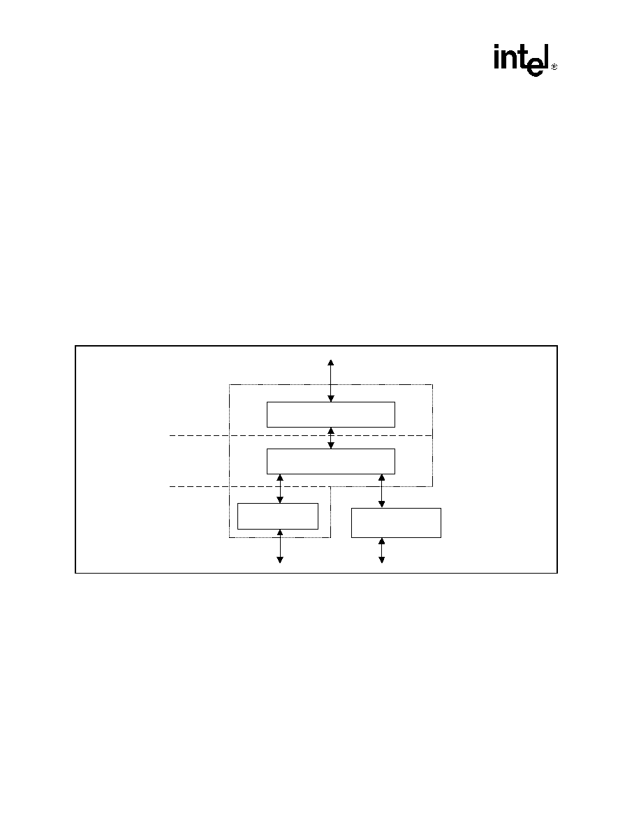
LXT970A -- Dual-Speed Fast Ethernet Transceiver
36
Datasheet
2.8.1.1
100X Preamble Handling
When the MAC asserts TX_EN, the PCS substitutes a /J/K symbol pair, also known as the Start of
Stream Delimiter or SSD, for the first two nibbles received across the MII. The PCS layer
continues to encode the remaining MII data, following
Table 17
, until TX_EN is de-asserted. It
then returns to supplying IDLE symbols to the line driver.
In the receive direction, the PCS layer performs the opposite function, substituting two preamble
nibbles for the SSD.
2.8.1.2
10T Preamble Handling
In 10BASE-T Mode, the LXT970A strips the entire preamble off of received packets. CRS is
asserted a few bit times after carrier is detected. RX_DV is held for the duration of the preamble.
When RX_DV is asserted, the very first two nibbles driven by the LXT970A are the SFD "5D" hex
followed by the body of the packet. In 10T loopback
the LXT970A loops back whatever the MAC transmits to it, including the preamble.
2.8.1.3
Data Errors (100X Only)
Figure 16
shows normal reception. When the LXT970A receives invalid symbols from the line, it
asserts RX_ER, as shown in
Figure 17
.
Figure 15. LXT970A Protocol Sublayers
Encoder/Decoder
Serializer/De-serializer
Scrambler/De-
scrambler
Link/Carrier Detect
PCS
Layer
PMA
Layer
PMD
Layer
MII Interface
PECL Interface
Fiber Transceiver
LXT970A
100BASETX
100BASE-FX
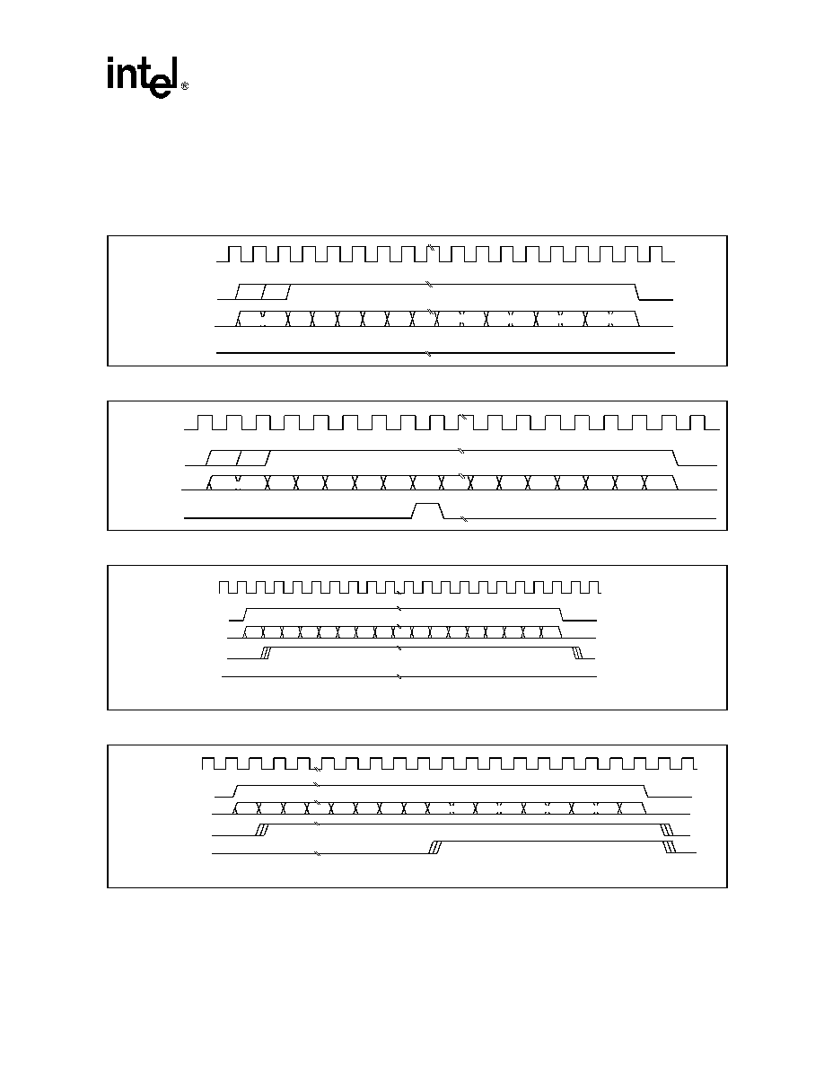
Dual-Speed Fast Ethernet Transceiver -- LXT970A
Datasheet
37
2.8.1.4
Collision Indication
Figure 18
shows normal transmission. The LXT970A detects a collision if transmit and receive are
active at the same time. As shown in
Figure 19
upon detection of a collision, the COL output is
asserted and remains asserted for the duration of the collision.
Figure 16. 100BASE-TX Reception with No Errors
Figure 17. 00BASE-TX Reception with Invalid Symbol
Figure 18. 00BASE-TX Transmission with No Errors
Figure 19. 00BASE-TX Transmission with Collision
RX_CLK
RX_DV
RXD<3:0>
RX_ER
SFD
SFD
DA
DA
DA
DA
CRC
CRC
CRC
CRC
preamble
RX_CLK
RX_DV
RXD<3:0>
RX_ER
SFD
SFD
DA
DA
DA
XX
DA
DA
DA
DA
DA
DA
DA
DA
preamble
TX_CLK
TX_EN
TXD<3:0>
CRS
COL
P
R
E
A
M
B
L
E
DA
DA
DA
DA
DA
DA
DA
DA
DA
1. In half-duplex mode, CRS asserts when receive or transmit are active. In full-duplex mode, CRS asserts during receive only.
TX_CLK
TX_EN
TXD<3:0>
CRS
COL
P
R
E
A
M
B
L
E
JAM
JAM
JAM
JAM
1. In half-duplex mode, CRS asserts when receive or transmit is active. In full-duplex mode, CRS asserts during receive only.

LXT970A -- Dual-Speed Fast Ethernet Transceiver
38
Datasheet
2.8.1.5
SQE (10T Only)
When the SQE (heartbeat) function is enabled, the LXT970A asserts its COL output for 5-15 BT
after each packet. By default, the SQE function is disabled on the LXT970A. To enable SQE, set
bit 19.10 = 1. See
Figure 30 on page 59
for SQE timing parameters.
2.8.1.6
Jabber (10T Only)
If the MAC transmission exceeds the jabber timer, the LXT970A disables the transmit and
loopback functions and asserts the COL pin. The LXT970A automatically exits jabber mode after
250-750 ms. This function can be disabled by setting bit 19.9 = 1. See
Figure 31 on page 59
for
Jabber timing parameters.
2.8.2
PMA Layer
The Physical Medium Attachment (PMA) layer provides link and carrier status functions.
2.8.2.1
100TX Link Options
The LXT970A uses standard symbol error rate criteria to establish a link and has two options for
100TX and 100FX applications to break down a link:
�
Standard (symbol error rate).
�
Enhanced (scrambler lock).
Standard link criteria (17.2 = 0 default), takes down the link when the Bit Error Rate (BER)
exceeds the allowable standards. If the link goes down and auto-negotiation is enabled, the device
automatically restarts the auto-negotiation process. Otherwise the device continues to monitor the
line for a valid link. With this option both link up and link loss are based on symbol error rate.
Enhanced link-loss criteria (17.2 = 1) works independent of symbol error rate. The loss of
scrambler lock for more than 1 - 2 msec brings the link down. Enhanced link-loss criteria is not
available in 5B mode.
2.8.2.2
10T Link Test
For 10T operation, link is detected via Normal Link Pulses (NLPs). In 10T mode, the LXT970A
always transmits link pulses. If the Link Test Function is enabled, it monitors the connection for
link pulses. Once it detects 2 to 7 link pulses, data transmission will be enabled and remains
enabled as long as the link pulses or data transmission continues. Link failure occurs if Link Test is
enabled and link pulses are no longer received. When this condition occurs, the LXT970A returns
to the auto-negotiation phase if auto-negotiation is enabled. If the Link Test function is disabled,
the LXT970A transmits to the connection regardless of detected link pulses. The Link Test
function can be disabled by setting bit 19.8 = 1 or by setting MF0 to disable auto-negotiation and
setting CFG1 input High.
2.8.2.3
Carrier Sense (CRS)
For 100TX and 100FX links, a start-of-stream delimiter or /J/K symbol pair causes assertion of
carrier sense (CRS). An end-of-stream delimiter, or /T/R symbol pair causes deassertion of CRS.
The PMA layer also de-asserts CRS if IDLE symbols are received without /T/R, however, in this
case RX_ER asserts for one clock cycle when CRS is de-asserted.

Dual-Speed Fast Ethernet Transceiver -- LXT970A
Datasheet
39
For 10T links, CRS assertion is based on reception of valid preamble, and de-assertion on reception
of an end-of-frame (EOF) marker.
The PMA layer in the LXT970A does not support the optional Far-End-Fault function.
2.8.3
Twisted-Pair PMD Layer
The twisted-pair Physical Medium Dependent (PMD) layer provides the signal scrambling and
descrambling, line coding and decoding (MLT-3 for 100TX, Manchester for 10T), as well as
receiving, polarity correction, and baseline wander correction functions.
2.8.3.1
Scrambler/Descrambler (100TX Only)
The scrambler spreads the signal power spectrum and reduces EMI and baseline wander.
Scrambling is done with an 11-bit, non-data-dependent polynomial. The receiver automatically
decodes the polynomial whenever IDLE symbols are received.
The LXT970A provides a scrambler-bypass mode for testing purposes. Bypassing the scrambler
causes the PCS-layer encoder to be bypassed as well, and the MII to operate in 5B mode.
2.8.3.2
Baseline Wander Correction
(100TX Only)
The LXT970A provides a baseline wander correction function that makes the device robust under
all network operating conditions. The MLT3 coding scheme used in 100BASE-TX is by definition
"unbalanced", which means the average DC value of the signal voltage can "wander" significantly
over short time intervals (tenths of seconds). In less robust PHY devices, this wander can cause
receiver errors, particularly at long line lengths (100 meters). The exact characteristics of the
wander are completely data dependent. The LXT970A baseline wander correction circuitry allows
error-free data recovery, even at long line lengths.
2.8.3.3
Polarity Correction
The LXT970A automatically detects and corrects for the condition where the receive signal (TPIP/
N) is inverted. Reversed polarity is detected if eight inverted link pulses, or four inverted end-of-
frame markers, are received consecutively. If link pulses or data are not received for 96-128 ms,
the polarity state is reset to a non-inverted state.
2.8.4
Fiber PMD Layer
The LXT970A provides a pseudo-ECL interface for connection to an external fiber optic
transceiver. (The external transceiver provides the PMD function for fiber media.) The LXT970A
uses an NRZI format for the fiber interface. The fiber interface operates at 100 Mbps and is
intended for 100FX applications. It does not support 10FL applications. The fiber interface does
not support the signal detect function supplied by most fiber optic transceivers. However, the link
detection function in the PMA layer quickly detects faults in the fiber link.

LXT970A -- Dual-Speed Fast Ethernet Transceiver
40
Datasheet
2.8.5
Additional Operating Features
2.8.6
Low-Voltage-Fault Detect
The LXT970A low-voltage fault detection function prevents transmission of invalid symbols when
VCC goes below normal operating levels. If this condition occurs, the LXT970A disables the
transmit outputs and sets 20.2 = 1. Operation is automatically restored when V
CC
returns to
normal.
Table 26 on page 49
indicates voltage levels that detect and clear the low-voltage fault
condition.
2.8.7
Power Down Mode
The LXT970A goes into power down mode when PWRDWN is asserted. In this mode, all
functions are disabled except the MDIO. The power supply current is significantly reduced. This
mode can be used for energy-efficient applications or for redundant applications where there are
two devices and one is left as a stand-by. When the LXT970A is returned to normal operation,
configuration settings of the MDIO registers are maintained. Refer to
Table 22 on page 47
for
power down specifications.
2.8.8
Software Reset
Software reset causes all state machines to be reset and the LXT970A to re-configure itself to the
settings of the hardware configuration pins (MF<4:0>, FDE, CFG0, CFG1).
The LXT970A is reset via software(0.15 = 1). This bit setting is maintained while the reset
operation is running. When the reset operation is complete, the LXT70 resets bit 0.15 = 0.
2.8.9
Hardware Reset
Hardware reset causes the LXT970A to reset all of its functions and re-configure itself based on the
hardware configuration pin settings.
The LXT970A performs a hardware reset when a Low signal is detected at the RESET pin. All
operational conditions must be met for this function to operate. V
CC
must be above 4.75V and
stable, and the RESET signal must be asserted for two cycles of the master input clock. The
LXT970A continues to drive an internal reset for a period of 300
�
s after the RESET signal is de-
asserted to ensure that all functions start up smoothly. MII registers are not available and the MDIO
output is tri-stated during the internal reset period. Refer to
Table 43 on page 62
for hardware reset
specifications.
Dual-Speed Fast Ethernet Transceiver -- LXT970A
Datasheet
41
3.0
Application Information
3.1
Magnetics Information
The LXT970A requires a 1:1 ratio for both the receive and the transmit transformers. Refer to
Table 18
for magnetics requirements.
A cross-reference list of magnetic manufacturers and part numbers is available in Application Note
73, Magnetic Manufacturers, which can be found on the Intel web site (developer.intel.com/design/
network/). Designers must test and evaluate all components for suitability in their applications.
3.2
Crystal Information
The LXT970A requires a parallel-resonant fundamental-mode crystal that meet specifications as
shown in
Table 19
. XI and XO input capacitance and voltage requirements are provided in
Table 25
on page 48
.
Crystals are available from various manufacturers. Designers should test and validate all crystals
before committing to a specific component. Based on limited evaluation,
Table 20
provides
suitable crystal component manufacturers.
Table 18. Magnetics Requirements
Parameter
Min
Nom
Max
Units
Test Condition
Rx and Tx Turns Ratio
�
1:1
�
�
Insertion Loss
0.0
�
1.1
dB
Primary Inductance
350
�
�
�
H
Transformer Isolation
�
2
�
kV
Differential to common mode rejection
�
�
-40
dB
.1 to 60 MHz
�
�
-35
dB
60 to 100 MHz
Return Loss
�
�
-17
dB
.1 to 60 MHz
�
�
-15
dB
60 to 100 MHz
Rise Time
2.0
�
3.5
ns
10% to 90%
Table 19. Crystal Requirements
Parameter
Min
Nom
Max
Units
Test Condition
Frequency
�
25.0
�
MHz
Frequency Stability
�
�
�100
ppm
-40 - 85
o
C
1. See
Table 25
(Clock Characteristics) for additional device specifications.
Table 20. Crystal Component Manufacturers
Component
Manufacturer
Part Number
Crystal
Epson America
MA-505-25.000M
Caliber Electronics
AA18C1-25.000MHz

LXT970A -- Dual-Speed Fast Ethernet Transceiver
42
Datasheet
3.3
Design Recommendations
The LXT970A is designed in accordance with IEEE requirements and provides outstanding
receive Bit Error Ratio (BER) and long-line-length performance. Lab tests show that the
LXT970A performs well beyond the required distance of 100 meters. Ensuring maximum
performance from the LXT970A requires attention to detail and good design practices. Refer to
the LXT970 Design and Layout Guide for detailed design and layout information.
3.3.1
General Design Guidelines
Adherence to generally accepted design practices is essential to minimize noise levels on power
and ground planes. Up to 50 mV of noise is considered acceptable. 50 to 80 mV of noise is
considered marginal. High-frequency switching noise can be reduced, and its effects can be
eliminated, by following these simple guidelines throughout the design:
�
Fill in unused areas of the signal planes with solid copper and attach them with vias to a VCC
or ground plane that is not located adjacent to the signal layer.
�
Use ample bulk and decoupling capacitors throughout the design (a value of .01
�
F is
recommended for decoupling caps).
�
Provide ample power and ground planes.
�
Provide termination on all high-speed switching signals and clock lines.
�
Provide impedance matching on long traces to prevent reflections.
�
Route high-speed signals next to a continuous, unbroken ground plane.
�
Filter and shield DC-DC converters, oscillators, etc.
�
Do not route any digital signals between the LXT970A and the RJ-45 connectors at the edge of
the board.
�
Do not extend any circuit power and ground plane past the center of the magnetics or to the
edge of the board. Use this area for chassis ground, or leave it void.
3.3.2
Power Supply Filtering
Power supply ripple and digital switching noise on the VCC plane can cause EMI problems and
degrade line performance. It is generally difficult to predict in advance the performance of any
design, although certain factors greatly increase the risk of having these problems:
�
Poorly-regulated or over-burdened power supplies.
�
Wide data busses (>32-bits) running at a high clock rate.
�
DC-to-DC converters.
Many of these issues can be improved by following good general design guidelines. Intel also
recommends filtering between the power supply and the analog VCC pins of the LXT970A.
Filtering has two benefits. First, it keeps digital switching noise out of the analog circuitry inside
the LXT970A, which helps line performance. Second, if the VCC planes are laid out correctly, it
keeps digital switching noise away from external connectors, reducing EMI problems.

Dual-Speed Fast Ethernet Transceiver -- LXT970A
Datasheet
43
The recommended implementation is to divide the VCC plane into two sections. The digital
section supplies power to the digital VCC pin, VCCIO pin, and to the external components. The
analog section supplies power to VCCA, VCCT, and VCCR pins of the LXT970A. The break
between the two planes should run under the device. In designs with more than one LXT970A, a
single continuous analog VCC plane can be used to supply them all.
The digital and analog VCC planes should be joined at one or more points by ferrite beads. The
beads should produce at least a 100
impedance at 100 MHz. The beads should be placed so that
current flow is evenly distributed. The maximum current rating of the beads should be at least
150% of the current that is actually expected to flow through them. A bulk cap (2.2 -10
�
F) should
be placed on each side of each ferrite bead to stop switching noise from traveling through the
ferrite.
In addition, a high-frequency bypass cap (.01
�
f) should be placed near each analog VCC pin.
3.3.3
Ground Noise
The best approach to minimize ground noise is strict use of good general design guidelines and by
filtering the VCC plane.
3.3.4
Power and Ground Plane Layout Considerations
Great care needs to be taken when laying out the power and ground planes. The following
guidelines are recommended:
�
Follow the guidelines in the LXT970 Layout Guide for locating the split between the digital
and analog VCC planes.
�
Keep the digital VCC plane away from the TPOP/N and TPIP/N signals, away from the
magnetics, and away from the RJ-45 connectors.
�
The ground plane should be one continuous, unbroken plane.
�
Place the layers so that the TPOP/N and TPIP/N signals can be routed near or next to the
ground plane. It is more important to shield TPOP/N than TPIP/N for EMI reasons.
3.3.5
Interfaces for Twisted-Pair /Fiber
3.3.5.1
Twisted-Pair
Figure 21 on page 46
shows the recommended termination circuits for the fiber and twisted-pair
interfaces. The twisted-pair interface consists of magnetics and a 100
termination resistance in
parallel on the device-side of the winding. On the transmit pair, a common-mode bypass capacitor
to ground is strongly recommended. A similar technique on the receive side can improve
performance in some cases, however the results are highly application specific and must be
verified. Route TREF nearby, but not in-between TPOP and TPON. A "Bob Smith" termination is
often provided for the unused signal pairs.

LXT970A -- Dual-Speed Fast Ethernet Transceiver
44
Datasheet
3.3.5.2
Fiber
The fiber interface consists of a pseudo-ECL transmit and receive pair to an external fiber optic
transceiver. The transmit pair should be AC-coupled to the transceiver, and biased to 3.7V with a
50
equivalent impedance. The receive pair can be DC-coupled, and should be biased to 3.0V with
a 50
equivalent impedance.
Figure 21 on page 46
shows the correct bias networks to achieve
these requirements.
The following guidelines apply to when laying out any differential pair:
�
Space both members close together allowing nothing to come between them.
�
Keep distances as short as possible, both traces should have the same length.
�
Avoid layer changes as much as possible.
�
Keep termination circuits close together and on the same side of the board.
�
Always put termination circuits close to the source end of any circuit.
3.3.6
Interface for the MII
3.3.6.1
Transmit Hold Time Adjustment
Transmit hold time for TXD, TX_EN, and TX_ER from TX_CLK High is currently specified in
Table 32
,
Table 34
,
Table 36
, and
Table 38
as 5 ns minimum. 0 ns minimum is the IEEE
specification. Depending on the specification of the MAC or ASIC used in your design, you may or
may not need to account for this in your PC board design.
If you determine that a timing adjustment is required, there are a couple of recommended ways to
do this.
�
If using series resistors in the TXD lines, increase the value of the resistors to achieve the
necessary delay.
�
An alternative method is to add the appropriate delay in the TX_CLK line. Depending on the
amount of delay required, this may be accomplished with a series resistor or by adding a buffer
to the TX_CLK line.
Note that some delay is introduced by the actual PC board traces themselves.
3.3.6.2
MII Terminations
When the LXT970A is configured with high-strength MII driver levels (bit 17.3 = 0), 55
series
termination resistors are recommended on all MII output signals to avoid undershoot and
overshoot.
When 17.3 = 1, the MI driver levels are reduced by a factor of ten and termination resistors are not
required on the MII outputs.
Dual-Speed Fast Ethernet Transceiver -- LXT970A
Datasheet
45
3.3.7
Typical Application
Figure 21 on page 46
is typical interface circuitry of the LXT970A. The diagram groups similar
pins; it does not portray the actual chip pinout. The Media Independent Interface (MII) pins are at
the upper left. Hardware Control Interface pins are center left. The line interface pins for twisted-
pair and fiber are shown on the top and bottom right respectively.
The VCCD and VCCIO pins are at the bottom of the diagram. VCCT, VCCR, and VCCA are at the
center right. All VCC pins (except VCCIO) use a single power supply. VCCIO may be powered by
a 3.3V supply, and may be separately connected.
3.3.7.1
Voltage Divider For MF Inputs
The LXT970A requires an external voltage divider to provide optional (V
MF
2 and V
MF
3) multi-
level inputs to the Multi-Function (MF) pins. These voltage levels are designated as V
MF
1 - V
MF
4.
A single voltage divider may be used to drive the MF pins in designs using multiple PHYs.
Figure
20
shows a voltage divider with three 1 k
resistors configured in series between VCC and
Ground.
Figure 20. Voltage Divider
V
MF
4
V
MF
3
V
MF
2
+5V
V
MF
1
1k
W
1k
W
1k
W
LXT970A -- Dual-Speed Fast Ethernet Transceiver
46
Datasheet
Figure 21. Typical Interface Circuitry
LXT970A
25.0 MHz
C1
C2
XI
TX_EN
TPIN
TPIP
RJ45
T
o
T
w
isted-P
a
ir Network
RBIAS
GNDD
TXD<4:0>
TX_CLK
TX_ER
COL
RX_DV
RX_ER
RX_CLK
RXD<4:0>
CRS
MDIO
FDS/MDINT
MDC
MII
Data
I/F
+5 V
VCCD
XO
TPON
50
1%
TPOP
50
1%
50
50
50
75
50
50
TREF
VCCIO
+3.3V
or
+5V
GNDIO
50
6
5
4
3
2
1
8
7
VCCT
GNDT
FIBON
191
W
FIBOP
FIBIN
FIBIP
191
W
69
W
69
W
Fiber Txcvr
T
o
F
i
ber N
e
tw
ork
.01
m
F
130
W
130
W
80
W
80
W
+5 V
.01
m
F
TD
TD
RD
RD
3
2
1
VCCA
GNDA
TEST
LEDS
LEDR
LEDT
LEDL
LEDC
330
W
330
W
330
W
330
W
330
W
+5 V
75
VCCR
GNDR
.01
�
F
.01
�
F
MF<4:0>
CFG<1:0>
RESET
PWRDWN
H/W
Control
I/F
FDE
TRSTE
MDDIS
MII
Control
I/F
.01
�
F
.01
�
F
0.001
�
F/2kV
.01
�
F
.01
�
F
22.1k
1%
.01
�
F
.01
m
F
10
�
F
GNDD
GNDD
GNDA
GNDA
GNDA
GNDA
VCCR
GNDD
VCCD
Ferrite Bead
+5 V
10
�
F
VCCA
GNDA
10
�
F
+
+
4
VCCT
+5 V
+
.01
m
F
50
1%
50
1%
.01
�
F
GNDR
5
6
7
55
55
55
55
55
55
55
1. Refer to
Table 19
and
Table 20
for crystals.
2. Refer to
Table 18
for magnetics.
3. Refer to fiber transceiver manufacturers recommendations for termination circuitry. Suitable fiber transceivers include:
HFBR-5103 and HFBR-5105.
4. Bypassing to chassis ground (if available) provides additional EMI shielding.
5. If the fiber interface is not used, FIBIN, FIBIP, FIBON, and FIBOP may be left unconnected.
6. Placement of this cap should be verified for each application. This cap typically reduces error rates at long line lengths but
is implementation specific.
7. If bit 17.3 = 0, series terminations resistors are recommended for all MII outputs. The proper value is application specific.
If bit 17.3 = 1, termination resistors are not required.
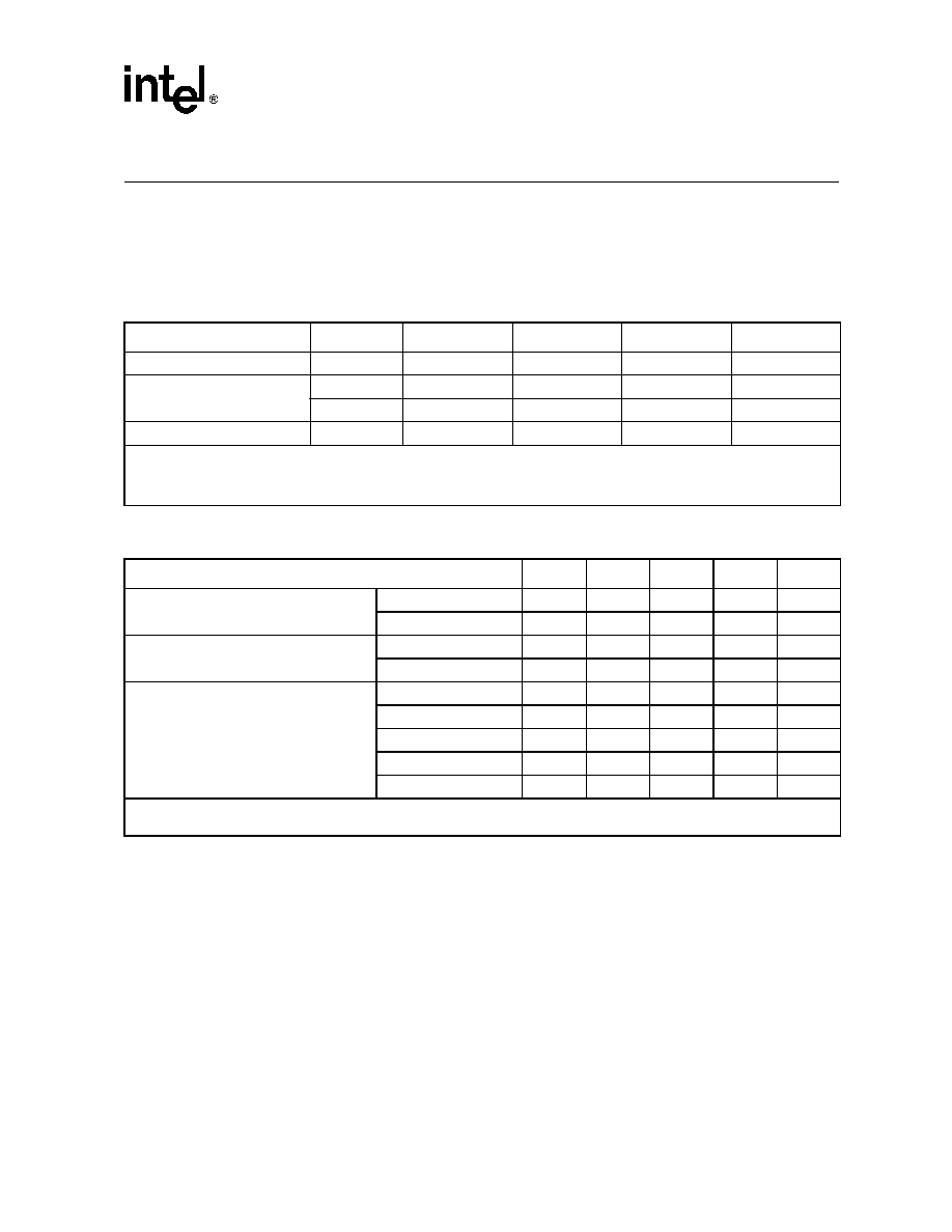
Dual-Speed Fast Ethernet Transceiver -- LXT970A
Datasheet
47
4.0
Test Specifications
Note:
Table 21
through
Table 43
and
Figure 22
through
Figure 36
represent the performance
specifications of the LXT970A. These specifications are guaranteed by test except where noted "by
design." Minimum and maximum values listed in
Table 23
through
Table 43
apply over the
recommended operating conditions specified in
Table 22
.
Table 21. Absolute Maximum Ratings
Parameter
Sym
Min
Max
Units
Supply Voltage
V
CC
-0.3
6
V
Operating Temperature
Ambient
T
OPA
-15
+85
�C
Case
T
OPC
�
+120
�C
Storage Temperature
T
ST
-65
+150
�C
Caution:
Exceeding these values may cause permanent damage. Functional operation under these
conditions is not implied. Exposure to maximum rating conditions for extended periods may
affect device reliability.
Table 22. Operating Conditions
Parameter
Sym
Min
Typ
1
Max
Units
Recommended Supply Voltage
2
Except MII Supply
V
CC
4.75
5.0
5.25
V
MII Supply
V
CCIO
3.125
�
5.25
V
Recommended Operating Temperature
Ambient
T
OPA
0
�
70
�C
Case
T
OPC
0
�
110
�C
Power Consumption
(+5V Only)
100BASE-TX
I
CC
�
170
�
mA
100BASE-FX
I
CC
�
80
�
mA
10BASE-T
I
CC
�
185
�
mA
Power-Down Mode
I
CC
�
9
�
mA
Auto-Negotiation
I
CC
�
240
270
mA
1. Typical values are at 25 �C and are for design aid only; not guaranteed and not subject to production testing.
2. Voltages with respect to ground unless otherwise specified.
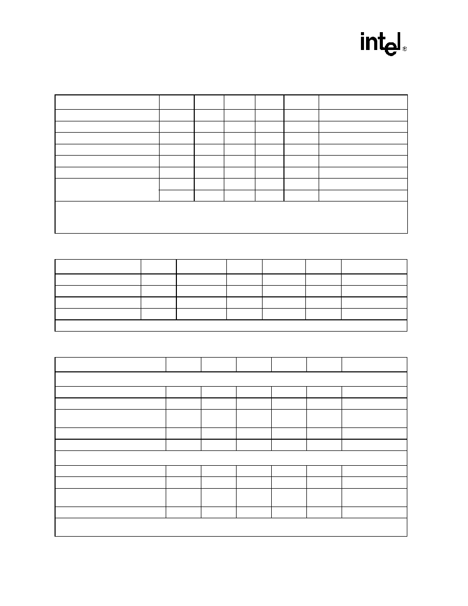
LXT970A -- Dual-Speed Fast Ethernet Transceiver
48
Datasheet
Table 23. Digital I/O Characteristics
1
Parameter
Symbol
Min
Typ
Max
Units
Test Conditions
Input Low Voltage
3
V
IL
�
�
.8
V
Input High Voltage
3
V
IH
2.0
�
�
V
Input Current
I
I
-10
�
10
�
A
0.0 < V
I
< V
CC
Output Low Voltage
V
OL
�
�
0.4
V
I
OL
= 4 mA
Output High Voltage (MII only)
V
OH
2.2
�
�
V
I
OH
= -4 mA, V
CCIO
=3.3V
Output High Voltage
V
OH
2.4
�
�
V
I
OH
= -4 mA, V
CCIO
=5.0V
MII Driver Output Resistance
(Line Driver Output Enabled)
R
O
2,4
6.0
�
25.0
V
CCIO
= 3.3V
R
O
2,4
6.0
�
25.0
V
CCIO
= 5.0V
1. Applies to all pins except MF<4:0> pins. Refer to
Table 24
for MF pin I/O Characteristics.
2. Parameter is guaranteed by design and not subject to production testing.
3. Does not apply to XI or TX_CLK pins. Refer to
Table 25
for clock input levels.
4. Applies to default MII driver level (bit 17.3= 0).
Table 24. Digital I/O Characteristics - MultiFunction Pins MF<4:0>
Parameter
Symbol
Min
Typ
1
Max
Units
Test Conditions
Input Voltage Level 1
V
MF
1
V
CC
- 0.5
�
�
V
Input Voltage Level 2
V
MF
2
(V
CC
/2) + 0.5
�
V
CC
- 1.2
V
Input Voltage Level 3
V
MF
3
1.2
�
V
CC
/2 - 0.5
V
Input Voltage Level 4
V
MF
4
�
�
0.5
V
1. Typical values are at 25 �C and are for design aid only; not guaranteed and not subject to production testing.
Table 25. Required Clock Characteristics
Parameter
Sym
Min
Typ
1
Max
Units
Test Conditions
Master Clock Mode - External XI Clock Input
Input Low Voltage
2
V
IL
�
�
1.0
V
Input High Voltage
2
V
IH
3.2
�
�
V
Input Clock Frequency Tolerance
2
f
�
�
� 100
ppm
Clock frequency is 25
MHz or 2.5 MHz
Input Clock Duty Cycle
2
Tdc
40
�
60
%
Input Capacitance (XI and XO)
C
IN
�
3.0
�
pF
Slave Clock Mode - External TX_CLK Input
Input Low Voltage
V
IL
�
�
.8
V
Input High Voltage
V
IH
2.0
�
�
V
Input Clock Frequency Tolerance
2
f
�
�
� 100
ppm
Clock frequency is 25
MHz or 2.5 MHz
Input Clock Duty Cycle
2
Tdc
35
�
65
%
1. Typical values are at 25 �C and are for design aid only; not guaranteed and not subject to production testing.
2. Parameter is guaranteed by design; not subject to production testing.
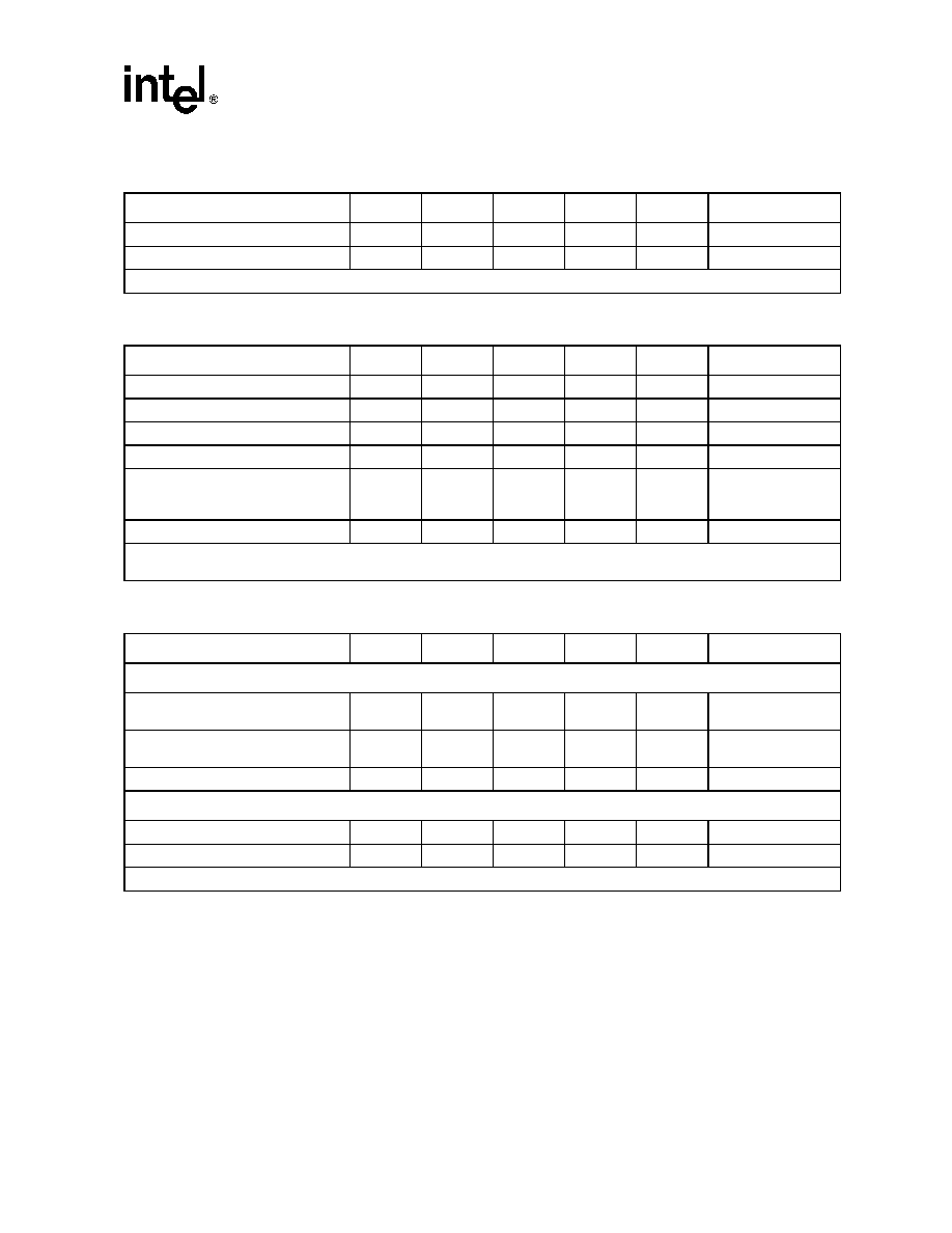
Dual-Speed Fast Ethernet Transceiver -- LXT970A
Datasheet
49
Table 26. Low Voltage Fault Detect Characteristics
Parameter
Sym
Min
Typ
1
Max
Units
Test Conditions
Detect Fault Threshold
V
LT
3.4
�
4.0
V
�
Clear Fault Threshold
V
LH
4.1
�
4.7
V
�
1. Typical values are at 25 �C and are for design aid only; not guaranteed and not subject to production testing.
Table 27. 100BASE-TX Transceiver Characteristics
Parameter
Sym
Min
Typ
1
Max
Units
Test Conditions
Peak Differential Output Voltage
V
OP
0.95
�
1.05
V
Note 2
Signal Amplitude Symmetry
Vss
98
�
102
%
Note 2
Signal Rise/Fall Time
T
RF
3.0
�
5.0
ns
Note 2
Rise/Fall Time Symmetry
T
RFS
�
�
0.5
ns
Note 2
Duty Cycle Distortion
D
CD
�
�
� 0.5
ns
Offset from 16ns
pulse width at 50% of
pulse peak
Overshoot/Undershoot
V
OS
�
�
5
%
�
1. Typical values are at 25 �C and are for design aid only; not guaranteed and not subject to production testing.
2. Measured at the line side of the transformer, line replaced by 100
(�1%) resistor.
Table 28. 100BASE-FX Transceiver Characteristics
Parameter
Sym
Min
Typ
1
Max
Units
Test Conditions
Transmitter
Peak Differential Output Voltage
(Single Ended)
V
OP
0.6
�
1.0
V
�
Signal Rise/Fall Time
T
RF
�
�
1.6
ns
10 <�> 90%
2.0 pF load
Jitter (Measured Differentially)
�
�
�
1.3
ns
�
Receiver
Peak Differential Input Voltage
V
IP
0.55
�
1.5
V
�
Common-Mode Input Range
V
CMIR
2.25
�
VCC - 0.5
V
�
1. Typical values are at 25 �C and are for design aid only; not guaranteed and not subject to production testing.
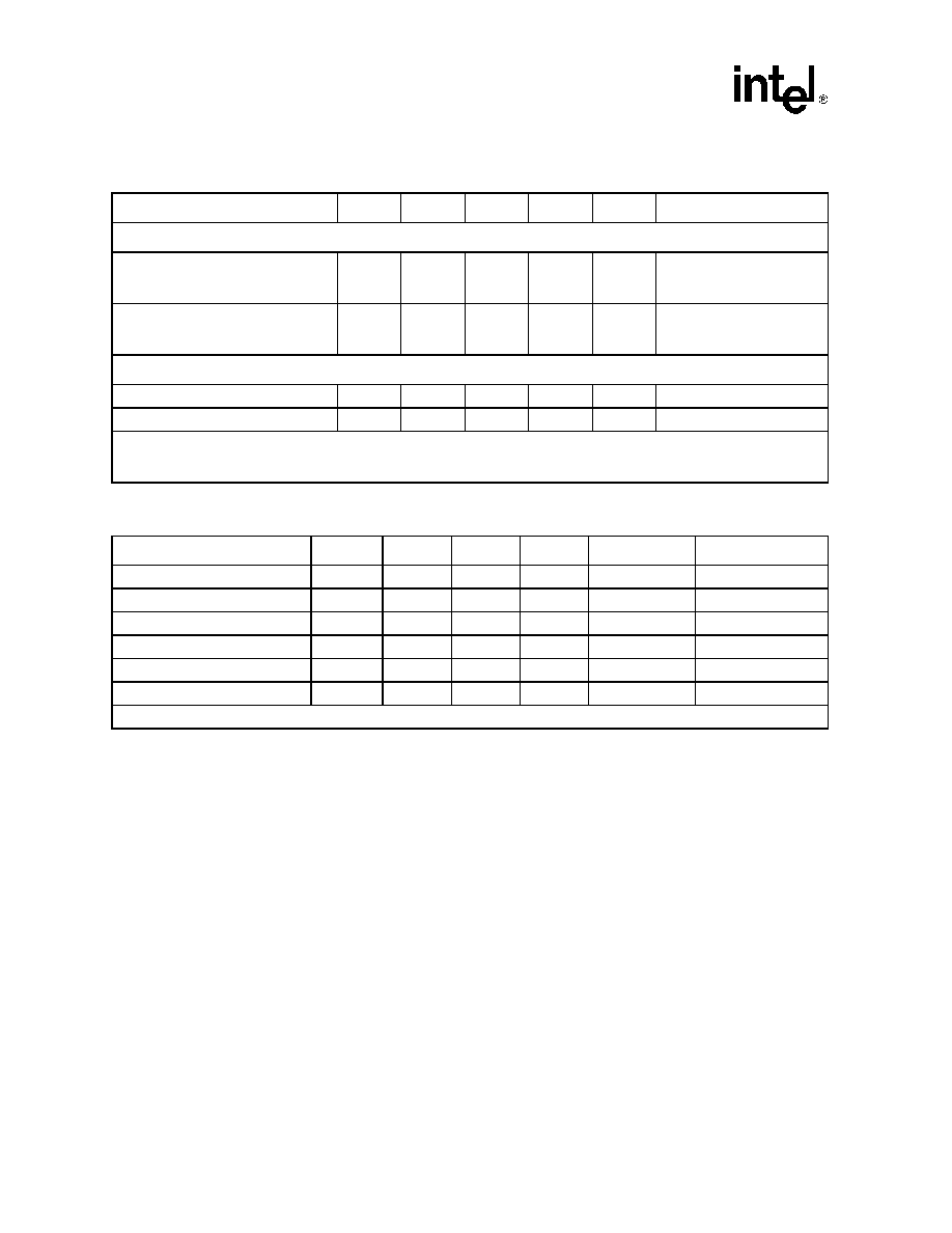
LXT970A -- Dual-Speed Fast Ethernet Transceiver
50
Datasheet
Table 29. 10BASE-T Transceiver Characteristics
Parameter
Sym
Min
Typ
1
Max
Units
Test Conditions
Transmitter
Peak Differential
Output Voltage
V
OP
2.2
2.5
2.8
V
With transformer, line
replaced by 100
(�1%)
resistor
Transmit Timing Jitter added by the
MAU and PLS Sections
2,3
�
0
2
11
ns
After line model specified by
IEEE 802.3 for 10BASE-T
MAU
Receiver
Receive Input Impedance
2
Z
IN
�
3.6
�
k
Between TPIP/TPIN
Differential Squelch Threshold
V
DS
300
420
585
mV
5 MHz square wave input
1. Typical values are at 25 �C and are for design aid only; not guaranteed and not subject to production testing.
2. Parameter is guaranteed by design; not subject to production testing.
3. IEEE 802.3 specifies maximum jitter additions at 1.5 ns for the AUI cable, 0.5ns from the encoder, and 3.5ns from the MAU.
Table 30. 10BASE-T Link Integrity Timing Characteristics
Parameter
Sym
Min
Typ
1
Max
Units
Test Conditions
Time Link Loss Receive
T
LL
50
64
150
ms
�
Link Pulse
T
LP
2
4
7
Link Pulses
�
Link Min Receive Timer
T
LR
M
IN
2
4
7
ms
�
Link Max Receive Timer
T
LR
M
AX
50
64
150
ms
�
Link Transmit Period
Tlt
8
10
24
ms
�
Link Pulse Width
Tlpw
�
100
�
ns
�
1. Typical values are at 25 �C and are for design aid only; not guaranteed and not subject to production testing.
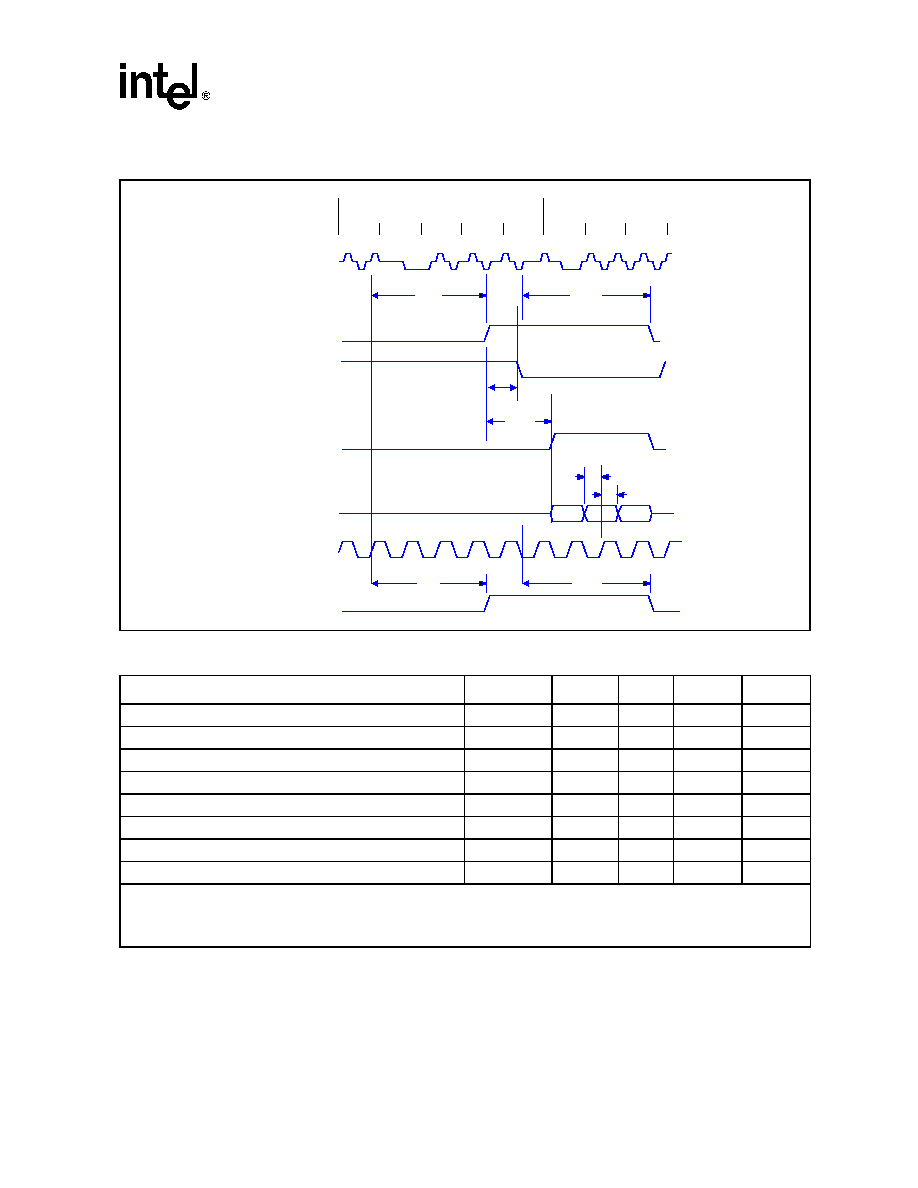
Dual-Speed Fast Ethernet Transceiver -- LXT970A
Datasheet
51
Figure 22. MII - 100BASE-TX Receive Timing / 4B Mode
Table 31. MII - 100BASE-TX Receive Timing Parameters / 4B Mode
Parameter
Sym
Min
Typ
1
Max
Units
3
RXD, RX_DV, RX_ER Setup to RX_CLK High
t1A
10
�
�
ns
RXD, RX_DV, RX_ER Hold from RX_CLK High
t1B
10
�
�
ns
CRS asserted to RXD<3:0>, RX_DV asserted
t1C
�
8
�
BT
Receive start of "J" to CRS asserted
t1D
0
15 - 19
20
BT
Receive start of "T" to CRS de-asserted
t1E
13
23 - 27
28
BT
Receive start of "J" to COL asserted
t1F
0
15 - 19
20
BT
Receive start of "T" to COL de-asserted
t1G
13
23 - 27
28
BT
TRSTE asserted to RX_DV, RXD<3:0> driven
2
t1H
�
20
�
ns
1. Typical values are at 25 �C and are for design aid only; not guaranteed and not subject to production testing.
2. These parameters apply only when the device is operated in Repeater Mode.
3. BT is the duration of one bit as transferred to and from the MAC and is the reciprocal of the bit rate. 100BASE-T bit time = 10
-
8
s or 10 ns.
t1D
t1E
t1C
t1F
t1G
0ns
250ns
CRS
TRSTE
1
RX_DV
RXD<3:0>
RX_CLK
COL
t1A
t1B
TPIP
t1H
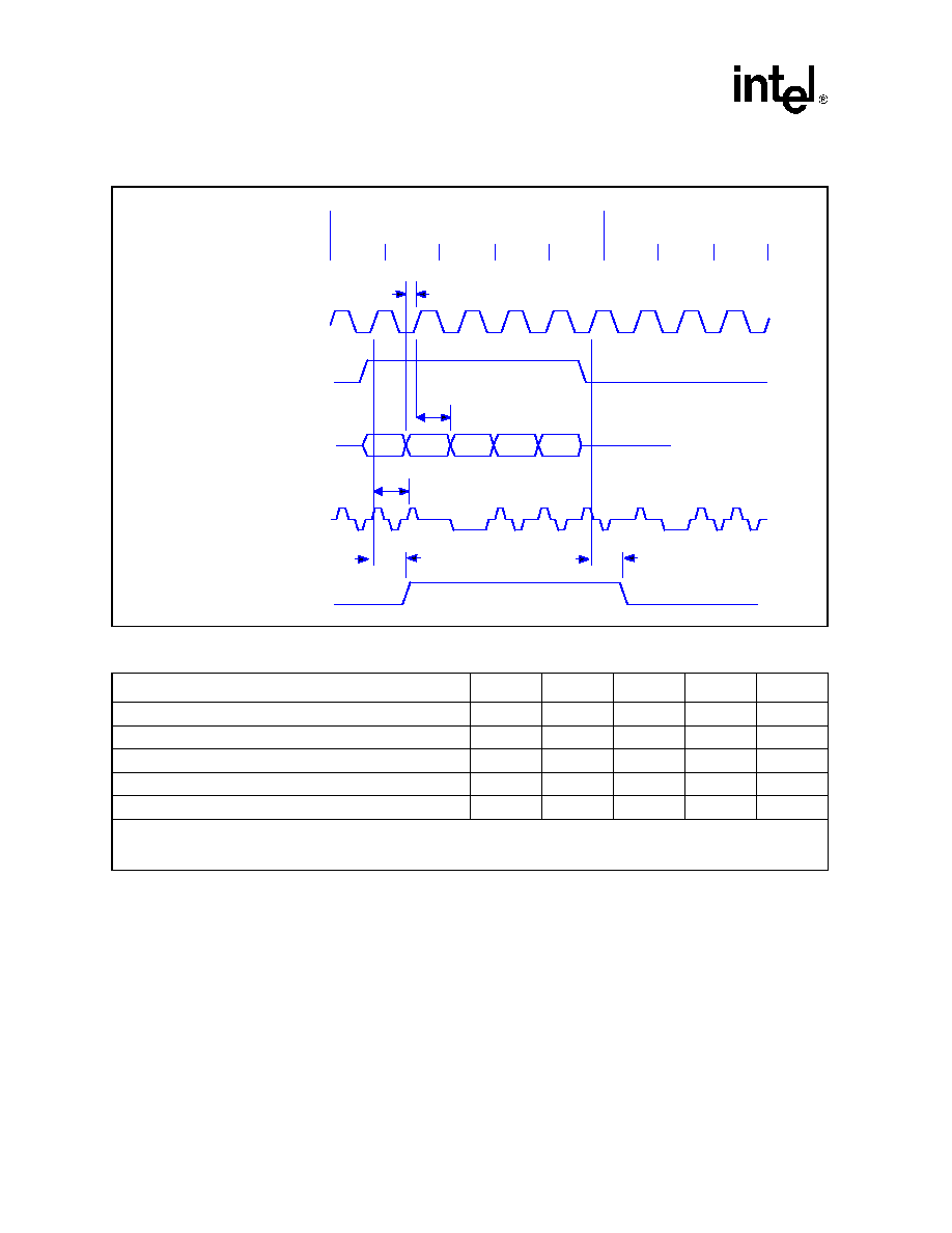
LXT970A -- Dual-Speed Fast Ethernet Transceiver
52
Datasheet
Figure 23. MII - 100BASE-TX Transmit Timing / 4B Mode
Table 32. MII - 100BASE-TX Transmit Timing Parameters / 4B Mode
Parameter
Sym
Min
Typ
1
Max
Units
2
TXD<3:0>, TX_EN, TX_ER Setup to TX_CLK High
t2A
10
�
�
ns
TXD<3:0>, TX_EN, TX_ER Hold from TX_CLK High
t2B
5
�
�
ns
TX_EN sampled to CRS asserted
t2C
�
3
4
BT
TX_EN sampled to CRS de-asserted
t2D
�
4
16
BT
TX_EN sampled to TPO out (Tx latency)
t2E
6
10
14
BT
1. Typical values are at 25 �C and are for design aid only; not guaranteed and not subject to production testing.
2. BT is the duration of one bit as transferred to and from the MAC and is the reciprocal of the bit rate. 100BASE-T bit time = 10
-
8
s or 10 ns.
t2A
t2B
t2E
t2C
t2D
0ns
250ns
TXCLK
TX_EN
TXD<3:0>
CRS
TPOP
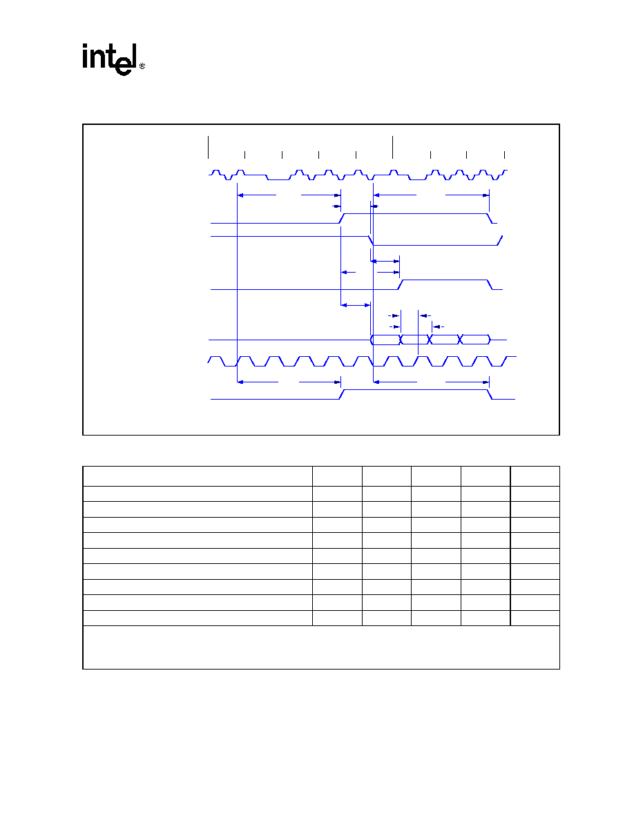
Dual-Speed Fast Ethernet Transceiver -- LXT970A
Datasheet
53
Figure 24. MII - 100BASE-TX Receive Timing / 5B Mode
Table 33. MII - 100BASE-TX Receive Timing Parameters / 5B Mode
Parameter
Sym
Min
Typ
1
Max
Units
3
RXD, RX_DV, RX_ER Setup to RX_CLK High
t3A
10
�
�
ns
RXD, RX_DV, RX_ER Hold from RX_CLK High
t3B
10
�
�
ns
CRS asserted to RX_DV asserted
t3C
�
8
�
BT
CRS asserted to RXD<4:0> asserted
t3D
�
4
�
BT
Receive start of "J" to CRS asserted
t3E
0
15 - 19
20
BT
Receive start of "T" to CRS de-asserted
t3F
13
23 - 27
28
BT
Receive start of "J" to COL asserted
t3G
0
15 - 19
20
BT
Receive start of "T" to COL de-asserted
t3H
13
23 - 27
28
BT
TRSTE asserted to RX_DV, RXD<4:0> driven
2
t3I
�
20
�
ns
1. Typical values are at 25 �C and are for design aid only; not guaranteed and not subject to production testing.
2. These parameters apply only when the device is operated in Repeater Mode.
3. BT is the duration of one bit as transferred to and from the MAC and is the reciprocal of the bit rate. 100BASE-T bit time = 10
-
8
s or 10 ns.
Note
2
t3E
t3F
t3C
t3I
1
t3D
t3G
t3H
0ns
250ns
TPIP
CRS
TRSTE
1
RX_DV
RXD<4:0>
RX_CLK
COL
t3A
t3B
1. This parameter applies only when the device is operated in Repeater Mode.
2. In Repeater Mode, application circuit must assert TRSTE within time period specified by t4 - t10.
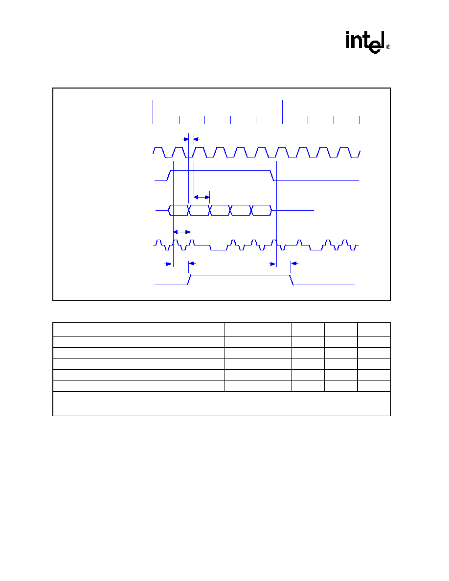
LXT970A -- Dual-Speed Fast Ethernet Transceiver
54
Datasheet
Figure 25. 100BASE-TX Transmit Timing / 5B Mode
Table 34. MII - 100BASE-TX Transmit Timing Parameters / 5B Mode
Parameter
Sym
Min
Typ
1
Max
Units
2
TXD, TX_EN, TX_ER Setup to TX_CLK High
t4A
10
�
�
ns
TXD, TX_EN, TX_ER Hold from TX_CLK High
t4B
5
�
�
ns
TX_EN sampled to CRS asserted
t4C
�
3
4
BT
TX_EN sampled to CRS de-asserted
t4D
�
4
16
BT
TX_EN sampled to TPO out (Tx latency)
t4E
4
6
9
BT
1. Typical values are at 25 �C and are for design aid only; not guaranteed and not subject to production testing.
2. BT is the duration of one bit as transferred to and from the MAC and is the reciprocal of the bit rate. 100BASE-T bit time = 10
-
8
s or 10 ns.
t4A
t4B
t4E
t4C
t4D
0ns
250ns
TXCLK
TX_EN
TXD<3:0>
CRS
TPOP
Dual-Speed Fast Ethernet Transceiver -- LXT970A
Datasheet
55
Figure 26. MII - 100BASE-FX Receive Timing / 4B Mode
Table 35. MII - 100BASE-FX Receive Timing Parameters / 4B Mode
Parameter
Sym
Min
Typ
1
Max
Units
3
RXD, RX_DV, RX_ER Setup to RX_CLK High
t5A
10
�
�
ns
RXD, RX_DV, RX_ER Hold from RX_CLK High
t5B
10
�
�
ns
CRS asserted to RXD<3:0>, RX_DV asserted
t5C
�
8
�
BT
Receive start of "J" to CRS asserted
t5D
0
13 - 17
20
BT
Receive start of "T" to CRS de-asserted
t5E
13
21 - 25
26
BT
Receive start of "J" to COL asserted
t5F
0
13 - 17
20
BT
Receive start of "T" to COL de-asserted
t5G
13
21 - 25
26
BT
TRSTE asserted to RX_DV, RXD<3:0> driven
2
t5H
�
20
�
ns
1. Typical values are at 25 �C and are for design aid only; not guaranteed and not subject to production testing.
2. These parameters apply only when the device is operated in Repeater Mode.
3. BT is the duration of one bit as transferred to and from the MAC and is the reciprocal of the bit rate. 100BASE-T bit time = 10
-
8
s or 10 ns.
t5H
1
t5D
t5E
t5C
t5F
t5G
0ns
250ns
CRS
TRSTE
1
RX_DV
RXD<3:0>
RX_CLK
COL
t5A
t5B
Note
2
FIBIP
1. These parameters apply only when the device is operated in Repeater Mode.
2. In Repeater Mode, application circuit must assert TRSTE within time period specified by t4 - t10.
LXT970A -- Dual-Speed Fast Ethernet Transceiver
56
Datasheet
Figure 27. MII - 100BASE-FX Transmit Timing / 4B Mode
Table 36. MII - 100BASE-FX Transmit Timing Parameters / 4B Mode
Parameter
Sym
Min
Typ
1
Max
Units
2
TXD<3:0>, TX_EN, TX_ER Setup to TX_CLK High
t6A
10
�
�
ns
TXD<3:0>, TX_EN, TX_ER Hold from TX_CLK High
t6B
5
�
�
ns
TX_EN sampled to CRS asserted
t6C
�
3
4
BT
TX_EN sampled to CRS de-asserted
t6D
�
4
16
BT
TX_EN sampled to TPO out (Tx latency)
t6E
6
11
14
BT
1. Typical values are at 25 �C and are for design aid only; not guaranteed and not subject to production testing.
2. BT is the duration of one bit as transferred to and from the MAC and is the reciprocal of the bit rate. 100BASE-T bit time = 10
-
8
s or 10 ns.
t6A
t6B
t6E
t6C
t6D
0ns
250ns
TXCLK
TX_EN
TXD<3:0>
CRS
FIBOP
Dual-Speed Fast Ethernet Transceiver -- LXT970A
Datasheet
57
Figure 28. MII - 10BASE-T Receiving Timing
Table 37. MII - 10BASE-T Receive Timing Parameters
Parameter
Sym
Min
Typ
1
Max
Units
2
RXD, RX_DV, RX_ER Setup to RX_CLK High
t7A
10
�
�
ns
RXD, RX_DV, RX_ER Hold from RX_CLK High
t7B
10
�
�
ns
TPI in to RXD out (Rx latency)
t7C
�
�
73
3
BT
CRS asserted to RXD, RX_DV, RX_ER asserted
t7D
0
�
69
3
BT
RXD, RX_DV, RX_ER de-asserted to CRS de-asserted
t7E
0
2.5 - 5.5
6
BT
TPI in to CRS asserted
t7F
0
4
5
BT
TPI quiet to CRS de-asserted
t7G
0
18
19
BT
TPI in to COL asserted
t7H
0
4
5
BT
TPI quiet to COL de-asserted
t7I
0
18
19
BT
1. Typical values are at 25 �C and are for design aid only; not guaranteed and not subject to production testing.
2. BT is the duration of one bit as transferred to and from the MAC and is the reciprocal of the bit rate. 10BASE-T bit time = 10
-
7
s or 100 ns.
3. CRS is asserted. RXD/RX_DV are driven at the start of SFD (64 BT).
RX_CLK
RXD,
RX_DV,
RX_ER
CRS
TPI
t7C
t
7D
t
7B
t
7F
t
7A
t
7G
t
7E
COL
t
7H
t7I
LXT970A -- Dual-Speed Fast Ethernet Transceiver
58
Datasheet
Figure 29. MII - 10BASE-T Transmit Timing
Table 38. MII - 10BASE-T Transmit Timing Parameters
Parameter
Sym
Min
Typ
1
Max
Units
2
TXD, TX_EN, TX_ER Setup to TX_CLK High
t8A
10
�
�
ns
TXD, TX_EN, TX_ER Hold from TX_CLK High
t8B
5
�
�
ns
TX_EN sampled to CRS asserted
t8C
�
0
4
BT
TX_EN sampled to CRS de-asserted
t8D
�
8
�
BT
TX_EN sampled to TPO out (Tx latency)
t8E
�
3 - 5
�
BT
1. Typical values are at 25 �C and are for design aid only; not guaranteed and not subject to production testing.
2. BT is the duration of one bit as transferred to and from the MAC and is the reciprocal of the bit rate. 10BASE-T bit time = 10
-
7
s or 100 ns.
TX_CLK
TXD,
TX_EN,
TX_ER
CRS
TPO
t
8A
t
8C
t
8E
t
8D
t
8B
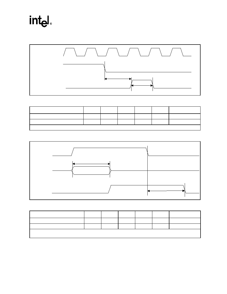
Dual-Speed Fast Ethernet Transceiver -- LXT970A
Datasheet
59
Figure 30. 10BASE-T SQE (Heartbeat) Timing
Table 39. 10BASE-T SQE (Heartbeat) Timing Parameters
Parameter
Sym
Min
Typ
1
Max
Units
Test Conditions
COL (SQE) Delay after TX_EN off
t9A
0.65
1.0
1.6
�
s
COL (SQE) Pulse duration
t9B
.5
1.0
1.5
�
s
1. Typical values are at 25 �C and are for design aid only; not guaranteed and not subject to production testing.
Figure 31. 10BASE-T Jab and Unjab Timing
Table 40. 10BASE-T Jab and Unjab Timing Parameters
Parameter
Sym
Min
Typ
1
Max
Units
Test Conditions
Maximum Transmit time
t10A
20
96 - 128
2
150
ms
Unjab time
t10B
250
525
750
ms
1. Typical values are at 25 �C and are for design aid only; not guaranteed and not subject to production testing.
2. Typical transmit time may be either of these values depending on internal 32 ms clock synchronization.
TX_CLK
TX_EN
t
9A
t
9B
COL
TXD
COL
t
10A
t
10B
TX_EN
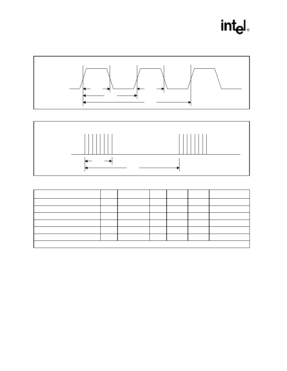
LXT970A -- Dual-Speed Fast Ethernet Transceiver
60
Datasheet
Figure 32. Auto Negotiation and Fast Link Pulse Timing
Figure 33. Fast Link Pulse Timing
Table 41. Auto Negotiation and Fast Link Pulse Timing Parameters
Parameter
Sym
Min
Typ
1
Max
Units
Test Conditions
Clock/Data pulse width
t1
�
100
�
ns
Clock pulse to Data pulse
t2
55.5
62.5
69.5
�
s
Clock pulse to Clock pulse
t3
111
125
139
�
s
FLP burst width
t4
�
2
�
ms
FLP burst to FLP burst
t5
8
12
24
ms
Clock/Data pulses per burst
�
17
�
33
ea
1. Typical values are at 25 �C and are for design aid only; not guaranteed and not subject to production testing.
TPOP
t1
t1
t2
t3
Clock Pulse
Data Pulse
Clock Pulse
TPOP
t4
t5
FLP Burst
FLP Burst
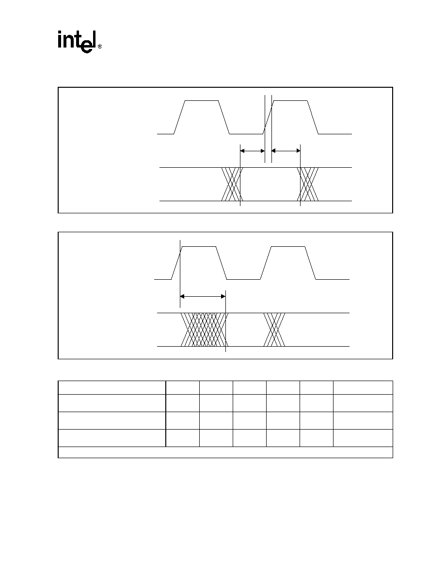
Dual-Speed Fast Ethernet Transceiver -- LXT970A
Datasheet
61
Figure 34. MDIO Timing when Sourced by STA
Figure 35. MDIO Timing when Sourced by PHY
Table 42. MDIO Timing Parameters
Parameter
Sym
Min
Typ
1
Max
Units
Test Conditions
MDIO Setup before MDC
�
10
�
�
ns
When sourced by
STA
MDIO Hold after MDC
�
10
�
�
ns
When sourced by
STA
MDC to MDIO Output delay
�
0
10
300
ns
When sourced by
PHY
1. Typical values are at 25� C and are for design aid only; not guaranteed and not subject to production testing.
10 ns
(Min)
MDC
MDIO
10 ns
(Min)
0 - 300 ns
MDC
MDIO
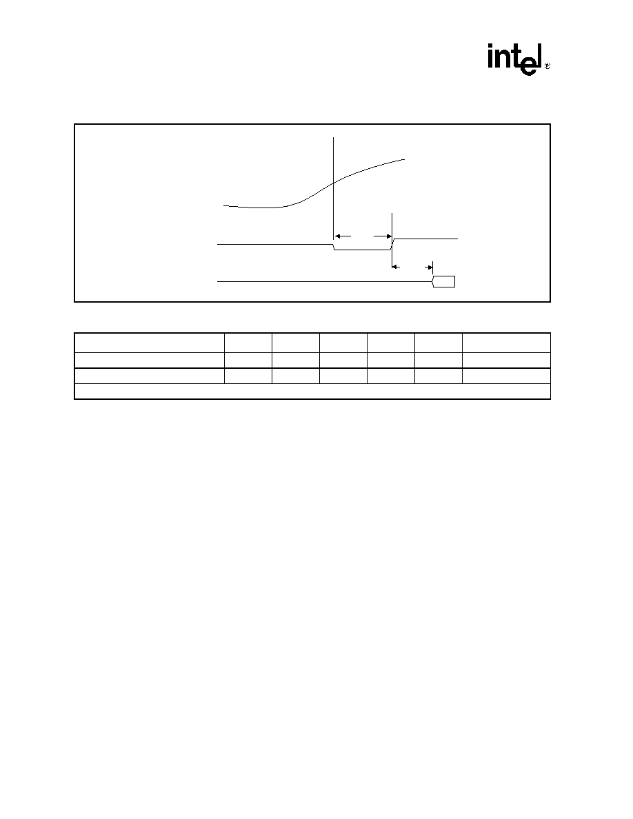
LXT970A -- Dual-Speed Fast Ethernet Transceiver
62
Datasheet
Figure 36. Power-Down Recovery Timing (Over Recommended Range)
Table 43. Power-Down Recovery Timing Parameters
Parameter
Sym
Min
Typ
1
Max
Units
Test Conditions
Power-Down recovery time
t
PDR
�
1.0
�
ms
Hardware reset time
t
HR
�
300
�
�
s
1. Typical values are at 25� C and are for design aid only; not guaranteed and not subject to production testing.
tPDR
VCC
RESET
MDIO,etc
VCC = 4.75V
tHR

Dual-Speed Fast Ethernet Transceiver -- LXT970A
Datasheet
63
5.0
Register Definitions
The LXT970A register set includes a total of twelve 16-bit registers. Refer to
Table 44
for a
complete register listing.
�
Seven base registers (0 through 6) are defined in accordance with the "Reconciliation Sublayer
and Media Independent Interface" and "Physical Layer Link Signalling for 10/100 Mbps
Auto-Negotiation" sections of the IEEE 802.3 specification (Register 7, Next Page, is not
supported).
�
Five additional registers (16 through 20) are defined in accordance with the IEEE 802.3
specification for adding unique chip functions.
Table 44. Register Set
Address
Register Name
Bit Assignments
0
Control Register
Refer to
Table 45 on page 64
1
Status Register
Refer to
Table 46 on page 65
2
PHY Identification Register 1
Refer to
Table 47 on page 66
3
PHY Identification Register 2
Refer to
Table 48 on page 66
4
Auto-Negotiation Advertisement Register
Refer to
Table 49 on page 67
5
Auto-Negotiation Link Partner Ability Register
Refer to
Table 50 on page 68
6
Auto-Negotiation Expansion Register
Refer to
Table 51 on page 69
16
Mirror Register
Refer to
Table 52 on page 69
17
Interrupt Enable Register
Refer to
Table 53 on page 70
18
Interrupt Status Register
Refer to
Table 54 on page 70
19
Configuration Register
Refer to
Table 55 on page 71
20
Chip Status Register
Refer to
Table 56 on page 72

LXT970A -- Dual-Speed Fast Ethernet Transceiver
64
Datasheet
Table 45. Control Register (Address 0)
Bit
Name
Description
Type
1
Default
0.15
Reset
1 = Reset chip.
0 = Enable normal operation.
R/W
SC
0
0.14
Loopback
1 = Enable loopback mode. When Loopback is enabled, during 100
Mbps operation, the LXT970A disconnects its transmitter and receiver
from the network. Data sent by the controller passes through the chip
and then gets looped back to the MII. During 10 Mbps operation the
preamble, SFD, and data loop directly back to the MII.
0 = Disable loopback mode.
R/W
0
0.13
Speed
Selection
1 = 100 Mbps
0 = 10 Mbps
R/W
Note 2
0.12
Auto-
Negotiation
Enable
1 = Enable auto-negotiate process (overrides speed select and duplex
mode bits).
0 = Disable auto-negotiate process.
R/W
Note 3
0.11
Power Down
1 = Enable power down.
0 = Enable normal operation.
R/W
Note 4
0.10
Isolate
1 = Electrically isolate LXT970A from MII.
0 = Normal operation.
R/W
Note 5
0.9
Restart Auto-
Negotiation
1 = Restart auto-negotiation process.
0 = Normal operation.
R/W
SC
Note 6
0.8
Duplex Mode
1 = Enable full-duplex.
0 = Enable half-duplex.
R/W
Note 7
0.7
Collision Test
1 = Enable COL signal test. Bit 0.14 must be enabled to use this bit.
This bit is used in conjunction with bit 0.14 to test the COL output.
0 = Disable COL signal test.
R/W
0 Note
8
0.6:4
Transceiver
Test Mode
Not Supported.
RO
0
0.3
Master-Slave
Enable
Not Supported.
RO
0
0.2
Master-Slave
Value
Not Supported.
RO
0
0.1:0
Reserved
R/W
0
1. R/W = Read/Write
SC = Self Clearing
2. If auto-negotiation is enabled, this bit is ignored. If auto-negotiation is disabled, the default value of bit 0.13 is determined by
pin CFG0.
3. The default value of bit 0.12 is determined by pin MF0.
4. The LXT970A internally maintains all set values of the configuration registers upon exiting power-down mode. A delay of 500
ns minimum is required from the time power down is cleared until any register can be written.
5. The default value of bit 0.10 is determined by pin TRSTE.
6. If auto-negotiation is enabled, the default value of bit 0.9 is determined by pin CFG0. If auto-negotiation is disabled, the
default value of
bit 0.9 = 0.
7. If auto-negotiation is enabled, this bit is ignored. If auto-negotiation is disabled, the default value of bit 0.8 is determined by
pin FDE.
8. This bit is ignored unless loopback is enabled (0.14 = 1).

Dual-Speed Fast Ethernet Transceiver -- LXT970A
Datasheet
65
Table 46. Status Register (Address 1)
Bit
Name
Description
Type
1
Default
1.15
100BASE-T4
Not Supported.
RO
0
1.14
100BASE-X
full-duplex
1 = LXT970A able to perform full-duplex 100BASE-X.
RO
1
1.13
100BASE-X
half-duplex
1 = LXT970A able to perform half-duplex 100BASE-X.
RO
1
1.12
10 Mb/s
full-duplex
1 = LXT970A able to operate at 10 Mb/s in full-duplex mode.
RO
1
1.11
10 Mb/s
half-duplex
1 = LXT970A able to operate at 10 Mb/s in half-duplex mode.
RO
1
1.10
100BASE-T2
full-duplex
Not Supported.
RO
0
1.9
100BASE-T2
half-duplex
Not Supported.
RO
0
1.8
Reserved
Ignore on read.
RO
0
1.7
Master-Slave
Configuration
Fault
Not Supported.
RO
0
1.6
MF Preamble
Suppression
0 = LXT970A will not accept management frames with preamble
suppressed.
RO
0
1.5
Auto-Neg.
Complete
1 = Auto-negotiation process complete.
0 = Auto-negotiation process not complete.
RO
0
1.4
Remote Fault
1 = Remote fault condition detected.
0 = No remote fault condition detected.
This bit is set when:
Link partner transmits a remote fault condition (bit 5.13 = 1)
Link partner protocol is anything other than CSMA-CD
(bits 5.4:0 = <00001>)
Link partner advertises T4 capability only
(bits 5.9:5
�
<10000>)
RO/LH
0
1.3
Auto-Neg.
Ability
1 = LXT970A is able to perform auto-negotiation.
RO
1
1.2
Link Status
1 = Link is up.
0 = Link is down.
RO/LL
0
1.1
Jabber Detect
(10BASE-T
Only)
1 = Jabber condition detected.
0 = No jabber condition detected.
RO/LH
0
1.0
Extended
Capability
1 = Extended register capabilities.
RO
1
1. RO = Read Only
LL = Latching Low (This bit remains Low until read, and then returns High).
LH = Latching High (This bit remains High until read, and then returns Low).
LXT970A -- Dual-Speed Fast Ethernet Transceiver
66
Datasheet
Table 47. PHY Identification Register 1 (Address 2)
Bit
Name
Description
Type
1
Default
2.15:0
PHY ID
Number
The PHY identifier composed of bits 3 through 18 of the OUI.
RO
7810 hex
1. RO = Read Only
Table 48. PHY Identification Register 2 (Address 3)
Bit
Name
Description
Type
1
Default
3.15:10
PHY ID number
The PHY identifier composed of bits 19 through 24 of the OUI.
RO
000000 bin
3.9:4
Manufacturer's
model number
6 bits containing manufacturer's part number.
RO
000000 bin
3.3:0
Manufacturer's
revision number
4 bits containing manufacturer's revision number.
RO
0011 bin
1. RO = Read Only
Figure 37. PHY Identifier Bit Mapping
a b c r s x
Organizationally Unique Identifier
1 2 3 18 19 24
PHY ID Register 1
15 14 13 12 11 10 9
8
7
6
5
4
3
2
1
0
PHY ID Register 2
15 14 13 12 11 10 9
8
7
6
5
4
3
2
1
0
Manufacturers Revision
Part Number Number
5 4 3 2 1 0 3 2 1 0
The Intel OUI is 00207B hex.

Dual-Speed Fast Ethernet Transceiver -- LXT970A
Datasheet
67
Table 49. Auto Negotiation Advertisement Register (Address 4)
Bit
Name
Description
Type
1
Default
4.15
Next Page
Not Supported
RO
0
4.14
Reserved
Ignore on read.
RO
0
4.13
Remote Fault
1 = Remote fault.
0 = No remote fault.
R/W
0
4.12:11
Reserved
Ignore on read.
R/W
0
4.10
Pause
1 = Pause operation is enabled for full-duplex links.
0 = Pause operation is disabled.
R/W
0
4.9
100BASE-T4
1 = 100BASE-T4 capability is available.
0 = 100BASE-T4 capability is not available.
(The LXT970A does not support 100BASE-T4, but allows this bit to be set
to advertise in the Auto-Negotiation sequence for 100BASE-T4 operation.
An external 100BASE-T4 transceiver could be switched in if this capability
is desired.)
R/W
0
4.8
100BASE-TX
full-duplex
1 = DTE is 100BASE-TX full-duplex capable.
0 = DTE is not 100BASE-TX full-duplex capable.
R/W
Note 2
4.7
100BASE-TX
1 = DTE is 100BASE-TX capable.
0 = DTE is not 100BASE-TX capable.
R/W
Note 3
4.6
10BASE-T
full-duplex
1 = DTE is 10BASE-T full-duplex capable.
0 = DTE is not 10BASE-T full-duplex capable.
R/W
Note 4
4.5
10BASE-T
1 = DTE is 10BASE-T capable.
0 = DTE is not 10BASE-T capable.
R/W
Note 5
4.4:0
Selector Field,
S<4:0>
<00001> = IEEE 802.3
<00010> = IEEE 802.9 ISLAN-16T
<00000> = Reserved for future Auto-Negotiation development
<11111> = Reserved for future Auto-Negotiation development
Unspecified or reserved combinations should not be transmitted.
R/W
00001
1. R/W = Read/Write
RO = Read Only
2. The default value of bit 4.8 is determined by pin FDE AND'ed with pin MF4.
3. The default value of bit 4.7 is determined by pin MF4.
4. The default value of bit 4.6 is determined by pin FDE AND'ed with pin CFG1.
5. The default value of bit 4.5 is determined by pin CFG1.

LXT970A -- Dual-Speed Fast Ethernet Transceiver
68
Datasheet
Table 50. Auto Negotiation Link Partner Ability Register (Address 5)
Bit
Name
Description
Type
1
Default
5.15
Next Page
1 = Link Partner has ability to send multiple pages.
0 = Link Partner has no ability to send multiple pages.
RO
N/A
5.14
Acknowledge
1 = Link Partner has received Link Code Word from LXT970A.
0 = Link Partner has not received Link Code Word from LXT970A.
RO
N/A
5.13
Remote Fault
1 = Remote fault.
0 = No remote fault.
RO
N/A
5.12:11
Reserved
Ignore on read.
RO
N/A
5.10
Pause
1 = Pause operation is enabled for link partner.
0 = Pause operation is disabled.
RO
N/A
5.9
100BASE-T4
1 = Link Partner is 100BASE-T4 capable.
0 = Link Partner is not 100BASE-T4 capable.
RO
N/A
5.8
100BASE-TX
full-duplex
1 = Link Partner is 100BASE-TX full-duplex capable.
0 = Link Partner is not 100BASE-TX full-duplex capable.
RO
N/A
5.7
100BASE-TX
1 = Link Partner is 100BASE-TX capable.
0 = Link Partner is not 100BASE-TX capable.
RO
N/A
5.6
10BASE-T
full-duplex
1 = Link Partner is 10BASE-T full-duplex capable.
0 = Link Partner is not 10BASE-T full-duplex capable.
RO
N/A
5.5
10BASE-T
1 = Link Partner is 10BASE-T capable.
0 = Link Partner is not 10BASE-T capable.
RO
N/A
5.4:0
Selector Field
S[4:0]
<00001> = IEEE 802.3
<00010> = IEEE 802.9 ISLAN-16T
<00000> = Reserved for future Auto-Negotiation development
<11111> = Reserved for future Auto-Negotiation development
Unspecified or reserved combinations shall not be transmitted.
RO
N/A
1. RO = Read Only
Dual-Speed Fast Ethernet Transceiver -- LXT970A
Datasheet
69
Table 51. Auto Negotiation Expansion (Address 6)
Bit
Name
Description
Type
1
Default
6.15:5
Reserved
Ignore.
RO
0
6.4
Parallel
Detection Fault
1 = Parallel detection fault has occurred.
0 = Parallel detection fault has not occurred.
RO/
LH
0
6.3
Link Partner
Next Page Able
1 = Link partner is next page able.
0 = Link partner is not next page able.
RO
0
6.2
Next Page Able
Not Supported.
RO
0
6.1
Page Received
1 = 3 identical and consecutive link code words have been received from
link partner.
0 = 3 identical and consecutive link code words have not been received
from link partner.
RO/
LH
0
6.0
Link Partner
Auto Neg Able
1 = Link partner is auto-negotiation able.
0 = Link partner is not auto-negotiation able.
RO
0
1. RO = Read Only
LH = Latching High (This bit remains High until read, and then returns Low).
Table 52. Mirror Register (Address 16, Hex 10)
Bit
Name
Description
Type
1
Default
16.15:0
User Defined
This register is intended for use in checking the MII serial port and has no
effect on chip operation.
R/W
0
1. R/W = Read /Write

LXT970A -- Dual-Speed Fast Ethernet Transceiver
70
Datasheet
Table 53. Interrupt Enable Register (Address 17, Hex 11)
Bit
Name
Description
Type
1
Default
17.15:4
Reserved
Write as 0; ignore on read.
R/W
N/A
17.3
MIIDRVLVL
1 = Reduced MII driver levels. Pull-down strength of the MII driver is
reduced by a factor of 10, and the pull-up strength is reduced by a factor
of 8. Reduced driver levels on the MII I/O pins are recommended for
managed multi-port applications.
0 = High-strength MII driver levels that can effectively source 50 - 60 mA.
Series termination resistors (55
)
are recommended on all output
signals when using this level to avoid undershoot or overshoot.
R/W
0
17.2
LNK
CRITERIA
1 = Enhanced link loss criteria. Link loss criteria is independent of symbol
error rate. Loss of scrambler lock for more than 1 - 2 msec will brings the
link down. Link up criteria is based on symbol error rate.
0 = Standard link criteria. Both link up and link loss are based on symbol
error rate.
R/W
0
17.1
INTEN
1 = Enable interrupts. Must be enabled for bit 17.0 or 19.12 to be
effective.
0 = Disable interrupts.
R/W
0
17.0
TINT
1 = Forces MDINT Low and sets bit 18.15 = 1. Also forces interrupt
pulse on MDIO when bit 19.12 = 1.
0 = Normal operation.
This bit is ignored unless the interrupt function is enabled (17.1 = 1).
R/W
0
1. R/W = Read /Write
Table 54. Interrupt Status Register (Address 18, Hex 12)
Bit
Name
Description
Type
1
Default
18.15
MINT
1 = Indicates MII interrupt pending.
0 = Indicates no MII interrupt pending. This bit is cleared by reading
Register 1 followed by reading Register 18.
RO
N/A
18.14
XTALOK
1 = Indicates that the LXT970A is fully powered up and the on-chip clocks
are stable.
0 = Indicates that XTAL circuit is not stable.
RO
0
18.13:0
Reserved
Ignore
RO
0
1. RO = Read Only

Dual-Speed Fast Ethernet Transceiver -- LXT970A
Datasheet
71
Table 55. Configuration Register (Address 19, Hex 13)
Bit
Name
Description
Type
1
Default
19.15
Reserved
Write as 0; ignore on read.
R/W
N/A
19.14
Txmit Test
(100BASE-TX)
1 = 100BASE-T transmit test enabled, LXT970A transmits data
regardless of link status. This function is the analog of the link test
function (19.8) for 100BASE-TX.
0 = Normal operation.
R/W
0
19.13
Repeater Mode
1 = Enable Repeater Mode.
0 = Enable DTE Mode.
R/W
Note 2
19.12
MDIO_INT
1 = Enable interrupt signaling on MDIO (if 17.1 = 1).
0 = Normal operation (MDIO Interrupt disabled).
Bit is ignored unless the interrupt function is enabled
(17.1 = 1).
R/W
0
19.11
TP Loopback
(10BASE-T)
1 = Disable 10BT TP Loopback. Data transmitted by the MAC will not
loopback to the RXD, RX_DV, and CRS pins.
0 = Enable 10BT TP Loopback - Preamble, SFD, and data are directly
looped back to the MII.
R/W
0
19.10
SQE
(10BASE-T)
1 = Enable SQE.
0 = Disable SQE (Default).
R/W
0
19.9
Jabber
(10BASE-T)
1 = Disable jabber.
0 = Normal operation (jabber enabled).
R/W
0
19.8
Link Test
(10BASE-T)
1 = Disable 10BASE-T link integrity test.
0 = Normal operation (10BASE-T link integrity test enabled).
R/W
Note 3
19.7:6
LEDC
Programming bits
Determine condition indicated by LEDC.
bit 7 bit 6 Description
0 0 LEDC indicates collision
0 1 LEDC is off
1 0 LEDC indicates activity.
1 1 LEDC is continuously on (for diagnostic use).
R/W
0,0
19.5
Advance TX Clock
1 = TX clock is advanced relative to TXD<4:0> and TX_ER by 1/2
TX_CLK cycle.
0 = Normal operation.
R/W
0
19.4
5B Symbol/
(100BASE-X only)
4B Nibble
1 = 5-bit Symbol Mode (Bypass encoder/decoder);
RXD<4:0> symbol data is not aligned.
0 = 4-bit Nibble Mode (Normal operation).
R/W
Note 4
19.3
Scrambler
(100BASE-X only)
1 = Bypass transmit scrambler and receive descrambler.
0 = Normal operation (scrambler and descrambler enabled).
In FX mode, the LXT970A automatically bypasses the Scrambler.
Selecting Scrambler bypass in FX mode causes the LXT970A to also
bypass the 4B/5B encoder and enable Symbol mode MII operation.
R/W
Note 5
1. R/W = Read/Write
2. The default value of bit 19.13 is determined by pin MF1.
3. If auto-negotiation is disabled, the default value of bit 19.8 is determined by pin CFG1. If auto-neg is enabled, the default
value of bit 19.8 = 0.
4. The default value of bit 19.4 is determined by pin MF2 Operation.
5. The default value of bit 19.3 is determined by pin MF3 Operation.
6. If auto-negotiation is disabled, default value of bit 19.2 is determined by pin MF4. If auto-negotiation is enabled, default value
of bit 19.2 = 0.
LXT970A -- Dual-Speed Fast Ethernet Transceiver
72
Datasheet
19.2
100BASE-FX
1 = Enable 100BASE fiber interface.
0 = Enable 100BASE twisted-pair interface.
R/W
Note 6
19.1
Reserved
Write as 0; Ignore on read.
R/W
0
19.0
Transmit
Disconnect
1 = Disconnect TP transmitter from line.
0 = Normal operation.
R/W
0
Table 56. Chip Status Register (Address 20, Hex 14)
Bit
Name
Description
Type
1
Default
20.15:1
4
Reserved
Ignore on read.
RO
N/A
20.13
Link
1 = Link is up.
0 = Link is down.
Link bit 20.13 is a duplicate of bit 1.2, except that it is a dynamic
indication, whereas bit 1.2 latches Low.
RO
0
20.12
Duplex Mode
1 = Full-duplex.
0 = Half-duplex.
RO
Note 2
20.11
Speed
1 = 100 Mbps operation.
0 = 10 Mbps operation.
RO
Note 2
20.10
Reserved
Ignore on read.
RO
N/A
20.9
Auto-Negotiation
Complete
1 = Auto-negotiation process complete.
0 = Auto-negotiation process not complete.
Auto-Negotiation Complete bit 20.9 is a duplicate of bit 1.5.
RO/LH
0
20.8
Page Received
1 = Three identical and consecutive link code words have been
received.
0 = Three identical and consecutive link code words have not been
received.
Page Received bit 20.8 is a duplicate of bit 6.1
RO/LH
0
20:7
Reserved
Ignore on read.
RO
0
20.6
Reserved
Ignore on read.
RO
0
20.5
Reserved
Ignore on read.
RO
N/A
20.4
Reserved
Ignore on read.
RO
N/A
20.3
Reserved
Ignore on read.
RO
N/A
20.2
Low-Voltage
1 = Low-voltage fault on VCC has occurred.
0 = No fault.
RO
N/A
20.1
Reserved
Ignore on read.
RO
N/A
20.0
Reserved
Ignore on read.
RO
N/A
1. RO = Read Only
LH = Latching High (This bit remains High until read, and then returns Low).
2. Bits 20.12 and 20.11 reflect the current operating mode of the LXT970A.
Table 55. Configuration Register (Address 19, Hex 13) (Continued)
Bit
Name
Description
Type
1
Default
1. R/W = Read/Write
2. The default value of bit 19.13 is determined by pin MF1.
3. If auto-negotiation is disabled, the default value of bit 19.8 is determined by pin CFG1. If auto-neg is enabled, the default
value of bit 19.8 = 0.
4. The default value of bit 19.4 is determined by pin MF2 Operation.
5. The default value of bit 19.3 is determined by pin MF3 Operation.
6. If auto-negotiation is disabled, default value of bit 19.2 is determined by pin MF4. If auto-negotiation is enabled, default value
of bit 19.2 = 0.
Dual-Speed Fast Ethernet Transceiver -- LXT970A
Datasheet
73
6.0
Mechanical Specifications
Figure 38. 64-Pin QFP Package Diagram
Dim
Millimeters
Min
Max
A
�
3.30
A
1
0.000
0.25
A
2
2.55
3.05
B
0.30
0.45
D
17.65
18.15
D
1
13.95
14.05
D
3
12.00
REF
E
17.65
18.15
E
1
13.95
14.05
E
3
12.00
REF
e
0.80
BSC
L
0.73
1.03
L
1
1.95
REF
3
5�
16�
0�
7�
64-Pin Quad Flat Pack
�
Part Number - LXT970AQC
�
Commercial Temperature Range (0 to +70�C)
A
1
A
2
L
A
B
L
1
3
3
D
D
1
E
E
1
e
/
2
e
E
3
D
3
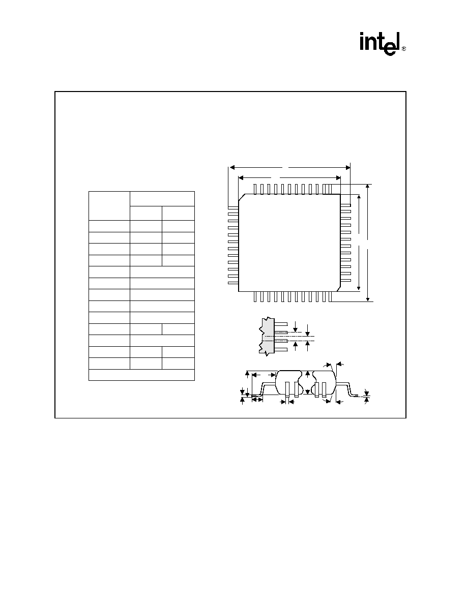
LXT970A -- Dual-Speed Fast Ethernet Transceiver
74
Datasheet
Figure 39. 64-Pin TQFP Package Diagram
64-Pin Thin Quad Flat Pack
�
Part Number - LXT970ATC
�
Commercial Temperature Range (0 to +70�C)
Dim
Millimeters
Min
Max
A
�
1.20
A
1
0.05
0.15
A
2
0.95
1.05
B
0.17
0.27
D
12.0 REF
D
1
10.0 REF
E
12.0 REF
E1
10.0 REF
e
0.50 REF
L
0.45
0.75
L
1
1.00 REF
3
11
o
13
o
0
o
7
o
1. Basic Spacing between Centers.
D
D
1
A
1
A
2
L
A
B
L
1
3
3
E
E
1
e
/
2
e