November 1994
CAUTION: These devices are sensitive to electrostatic discharge. Users should follow proper I.C. Handling Procedures.
Copyright
©
Harris Corporation 1992
1
S E M I C O N D U C T O R
2N7288D, 2N7288R
2N7288H
Radiation Hardened
N-Channel Power MOSFETs
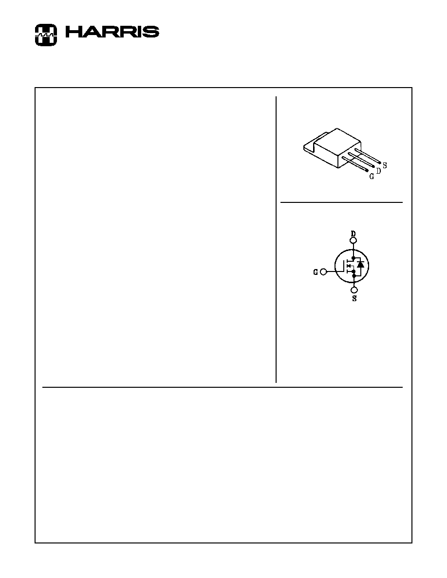
Package
TO-257AA
Symbol
Features
∑ 9A, 250V, RDS(on) = 0.415
∑ Second Generation Rad Hard MOSFET Results From New Design Concepts
∑ Gamma
- Meets Pre-Rad Specifications to 100KRAD(Si)
- Defined End Point Specs at 300KRAD(Si) and 1000KRAD(Si)
- Performance Permits Limited Use to 3000KRAD(Si)
∑ Gamma Dot
- Survives 3E9RAD(Si)/sec at 80% BVDSS Typically
- Survives 2E12 Typically If Current Limited to IDM
∑ Photo Current
- 7.0nA Per-RAD(Si)/sec Typically
∑ Neutron
- Pre-RAD Specifications for 1E13 Neutrons/cm
2
- Usable to 1E14 Neutrons/cm
2
∑ Single Event
- Typically Survives 1E5ions/cm
2
Having an
LET
35MeV/mg/cm
2
and a Range
30
µ
m at 80% BVDSS
Description
The Harris Semiconductor Sector has designed a series of SECOND GENERA-
TION hardened power MOSFETs of both N and P channel enhancement types
with ratings from 100V to 500V, 1A to 60A, and on resistance as low as 25m
.
Total dose hardness is offered at 100K RAD(Si) and 1000KRAD(Si) with neutron
hardness ranging from 1E13n/cm
2
for 500V product to 1E14n/cm
2
for 100V prod-
uct. Dose rate hardness (GAMMA DOT) exists for rates to 1E9 without current lim-
iting and 2E12 with current limiting. Heavy ion survival from signal event drain
burn-out exists for linear energy transfer (LET) of 35 at 80% of rated voltage.
This MOSFET is an enhancement-mode silicon-gate power field effect transistor of
the vertical DMOS (VDMOS) structure. It is specially designed and processed to
exhibit minimal characteristic changes to total dose (GAMMA) and neutron (n
o
)
exposures. Design and processing efforts are also directed to enhance survival to
heavy ion (SEE) and/or dose rate (GAMMA DOT) exposure.
This part may be supplied as a die or in various packages other than shown above.
Reliability screening is available as either non TX (commercial), TX equivalent of
MIL-S-19500, TXV equivalent of MIL-S-19500, or space equivalent of MIL-S-
19500. Contact the Harris Semiconductor High-Reliability Marketing group for any
desired deviations from the data sheet.
File Number
3256.1
REGISTRATION PENDING
Available as FRS244 (D, R, H)
Absolute Maximum Ratings
(TC = +25
o
C) Unless Otherwise Specified
2N7288D, R, H
UNITS
Drain-Source Voltage. . . . . . . . . . . . . . . . . . . . . . . . . . . . . . . . . . . . . . . . . . . . . . . . . . . . . . . VDS
250
V
Drain-Gate Voltage (RGS = 20k
) . . . . . . . . . . . . . . . . . . . . . . . . . . . . . . . . . . . . . . . . . . VDGR
250
V
Continuous Drain Current
TC = +25
o
C . . . . . . . . . . . . . . . . . . . . . . . . . . . . . . . . . . . . . . . . . . . . . . . . . . . . . . . . . . . . . .ID
TC = +100
o
C . . . . . . . . . . . . . . . . . . . . . . . . . . . . . . . . . . . . . . . . . . . . . . . . . . . . . . . . . . . . .ID
9
6
A
A
Pulsed Drain Current . . . . . . . . . . . . . . . . . . . . . . . . . . . . . . . . . . . . . . . . . . . . . . . . . . . . . . . IDM
27
A
Gate-Source Voltage . . . . . . . . . . . . . . . . . . . . . . . . . . . . . . . . . . . . . . . . . . . . . . . . . . . . . . .VGS
±
20
V
Maximum Power Dissipation
TC = +25
o
C . . . . . . . . . . . . . . . . . . . . . . . . . . . . . . . . . . . . . . . . . . . . . . . . . . . . . . . . . . . . . PT
TC = +100
o
C . . . . . . . . . . . . . . . . . . . . . . . . . . . . . . . . . . . . . . . . . . . . . . . . . . . . . . . . . . . . PT
Derated Above +25
o
C . . . . . . . . . . . . . . . . . . . . . . . . . . . . . . . . . . . . . . . . . . . . . . . . . . . . . . .
75
30
0.60
W
W
W/
o
C
Inductive Current, Clamped, L = 100
µ
H, (See Test Figure). . . . . . . . . . . . . . . . . . . . . . . . . . ILM
27
A
Continuous Source Current (Body Diode) . . . . . . . . . . . . . . . . . . . . . . . . . . . . . . . . . . . . . . . . . IS
9
A
Pulsed Source Current (Body Diode) . . . . . . . . . . . . . . . . . . . . . . . . . . . . . . . . . . . . . . . . . . ISM
27
A
Operating And Storage Temperature . . . . . . . . . . . . . . . . . . . . . . . . . . . . . . . . . . . . . TJC, TSTG
-55 to +150
o
C
Lead Temperature (During Soldering)
Distance > 0.063 in. (1.6mm) From Case, 10s Max. . . . . . . . . . . . . . . . . . . . . . . . . . . . . . . TL
300
o
C
2
Specifications 2N7288D, 2N7288R, 2N7288H - Registration Pending
Pre-Radiation Electrical Specifications
TC = +25
o
C, Unless Otherwise Specified
PARAMETER
SYMBOL
TEST CONDITIONS
LIMITS
UNITS
MIN
MAX
Drain-Source Breakdown Volts
BVDSS
VGS = 0, ID = 1mA
250
-
V
Gate-Threshold Volts
VGS(th)
VDS = VGS, ID = 1mA
2.0
4.0
V
Gate-Body Leakage Forward
IGSSF
VGS = +20V
-
100
nA
Gate-Body Leakage Reverse
IGSSR
VGS = -20V
-
100
nA
Zero-Gate Voltage
Drain Current
IDSS1
IDSS2
IDSS3
VDS = 250V, VGS = 0
VDS = 200V, VGS = 0
VDS = 200V, VGS = 0, TC = +125
o
C
-
-
-
1
0.025
0.25
mA
Rated Avalanche Current
IAR
Time = 20
µ
s
-
27
A
Drain-Source On-State Volts
VDS(on)
VGS = 10V, ID = 9A
-
3.92
V
Drain-Source On Resistance
RDS(on)
VGS = 10V, ID = 6A
-
0.415
Turn-On Delay Time
td(on)
VDD = 125V, ID = 9A
-
46
ns
Rise Time
tr
Pulse Width = 3
µ
s
-
100
Turn-Off Delay Time
td(off)
Period = 300
µ
s, Rg = 25
-
368
Fall Time
tf
0
VGS
10 (See Test Circuit)
-
124
Gate-Charge Threshold
QG(th)
VDD = 125V, ID = 9A
IGS1 = IGS2
0
VGS
20
2
8
nc
Gate-Charge On State
QG(on)
29
116
Gate-Charge Total
QGM
55
220
Plateau Voltage
VGP
2
10
V
Gate-Charge Source
QGS
4
18
nc
Gate-Charge Drain
QGD
12
48
Diode Forward Voltage
VSD
ID = 9A, VGD = 0
0.6
1.8
V
Reverse Recovery Time
TT
I = 9A; di/dt = 100A/
µ
s
-
840
ns
Junction-To-Case
R
jc
-
1.67
o
C/W
Junction-To-Ambient
R
ja
Free Air Operation
-
60
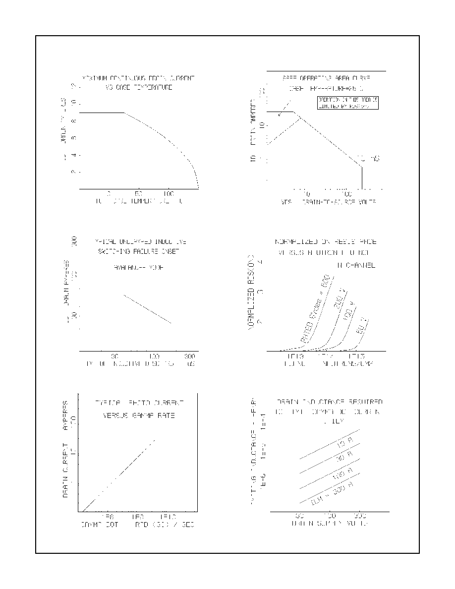
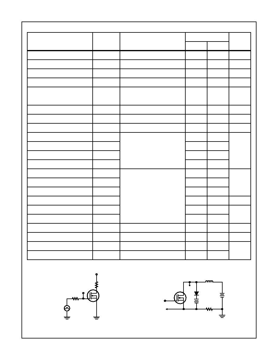
FIGURE 1. SWITCHING TIME TESTING
FIGURE 2. CLAMPED INDUCTIVE SWITCHING, ILM
VDD
RL
V1
Rg
VDS
DUT
IL
VC
E1
L
0.06
E1 = 0.5 BVDSS
VC = 0.75 BVDSS
3
Specifications 2N7288D, 2N7288R, 2N7288H - Registration Pending
Post-Radiation Electrical Specifications
TC = +25
o
C, Unless Otherwise Specified
PARAMETER
SYMBOL
TYPE
TEST CONDITIONS
LIMITS
UNITS
MIN
MAX
Drain-Source
Breakdown Volts
(Note 4, 6)
BVDSS
2N7288D, R
VGS = 0, ID = 1mA
250
-
V
(Note 5, 6)
BVDSS
2N7288H
VGS = 0, ID = 1mA
238
-
V
Gate-Source
Threshold Volts
(Note 4, 6)
VGS(th)
2N7288D, R
VGS = VDS, ID = 1mA
2.0
4.0
V
(Note 3, 5, 6)
VGS(th)
2N7288H
VGS = VDS, ID = 1mA
1.5
4.5
V
Gate-Body
Leakage Forward
(Note 4, 6)
IGSSF
2N7288D, R
VGS = 20V, VDS = 0
-
100
nA
(Note 5, 6)
IGSSF
2N7288H
VGS = 20V, VDS = 0
-
200
nA
Gate-Body
Leakage Reverse
(Note 2, 4, 6)
IGSSR
2N7288D, R
VGS = -20V, VDS = 0
-
100
nA
(Note 2, 5, 6)
IGSSR
2N7288H
VGS = -20V, VDS = 0
-
200
nA
Zero-Gate Voltage
Drain Current
(Note 4, 6)
IDSS
2N7288D, R
VGS = 0, VDS = 200V
-
25
µ
A
(Note 5, 6)
IDSS
2N7288H
VGS = 0, VDS = 200V
-
100
µ
A
Drain-Source
On-State Volts
(Note 1, 4, 6)
VDS(on)
2N7288D, R
VGS = 10V, ID = 9A
-
3.92
V
(Note 1, 5, 6)
VDS(on)
2N7288H
VGS = 16V, ID = 9A
-
5.88
V
Drain-Source
On Resistance
(Note 1, 4, 6)
RDS(on)
2N7288D, R
VGS = 10V, ID = 6A
-
0.415
(Note 1, 5, 6)
RDS(on)
2N7288H
VGS = 14V, ID = 6A
-
0.623
NOTES:
1. Pulse test, 300
µ
s max
2. Absolute value
3. Gamma = 300KRAD(Si)
4. Gamma = 10KRAD(Si) for "D", 100KRAD(Si) for "R". Neutron = 1E13
5. Gamma = 1000KRAD(Si). Neutron = 1E13
6. Insitu Gamma bias must be sampled for both VGS = +10V, VDS = 0V and VGS = 0V, VDS = 80% BVDSS
7. Gamma data taken 1/30/90 on TA17643 devices by GE ASTRO SPACE; EMC/SURVIVABILITY LABORATORY; KING OF PRUSSIA,
PA 19401
8. Single event drain burnout testing by Titus, J.L., et al of NWSC, Crane, IN at Brookhaven Nat. Lab. Dec 11-14, 1989
9. Neutron derivation, HARRIS Application note AN-8831, Oct. 1988
5
2N7288D, 2N7288R, 2N7288H - Registration Pending
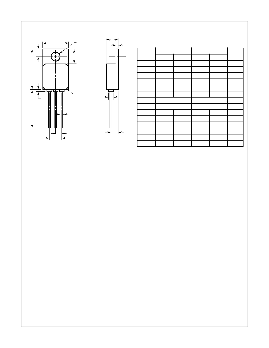
Packaging
NOTES:
1. These dimensions are within allowable dimensions of Rev. B of
JEDEC TO-257AA dated 9-88.
2. Add typically 0.002 inches (0.05mm) for solder coating.
3. Lead dimension (without solder).
4. Position of lead to be measured 0.150 inches (3.81mm) from bottom
of dimension D.
5. Die to base BeO isolated, terminals to case ceramic isolated.
6. Controlling dimension: Inch.
7. Revision 1 dated 1-93.
Q
D
L
H
1
b
e
e
1
A
1
E
A
J
1
0.065 R TYP.
ÿP
L
1
ÿb
1
1
2
3
TO-257AA
3 LEAD JEDEC TO-257AA HERMETIC METAL PACKAGE
SYMBOL
INCHES
MILLIMETERS
NOTES
MIN
MAX
MIN
MAX
A
0.190
0.200
4.83
5.08
-
A
1
0.035
0.045
0.89
1.14
-
ÿb
0.025
0.035
0.64
0.88
2, 3
ÿb
1
0.060
0.090
1.53
2.28
-
D
0.645
0.665
16.39
16.89
-
E
0.410
0.420
10.42
10.66
-
e
0.100 TYP
2.54 TYP
4
e
1
0.200 BSC
5.08 BSC
4
H
1
0.230
0.250
5.85
6.35
-
J
1
0.110
0.130
2.80
3.30
4
L
0.600
0.650
15.24
16.51
-
L
1
-
0.035
-
0.88
-
ÿP
0.140
0.150
3.56
3.81
-
Q
0.113
0.133
2.88
3.37
-