5-178
March 1997
HS-3182
ARINC 429 Bus Interface Line Driver Circuit
Features
∑ TTL and CMOS Compatible Inputs
∑ Adjustable Rise and Fall Times via Two External
Capacitors
∑ Programmable Output Differential Voltage via V
REF
Input
∑ Operates at Data Rates Up to 100 Kilobits/Sec
∑ Output Short Circuit Proof and Contains Over-Voltage
Protection
∑ Outputs are Inhibited (0 Volts) If DATA (A) and DATA
(B) Inputs are Both in the "Logic One" State
∑ DATA (A) and DATA (B) Signals are "AND'd" with Clock
and Sync Signals
∑ Full Military Temperature Range
Description
The HS-3182 is a monolithic dielectrically isolated bipolar differ-
ential line driver designed to meet the specifications of ARINC
429. This Device is intended to be used with a companion chip,
HS-3282 CMOS ARINC Bus Interface Circuit, which provides
the data formatting and processor interface function.
All logic inputs are TTL and CMOS compatible. In addition to
the DATA (A) and DATA (B) inputs, there are also inputs for
CLOCK and SYNC signals which are AND'd with the DATA
inputs. This feature enhances system performance and allows
the HS-3182 to be used with devices other than the HS-3182.
Three power supplies are necessary to operate the
HS-3182: +V = +15V
±
10%, -V = -15V
±
10%, and V
1
= 5V
±
5%. V
REF
is used to program the differential output voltage
swing such that V
OUT
(DIFF) =
±
2V
REF
. Typically, V
REF
=
V
1
= 5V
±
5%, but a separate power supply may be used for
V
REF
which should not exceed 6V.
The driver output impedance is 75
±
20% at 25
o
C. Driver
output rise and fall times are independently programmed
through the use of two external capacitors connected to the
C
A
and C
B
inputs. Typical capacitor values are C
A
= C
B
=
75pF for high-speed operation (100KBPS), and C
A
= C
B
=
300pF for low-speed operation (12 to 14.5KBPS). The out-
puts are protected against over-voltage and short circuit as
shown in the Block Diagram. The HS-3182 is designed to
operate with a case temperature range of -55
o
C to +125
o
C,
or 0
o
C to +70
o
C.
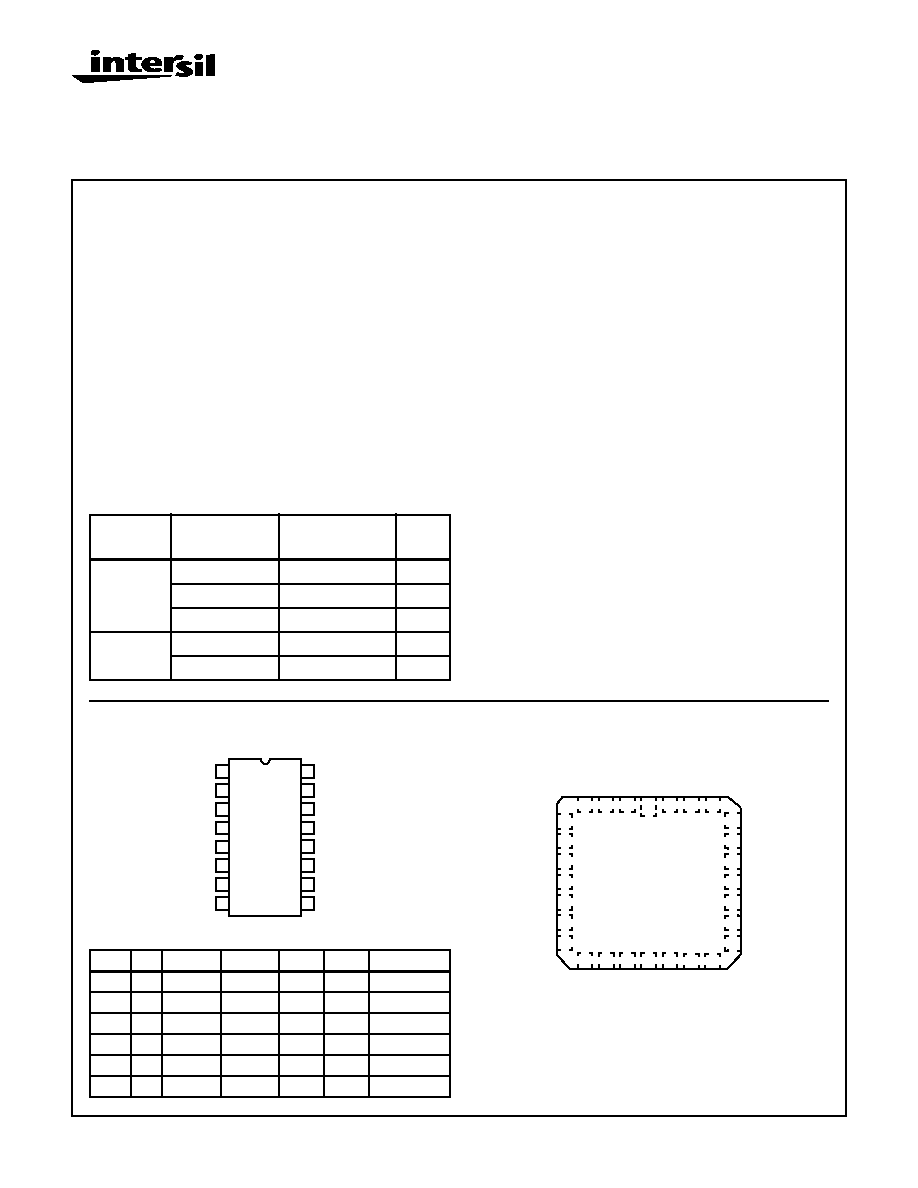
Pinouts
HS-3182 (SBDIP)
TOP VIEW
HS-3182 (CLCC)
TOP VIEW
Ordering Information
PACKAGE
TEMPERATURE
RANGE
PART NUMBER
PKG.
NO
SBDIP
-40
o
C to +85
o
C
HS1-3182-9+
D16.3
-55
o
C to +125
o
C
HS1-3182-8
D16.3
SMD#
-55
o
C to +125
o
C
5962-8687901EA
D16.3
CLCC
-55
o
C to +125
o
C
HS4-3182-8
J28.A
SMD#
-55
o
C to +125
o
C
5962-86879013A
J28.A
TRUTH TABLE
SYNC CLK DATA (A) DATA (B)
A
OUT
B
OUT
COMMENTS
X
L
X
X
0V
0V
Null
L
X
X
X
0V
0V
Null
H
H
L
L
0V
0V
Null
H
H
L
H
-V
REF
+V
REF
Low
H
H
H
L
+V
REF
-V
REF
High
H
H
H
H
0V
0V
Null
14
15
16
9
13
12
11
10
1
2
3
4
5
7
6
8
V
REF
GND
SYNC
DATA (A)
C
A
A
OUT
GND
-V
V
1
CLK
DATA (B)
C
B
B
OUT
NC
+V
NC
23
24
25
22
21
20
19
11
3
2
1
4
14
15 16 17 18
12 13
28 27 26
10
5
6
7
8
9
NC
DATA (A)
NC
NC
C
A
NC
NC
CLK
NC
DATA (B)
C
B
NC
NC
NC
NC
A
OUT
-V
GND
+V
NC
B
OUT
SYNC
GND
NC
V
REF
V
1
NC
NC
File Number
2963.1
CAUTION: These devices are sensitive to electrostatic discharge; follow proper IC Handling Procedures.
http://www.intersil.com or 407-727-9207
|
Copyright
©
Intersil Corporation 1999
5-179
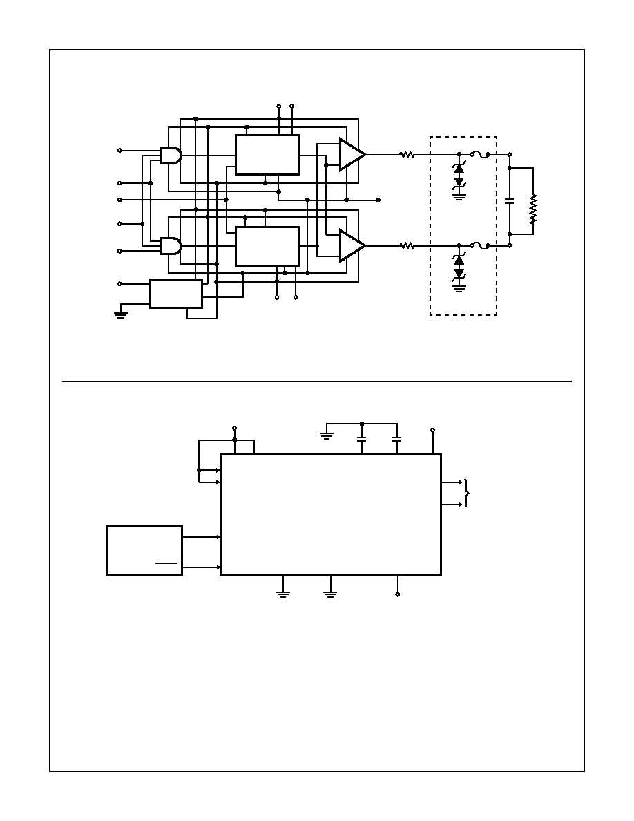
Block Diagram
Typical Application
NOTE: The rise and fall time of the outputs are set to ARINC specified values by C
A
and C
B
. Typical C
A
= C
B
= 75pF for high speed and
300pF for low speed operation. The output HI and low levels are set to ARINC specifications by V
REF
.
LEVEL SHIFTER
AND SLOPE
CONTROL (A)
LEVEL SHIFTER
AND SLOPE
CONTROL (B)
CURRENT
REGULATOR
DATA (A)
CLOCK
V
REF
SYNC
DATA (B)
V
1
(4)
(14)
(1)
(3)
(13)
(16)
(2)
(9) (5)
+V C
A
OUTPUT
DRIVER
(A)
R
OUT/2
R
OUT/2
OUTPUT
DRIVER
(B)
GND
(8)
-V
C
B
(7)
(12)
OVER-VOLTAGE
PROTECTION
F
A
F
B
C
L
A
OUT
B
OUT
R
L
(6)
(11)
HS-3182
ARINC DRIVER
CIRCUIT
16 LEAD DIP
GND
GND
-V
DATA (B)
DATA (A)
SYNC
CLOCK
V
1
V
REF
C
A
C
B
+V
A
OUT
B
OUT
TO BUS
(SEE
NOTE)
PIN NUMBER 10, 15 = NC
-15V
(7)
(8)
(2)
(9)
+15V
C
A
C
B
(12)
(5)
+5V
(1)
(16)
(14)
(3)
PIN NUMBERS INDICATED BY ( )
HS-3282
CMOS ARINC
CIRCUIT
429D0
429D0
31
32
(4)
(13)
HS-3182
5-180
Absolute Maximum Ratings
Thermal Information
Voltage Between +V and -V Terminals . . . . . . . . . . . . . . . . . . . . 40V
V
1
. . . . . . . . . . . . . . . . . . . . . . . . . . . . . . . . . . . . . . . . . . . . . . . . . 7V
V
REF
. . . . . . . . . . . . . . . . . . . . . . . . . . . . . . . . . . . . . . . . . . . . . . . 6V
Logic Input Voltage . . . . . . . . . . . . . . . . . . . . GND -0.3V to V
1
+0.3V
ESD Classification . . . . . . . . . . . . . . . . . . . . . . . . . . . . . . . . Class 1
Output Short Circuit Duration . . . . . . . . . . . . . . . . . . . . . See Note 1
Output Over-Voltage Protection . . . . . . . . . . . . . . . . . . . See Note 2
Recommended Operating Conditions
Operating Voltage
+V . . . . . . . . . . . . . . . . . . . . . . . . . . . . . . . . . . . . . . . .+15V
±
10%
-V . . . . . . . . . . . . . . . . . . . . . . . . . . . . . . . . . . . . . . . . -15V
±
10%
V
1
. . . . . . . . . . . . . . . . . . . . . . . . . . . . . . . . . . . . . . . . . . .5V
±
5%
V
REF
(For ARINC 429) . . . . . . . . . . . . . . . . . . . . . . . . . . .5V
±
5%
Operating Temperature Range
HS-3182-5. . . . . . . . . . . . . . . . . . . . . . . . . . . . . . . . 0
o
C to +70
o
C
HS-3182-8. . . . . . . . . . . . . . . . . . . . . . . . . . . . . . -55
o
C to +125
o
C
Thermal Resistance (Typical)
JA
JC
SBDIP Package . . . . . . . . . . . . . . . . . .
75
o
C/W
18
o
C/W
CLCC Package . . . . . . . . . . . . . . . . . .
60
o
C/W
14
o
C/W
Storage Temperature Range . . . . . . . . . . . . . . . . . .-65
o
C to +150
o
C
Maximum Junction Temperature . . . . . . . . . . . . . . . . . . . . . . +175
o
C
Maximum Lead Temperature (Soldering 10s) . . . . . . . . . . . . +300
o
C
Die Characteristics
Transistor Count . . . . . . . . . . . . . . . . . . . . . . . . . . . . . . . . . . . . . 133
NOTES:
1. Heat sink may be required for 100K bits/s at +125
o
C and output short circuit at +125
o
C.
2. The fuses used for output over-voltage protection may be blown by a fault at each output of greater than
±
6.5V relative to GND.
CAUTION: Stresses above those listed in "Absolute Maximum Ratings" may cause permanent damage to the device. This is a stress only rating and operation
of the device at these or any other conditions above those indicated in the operational sections of this specification is not implied.
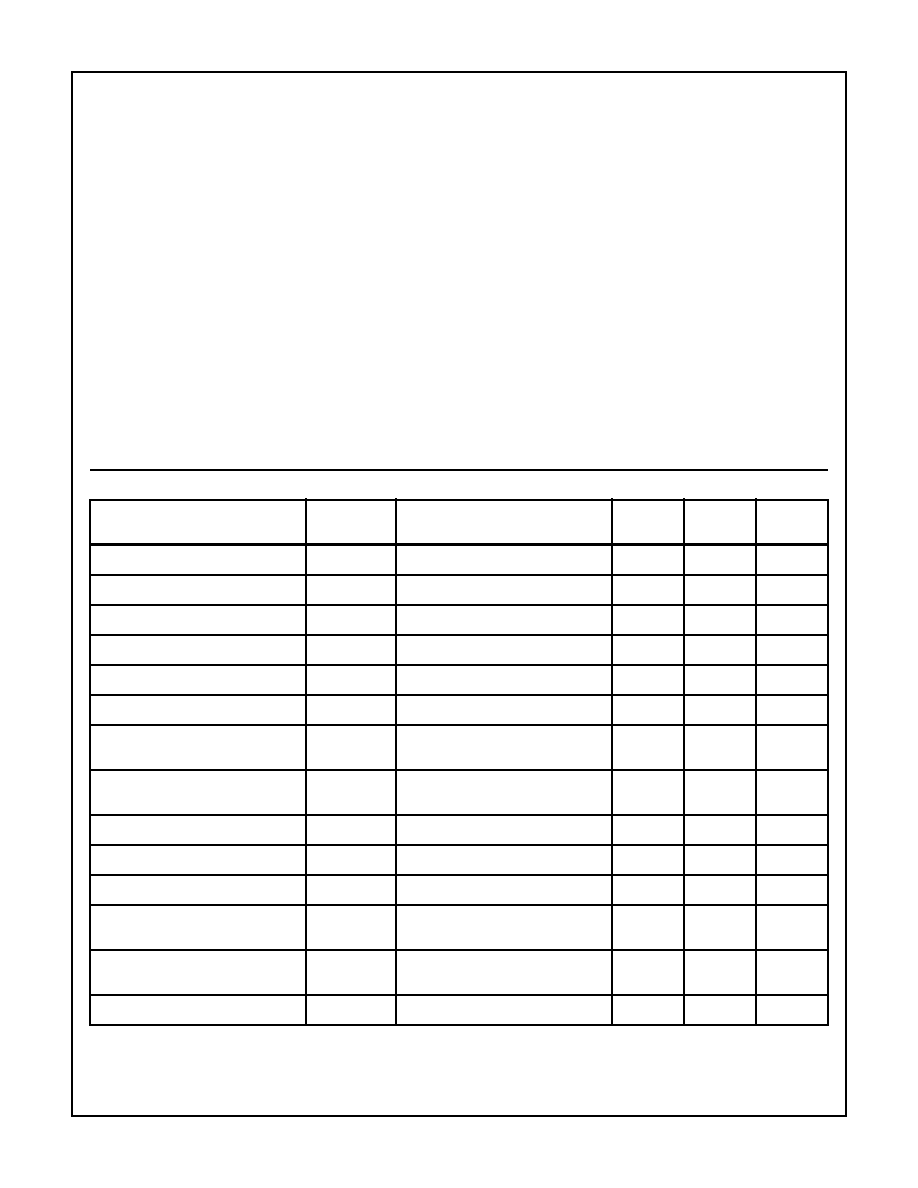
DC Electrical Performance Specifications
DC PARAMETER
SYMBOL
(NOTE 1)
CONDITIONS
MIN
MAX
UNITS
Supply Current +V (Operating)
I
CCOP
(+V)
No Load (0-100K bits/s)
-
16
mA
Supply Current -V (Operating)
I
CCOP
(-V)
No Load (0-100K bits/s)
-16
-
mA
Supply Current V
1
(Operating)
I
CCOP
(V
1
)
No Load (0-100K bits/s)
-
975
µ
A
Supply Current V
REF
(Operating)
I
CCOP
(V
REF
)
No Load (0-100K bits/s)
-1.0
-
mA
Logic "1" Input Voltage
V
IH
2.0
-
V
Logic "0" Input Voltage
V
IL
-
0.5
V
Output Voltage High (Output to GND)
V
OH
No Load (0-100K bits/s)
V
REF
(-250mV)
V
REF
(+250mV)
Output Voltage Low (Output to GND)
V
OL
No Load (0-100K bits/s)
-V
REF
(-250mV)
-V
REF
(+250mV)
Output Voltage Null
V
NULL
No Load (0-100K bits/s)
-250
+250
mV
Input Current (Input Low)
I
IL
-20
-
µ
A
Input Current (Input High)
I
IH
-
10
µ
A
Output Short Circuit Current
(Output High)
I
OHSC
Short to GND
-
-80
mA
Output Short Circuit Current
(Output Low)
I
OLSC
Short to GND
80
-
mA
Output Impedance
Z
O
T
A
= +25
o
C
60
90
NOTE:
1. +V = +15V
±
10%, -V = -15V
±
10%, V
1
= V
REF
= 5V
±
5%, unless otherwise specified T
A
= 0
o
C to +70
o
C for HS-3182-5 and
T
A
= -55
o
C to +125
o
C for HS-3182-8.
HS-3182

5-181
AC Electrical Performance Specifications
AC PARAMETER
SYMBOL
(NOTE 1)
CONDITIONS
MIN
MAX
UNITS
Rise Time (A
OUT
, B
OUT
)
t
R
C
A
= C
B
= 75pF, Note 2
1
2
µ
S
(at T
A
= -55
o
C Only)
0.9
2.4
µ
S
C
A
= C
B
= 300pF, Note 2
3
9
µ
S
Fall Time (A
OUT
, B
OUT
)
t
F
C
A
= C
B
= 75pF, Note 3
1
2
µ
S
(at T
A
= -55
o
C Only)
0.9
2.4
µ
S
C
A
= C
B
= 300pF, Note 3
3
9
µ
S
Propagation Delay Input to Output
t
PLH
C
A
= C
B
= 75pF, No Load
-
3.3
µ
S
Propagation Delay Input to Output
t
PHL
C
A
= C
B
= 75pF, No Load
-
3.3
µ
S
NOTES:
1. +V = +15V, -V = -15V, V
1
= V
REF
= 5V, unless otherwise specified T
A
= 0
o
C to +70
o
C for HS-3182-5 and T
A
= -55
o
C to +125
o
C for
HS-3182-8.
2. t
R
measured 50% to 90% times 2, no load.
3. t
F
measured 50% to 10% times 2, no load.
Electrical Performance Specifications
PARAMETER
SYMBOL
(NOTE 1)
CONDITIONS
MIN
MAX
UNITS
Input Capacitance
C
IN
T
A
= +25
o
C
-
15
pF
Supply Current +V (Short Circuit)
I
SC
(+V)
Short to GND, T
A
= +25
o
C
-
150
mA
Supply Current -V (Short Circuit)
I
SC
(-V)
Short to GND, T
A
= +25
o
C
-150
-
mA
NOTE:
1. The parameters listed in Table 3 are controlled via design or process parameters and are not directly tested. These parameters are char-
acterized upon initial design and after major process and/or design changes affecting these parameters.
Power Specifications
Nominal Power at +25
o
C, +V = +15V, -V = -15V, V1 = V
REF
= 5V, Notes 1, 3
DATA RATE
(K BITS/s)
LOAD
+V
V-
V
1
CHIP POWER
POWER DISSIPATION
IN LOAD
0-100
No Load
11mA
-10mA
600
µ
A
325mW
0
12.5-14
Full Load, Note 2
24mW
-24mW
600
µ
A
660mW
60mW
100
Full Load, Note 2
46mW
-46mW
600
µ
A
1 Watt
325mW
NOTES:
1. Heat sink may be required for 100K bits/s at +125
o
C and output short circuit at +125
o
C.
Thermal characteristics: T
(CASE)
= T
(Junction)
-
(Junction - Case)
P
(Dissipation)
.
Where: T
(Junction Max)
= +175
o
C
(Junction - Case)
= 10.9
o
C/W (6.1
o
C/W for LCC)
(Junction - Ambient)
= 73.5
o
C/W (54.0
o
C/W for LCC)
2. Full Load for ARINC 429: R
L
= 400
and C
L
= 30,000pF in parallel between A
OUT
and B
OUT
(see block diagram).
3. Output Over-Voltage Protection: The fuses used for output over-voltage protection may be blown by a fault at each output of greater than
±
6.5V relative to GND.
HS-3182
5-182
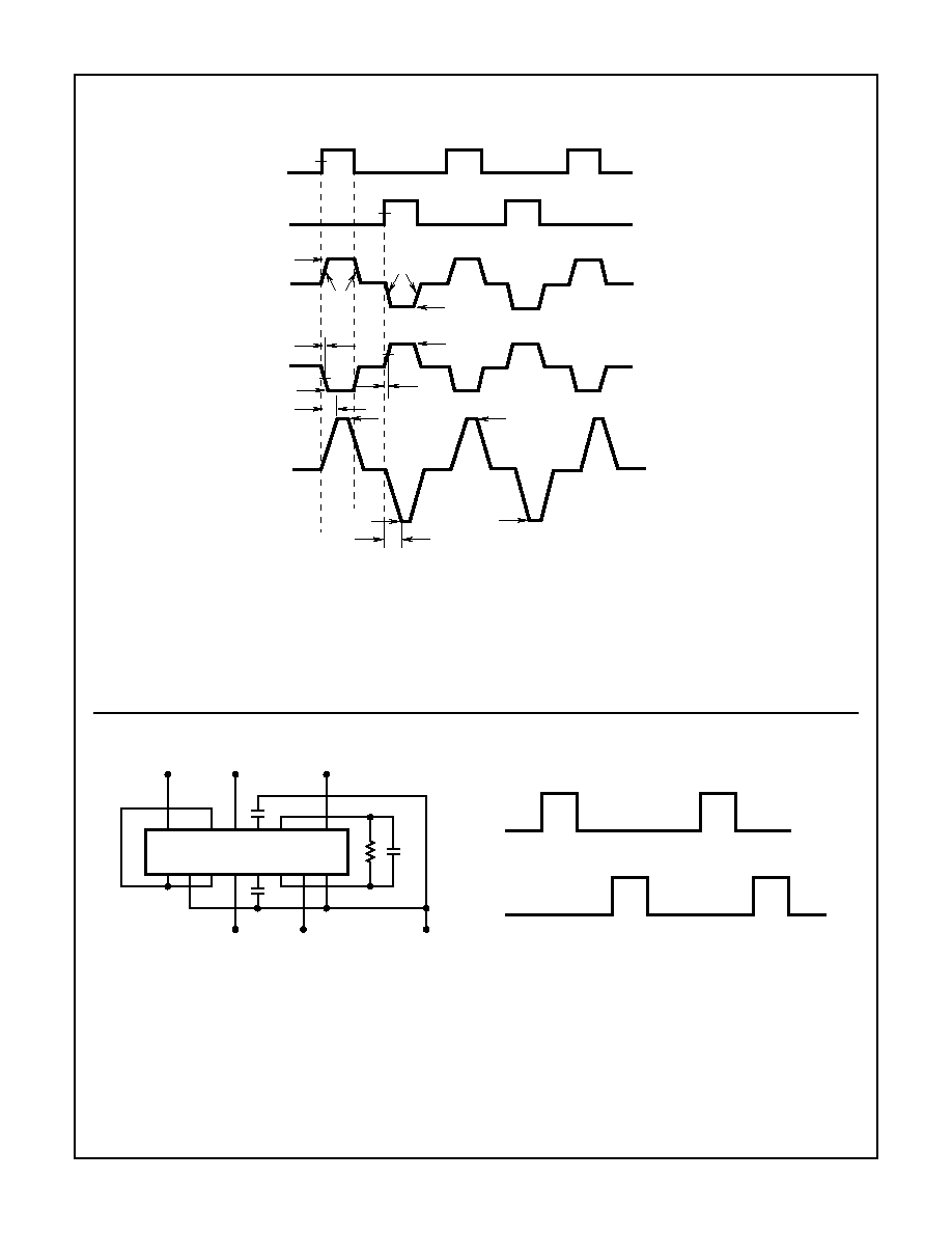
Driver Waveforms
NOTES: t
R
measured 50% to 90% times 2
t
F
measured 50% to 10% times 2
V
IH
= 5V
V
OL
= -4.75V to -5.25V
V
IL
= 0V
V
OH
= 4.75V to 5.25V
When the Data (A) input is in the Logic One state and the Data (B)
input is in the Logic Zero state, A
OUT
is equal to V
REF
and B
OUT
is
equal to -V
REF
. This constitutes the Output High state. Data (A) and
Data (B) both in the Logic Zero state causes both A
OUT
and B
OUT
to
be equal to 0V which designates the output Null state. Data (A) in
the Logic Zero state and Data (B) in the Logic One state causes
A
OUT
to be equal to -V
REF
and B
OUT
to be equal to V
REF
which is
the Output Low state.
Burn-In Schematic
NOTES: R = 400
±
5%
C
1
= 0.03
µ
F
±
20%
C
2
= C
3
= 500pF, NPO
+V = +15.5V
±
0.5V
-V = -15.5V
±
0.5V
V
1
= +5.5V
±
0.5V
A 0.0
µ
F decoupling capacitor is required on each of the three
supply lines (+V, -V and V
1
) at every 3rd Burn-In socket.
Ambient Temp. Max. = +125
o
C.
Package = 16 Lead Side Brazed DIP.
Pulse Conditions = A & B = 6.25kHz
±
10%. B is delayed one-half
cycle and in sync with A.
V
IH
= 2.0V Min.
V
IL
= 0.5V Max.
DATA (A) 0V
DATA (B) 0V
V
REF
A
OUT
0V
B
OUT
0V
t
PHL
-V
REF
A
OUT
- B
OUT
0V
DIFFERENTIAL
OUTPUT
50%
50%
50%
50%
t
PLH
t
R
t
F
2V
REF
-V
REF
V
REF
HIGH
NULL
LOW
-2V
REF
ADJ. BY
C
B
ADJ. BY
C
A
5V
0V
5V
0V
+4.75V TO +5.25V
-4.75V TO -5.25V
+4.75V TO +5.25V
-4.75V TO -5.25V
+9.5V TO +10.5V
NOTE: OUTPUTS UNLOADED
-9.5V TO -10.5V
V
1
DATA (B)
+V
C
1
GND
-V
DATA (A)
16
15
14
13
12
11
10
9
1
2
3
4
5
6
7
8
C
3
C
2
R
HS-3182
V
IL
V
IH
V
IH
V
IL
A
B
HS-3182