
6-1
March 1997
HM-6642
512 x 8 CMOS PROM
Features
∑ Low Power Standby and Operating Power
- ICCSB . . . . . . . . . . . . . . . . . . . . . . . . . . . . . . . . .100
µ
A
- ICCOP . . . . . . . . . . . . . . . . . . . . . . . . . . 20mA at 1MHz
∑ Fast Access Time. . . . . . . . . . . . . . . . . . . . . . 120/200ns
∑ Industry Standard Pinout
∑ Single 5.0V Supply
∑ CMOS/TTL Compatible Inputs
∑ Field Programmable
∑ Synchronous Operation
∑ On-Chip Address Latches
∑ Separate Output Enable
Description
The HM-6642 is a 512 x 8 CMOS NiCr fusible link
Programmable Read Only Memory in the popular 24 pin,
byte wide pinout. Synchronous circuit design techniques
combine with CMOS processing to give this device high
speed performance with very low power dissipation.
On-chip address latches are provided, allowing easy
interfacing with recent generation microprocessors that use
multiplexed address/data bus structures, such as the 8085.
The output enable controls, both active low and active high,
further simplify microprocessor system interfacing by
allowing output data bus control independent of the chip
enable control. The data output latches allow the use of the
HM-6642 in high speed pipelined architecture systems, and
also in synchronous logic replacement functions.
Applications for the HM-6642 CMOS PROM include low
power handheld microprocessor based instrumentation and
communications systems, remote data acquisition and
processing systems, processor control store, and synchro-
nous logic replacement.
All bits are manufactured storing a logical "0" and can be
selectively programmed for a logical "1" at any bit location.
Ordering Information
PACKAGE
TEMPERATURE RANGE
120ns
200ns
PKG. NO.
SBDIP
-40
o
C to +85
o
C
HM1-6642B-9
HM1-6642-9
D24.6
SMD#
-55
o
C to +125
o
C
5962-8869002JA
5962-8869001JA
D24.6
SLIM SBDIP
-40
o
C to +85
o
C
HM6-6642B-9
HM6-6642-9
D24.3
SMD#
-55
o
C to +125
o
C
5962-8869002LA
5962-8869001LA
D24.3
CLCC
-40
o
C to +85
o
C
-
HM4-6642-9
J28.A
SMD#
-55
o
C to +125
o
C
5962-88690023A
5962-88690013A
J28.A
File Number
3012.1
CAUTION: These devices are sensitive to electrostatic discharge; follow proper IC Handling Procedures.
http://www.intersil.com or 407-727-9207
|
Copyright
©
Intersil Corporation 1999

6-3
Programming
Introduction
The HM-6642 is a 512 word by 8-bit field Programmable
Read Only Memory utilizing nicrome fusible links as pro-
grammable memory elements. Selected memory locations
are permanently changed from their manufactured state, of
all low (V
OL
) to a logical high (V
OH
), by the controlled
application of programming potentials and pulses. Careful
adherence to the following programming specifications will
result in high programming yield. Both high V
CC
(6.0V) and
low V
CC
(4.0V) verify cycles are specified to assure the
integrity of the programmed fuse. This programming
specification, although complete, does not preclude rapid
programming. The worst case programming time required is
37.4 seconds, and typical programming time can be
approximately 4 seconds per device.
The chip (E) and output enable (G) are used during the
programming procedure. On PROMs which have more than
one output enable control G3 is to be used. The other output
enables must be held in the active, or enabled, state
throughout the entire programming sequence. The program-
mer designer is advised that all pins of the programmer's
socket should be at ground potential when the PROM is
inserted into the socket. V
CC
must be applied to the PROM
before any input or output pin is allowed to rise (See Note).
Overall Programming Procedure
1. The address of the first bit to be programmed is
presented, and latched by the chip enable (E) falling
edge. The output is disabled by taking the output enable
G Low: The programming pin is enabled by taking (P)
high.
2. V
CC
is raised to the programming voltage level, 12.5V.
3. All data output pins are pulled up to V
CC
program. Then
the data output pin corresponding to the bit to be
programmed is pulled low for 100ms. Only one bit should
be programmed at a time.
4. The data output pin is returned to V
CC
, and the V
CC
pin
is returned to 6.0V.
5. The address of the bit is again presented, and latched by
a second chip enable falling edge.
6. The data outputs are enabled, and read, to verify that the
bit was successfully programmed.
a). If verified, the next bit to be programmed is addressed
and programmed.
b). If not verified, the programs verify sequence is
repeated up to 8 times total.
7. After all bits to be programmed have been verified at 6.0V,
the V
CC
is lowered to 4.0V and all bits are verified.
a). If all bits verify, the device is properly programmed.
b). If any bit fails to verify, the device is rejected.
Programming System Requirements
1. The power supply for the device to be programmed must
be able to be set to three voltages: 4.0V, 6.0V, 12.5V. This
supply must be able to supply 500mA average, and 1A
dynamic, currents to the PROM during programming. The
power supply rise fall times when switching between volt-
ages must be no quicker than 1ms.
2. The address drivers must be able to supply a V
IH
of 4.0V
and 6.0V and V
IL
when the system is at programming
voltages. (See Note)
3. The control input buffers must be able to maintain input
voltage levels of
70% and
20% V
CC
for V
IH
and V
IL
levels, respectively. Notice that chip enable (E) and G
does not require a pull up to programming voltage levels.
The program control (P) must switch from ground to VIH
and from V
IH
to the V
CC
PGM level. (See Note)
4. The data input buffers must be able to sink up to 3mA
from the PROM's output pins without rising more than
0.7V above ground, be able to hold the other outputs high
with a current source capability of 0.5mA to 2.0mA, and
not interfere with the reading and verifying of the data
output of the PROM. Notice that a bit to be programmed
is changed from a low state (V
OL
) to high (V
OH
) by pulling
low on the output pin. A suggested implementation is
open collector TTL buffers (or inverters) with 4.7k
pull
up resistors to V
CC
. (See Note)
NOTE: Never allow any input or output pin to rise more than 0.3V
above V
CC
, or fall more than 0.3V below ground.
HM-6642
6-4
Background Information HM-6642 Programming
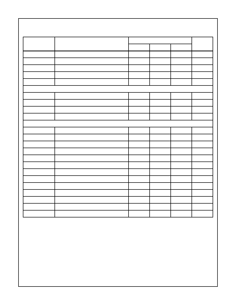
PROGRAMMING SPECIFICATIONS
SYMBOL
PARAMETER
LIMITS
UNITS
MIN
TYP
MAX
VCC PROG
Programming VCC
12.0
12.0
12.5
V
VCCN
Operating VCC
4.5
5.5
5.5
V
VCC LV
Special Verify VCC
4.0
-
6.0
V
ICC
System ICC Capability
500
-
-
mA
ICC Peak
Transient ICC Capability
1.0
-
-
A
PROM INPUT PINS
VOL
Output Low Voltage (To PROM)
-0.3
GND
20% VCC
V
VOH
Output High Voltage (To PROM)
70% VCC
VCC
VCC +0.3
V
IOL
Output Sink Current (At VOL)
0.01
-
-
mA
IOH
Output Source Current (At VOH)
0.01
-
-
mA
PROM DATA OUTPUT PINS
VOL
Output Low Voltage (To PROM)
-0.3
GND
0.7
V
VOH
Output High Voltage (To PROM)
70% VCC
VCC
VCC +0.3
V
IOL
Output Sink Current (At VOL)
3.0
-
-
mA
IOH
Output Source Current (At VOH)
0.5
1.0
2.0
mA
tD
Delay Time
1.0
1.0
-
µ
s
tR
Rise Time
1.0
10.0
10.0
µ
s
tF
Fall Time
1.0
10.0
10.0
µ
s
TEHEL
Chip Enable Pulse Width
500
-
-
ns
TAVEL
Address Valid to Chip Enable Low Time
500
-
-
ns
TELQV
Chip Enable Low to Output Valid Time
-
-
500
ns
tpw
Programming Pulse Width
90
100
110
µ
s
tIP
Input Leakage at VCC = VCC PROG
-10
+1.0
10
µ
A
TA
Ambient Temperature
-
25
-
o
C
HM-6642

