
1
File Number
3543.3
HS-0548RH, HS-0549RH
Radiation Hardened Single 8/Differential 4
Channel CMOS Analog Multiplexers with
Active Overvoltage Protection
The HS-0548RH and HS-0549RH are radiation hardened
analog multiplexers with Active Overvoltage Protection and
guaranteed r
ON
matching. Analog input levels may greatly
exceed either power supply without damaging the device or
disturbing the signal path of other channels. Active
protection circuitry assures that signal fidelity is maintained
even under fault conditions that would destroy other
multiplexers. Analog inputs can withstand constant 70V
peak-to-peak levels with
±
15V supplies and digital inputs will
sustain continuous faults up to 4V greater than either supply.
In addition, signal sources are protected from short circuiting
should multiplexer supply loss occur: each input presents
1k
of resistance under this condition. These features make
the HS-0548RH and HS-0549RH ideal for use in systems
where the analog inputs originate from external equipment
or separately powered circuitry. Both devices are fabricated
with 44V dielectrically isolated CMOS technology. The
HS-0548 is an 8 channel device and the HS-0549 is a
4 channel differential version. If input overvoltage protection
is not needed, the HS-0508 and HS-509 multiplexers are
recommended.
Specifications for Rad Hard QML devices are controlled
by the Defense Supply Center in Columbus (DSCC). The
SMD numbers listed here must be used when ordering.
Detailed Electrical Specifications for these devices are
contained in SMD 5962-95694. A "hot-link" is provided
on our homepage for downloading.
http://www.intersil.com/spacedefense/space.htm
Features
∑ Electrically Screened to SMD # 5962-95694
∑ QML Qualified per MIL-PRF-38535 Requirements
∑ Gamma Dose . . . . . . . . . . . . . . . . . . . . . . 1 x 10
4
RAD(Si)
∑ No Latch-Up
∑ No Channel Interaction During Overvoltage
∑ Guaranteed r
ON
Matching
∑ Maximum Power Supply . . . . . . . . . . . . . . . . . . . . . . . 44V
∑ Break-Before-Make Switching
∑ Analog Signal Range . . . . . . . . . . . . . . . . . . . . . . . .
±
15V
∑ Access Time. . . . . . . . . . . . . . . . . . . . . . . . . . . . . . . 1.0
µ
s
Applications
∑ Data Acquisition Systems
∑ Control Systems
∑ Telemetry
Pinouts
HS-0548RH GDIP1-T16 (CERDIP)
OR CDIP2-T16 (SBDIP)
TOP VIEW
HS-0549RH GDIP1-T16 (CERDIP)
OR CDIP2-T16 (SBDIP)
TOP VIEW
Ordering Information
ORDERING NUMBER
INTERNAL
MKT. NUMBER
TEMP. RANGE
(
o
C)
5962D9569401VEA
HS1-0548RH-Q
-55 to 125
5962D9569401VEC
HS1B-0548RH-Q
-55 to 125
5962D9569402VEA
HS1-0549RH-Q
-55 to 125
5962D9569402VEC
HS1B-0549RH-Q
-55 to 125
14
15
16
9
13
12
11
10
1
2
3
4
5
7
6
8
AO
ENABLE
-V
SUPPLY
IN 1
IN 2
IN 3
OUT
IN 4
A1
GND
+V
SUPPLY
IN 5
IN 6
IN 7
IN 8
A2
14
15
16
9
13
12
11
10
1
2
3
4
5
7
6
8
A0
ENABLE
-V
SUPPLY
IN 1A
IN 2A
IN 3A
OUTA
IN 4A
A1
+V
SUPPLY
IN 1B
IN 2B
IN 3B
IN 4B
OUT B
GND
Data Sheet
August 1999
CAUTION: These devices are sensitive to electrostatic discharge; follow proper IC Handling Procedures.
http://www.intersil.com or 407-727-9207
|
Copyright
©
Intersil Corporation 1999

4
FIGURE 5. ADDRESS DECODER
FIGURE 6. MULTIPLEX SWITCH
Schematic Diagrams
(Continued)
+V
ENABLE
P
P
P
P
P
P
N
N
N
N
N
N
A0 OR A0
A1 OR A1
A2 OR A2
TO P-CHANNEL DEVICE OF THE SWITCH PAIR
TO N-CHANNEL DEVICE OF THE SWITCH PAIR
V-
D
6
D
7
D
4
D
5
V
OUT
IN
R
11
1K
FROM
DECODE
FROM
DECODE
OVERVOLTAGE
PROTECTION
V+
Q
6
N
N
N
Q
5
P
P
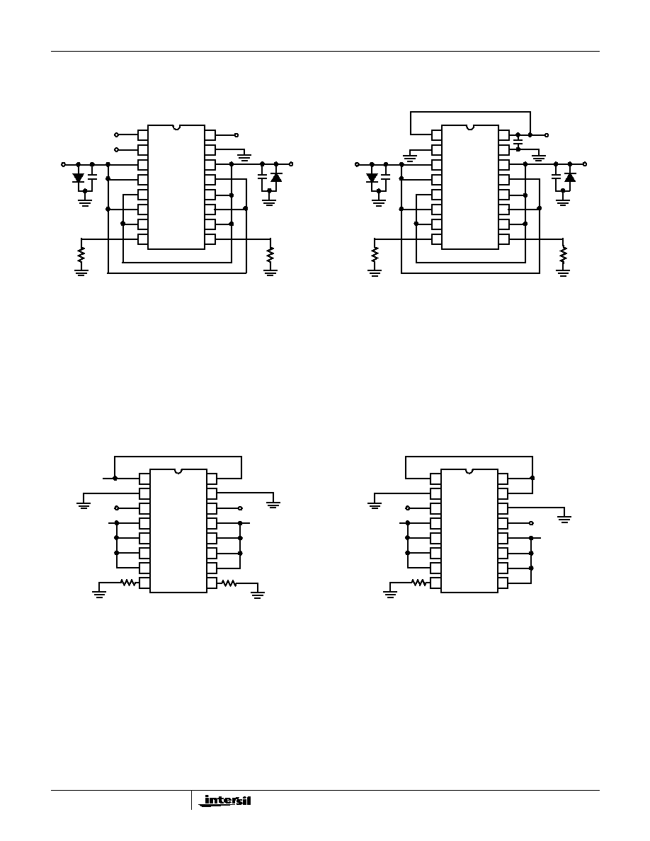
Burn-In/Life Test Circuits
HS-0548RH
DYNAMIC BURN-IN AND LIFE TEST CIRCUIT
V
1
= -15V maximum, -16V minimum
V
2
= +15V minimum, +16V maximum
R
1
= 10k
±
5% 1/4W
C
1
= C
2
= 0.01
µ
F minimum (per socket) or 0.1
µ
F minimum
(per row)
D
1
= D
2
= 1N4002 (or equivalent)
F
0
= 100kHz 50% duty cycle; V
IL
= 0.8V Max; V
IH
= 4.0V Min.
F
1
= F
0/2
F
2
= F
1/2
F
3
= F
2/2
HS-0548RH
STATIC BURN-IN TEST CIRCUIT
V
1
= 5V minimum, 6V maximum
V
2
= -15V maximum, -16V minimum
V
3
= +15V minimum, +16V maximum
R
1
= 10k
±
5% 1/4W
C
1
= C
2
= 0.01
µ
F minimum (per socket) or 0.1
µ
F minimum
(per row)
D
1
= D
2
= 1N4002 (or equivalent)
14
15
16
9
13
12
11
10
1
2
3
4
5
7
6
8
F
0
F
3
V
1
D
1
C
1
R
1
F
1
F
2
V
2
D
2
C
2
14
15
16
9
13
12
11
10
1
2
3
4
5
7
6
8
V
2
D
1
C
1
R
1
V
1
V
3
D
2
C
2
HS-0548RH, HS-0549RH
5
HS-0549RH
DYNAMIC BURN-IN AND LIFE TEST CIRCUIT
V
2
= +15.5V,
±
.0.5V
V
3
= -15.5V,
±
0.5V
R
1
= 10k
,
±
5%
C
1
= 0.01
µ
F minimum (per socket)
D
1
= 1N4002 or equivalent (per board)
F
0
= 100kHz,
±
10%; F
1
= F
0/2
; F
2
= F
1/2
,
50% duty cycle, V
IL
= 0.8V Max; V
IH
= 4.0V Min
HS-0549RH
STATIC BURN-IN TEST CIRCUIT
V
1
= +5.5V,
±
0.5V
V
2
= +15.5V,
±
0.5V
V
3
= -15.5V,
±
0.5V
R
1
= 10k
,
±
10%
C
1
= 0.01
µ
F minimum (per socket)
D
1
= 1N4002 or equivalent (per board)
Burn-In/Life Test Circuits
(Continued)
14
15
16
9
13
12
11
10
1
2
3
4
5
7
6
8
F
0
F
2
V
2
V
3
D
1
C
1
R
1
R
1
D
1
C
1
F
1
14
15
16
9
13
12
11
10
1
2
3
4
5
7
6
8
V
2
V
3
D
1
C
1
R
1
R
1
D
1
C
1
V
1
Irradiation Circuits
HS-0549RH
R
1
= R
2
= 10k
±
5%
HS-0548RH
R
1
= 10k
±
5%
14
15
16
9
13
12
11
10
1
2
3
4
5
7
6
8
+5V
-15V
+1V
R
1
R
2
+1V
+15V
14
15
16
9
13
12
11
10
1
2
3
4
5
7
6
8
+5V
-15V
+1V
R
1
+1V
+15V
HS-0548RH, HS-0549RH

