
1
File Number
3961.3
HS-RTX2010RH
Radiation Hardened Real Time ExpressTM
Microcontroller
The HS-RTX2010RH is a radiation-hardened 16-bit
microcontroller with on-chip timers, an interrupt controller, a
multiply-accumulator, and a barrel shifter. It is particularly
well suited for space craft environments where very high
speed control tasks which require arithmetically intensive
calculations, including floating point math to be performed in
hostile space radiation environments.
This processor incorporates two 256-word stacks with
multitasking capabilities, including configurable stack
partitioning and over/underflow control.
Instruction execution times of one or two machine cycles are
achieved by utilizing a stack oriented, multiple bus
architecture. The high performance ASIC Bus, which is
unique to the RTX product, provides for extension of the
microcontroller architecture using off-chip hardware and
application specific I/O devices.
RTX Microcontrollers support the C and Forth programming
languages. The advantages of this product are further
enhanced through third party hardware and software support.
Combined, these features make the HS-RTX2010RH an
extremely powerful processor serving numerous
applications in high performance space systems. The
HS-RTX2010RH has been designed for harsh space
radiation environments and features outstanding Single
Event Upset (SEU) resistance and excellent total dose
response.
Specifications for Rad Hard QML devices are controlled
by the Defense Supply Center in Columbus (DSCC). The
SMD numbers listed here must be used when ordering.
Detailed Electrical Specifications for these devices are
contained in SMD 5962-95635. A "hot-link" is provided
on our homepage for downloading.
www.intersil.com/spacedefense/space.asp
Features
� Electrically Screened to SMD # 5962-95635
� QML Qualified per MIL-PRF-38535 Requirements
� Fast 125ns Machine Cycle
� 1.2
�
M TSOS4 CMOS/SOS Process
� Total Dose Capability . . . . . . . . . . . . . . . . . . 300KRad(Si)
� Single Event Upset Critical LET . . . . . . . >120MeV/mg/cm
2
� Single Event Upset Error Rate . . . . <1 x 10
-10
Errors/Bit-Day
(Note)
� -55
o
C - 125
o
C, 5V
�
10% Operation
� Single Cycle Instruction Execution
� Fast Arithmetic Operations
- Single Cycle 16-Bit Multiply
- Single Cycle 16-Bit Multiply Accumulate
- Single Cycle 32-Bit Barrel Shift
- Hardware Floating Point Support
� C Software Development Environment
� Direct Execution of Fourth Language
� Single Cycle Subroutine Call/Return
� Four Cycle Interrupt Latency
� On-Chip Interrupt Controller
� Three On-Chip 16-Bit Timer/Counters
� Two On-Chip 256 Word Stacks
� ASIC BusTM for Off-Chip Architecture Extension
� 1 Megabyte Total Address Space
� Word and Byte Memory Access
� Fully Static Design - DC to 8MHz Operation
� 84 Lead Quad Flat Package or 85 Pin Grid Array
� Third Party Software and Hardware Development Systems
NOTE: Single Event Upset error rates are Adams 10% worst case
environment under worst case conditions for upset.
Applications
� Space Systems Embedded Control
� Digital Filtering
� Image Processing
� Scientific Instrumentation
� Optical Systems
� Control Systems
� Attitude/Orbital Control
Ordering Information
ORDERING NUMBER
INTERNAL
MKT. NUMBER
TEMP. RANGE
(
o
C)
5962F9563501QXC
HS8-RTX2010RH-8
55 to 125
5962F9563501QYC
HS9-RTX2010RH-8
55 to 125
5962F9563501V9A
HS0-RTX2010RH-Q
25
5962F9563501VXC
HS8-RTX2010RH-Q
55 to 125
5962F9563501VYC
HS9-RTX2010RH-Q
55 to 125
HS8-RTX2010RH/Proto HS8-RTX2010RH/Proto
55 to 125
HS9-RTX2010RH/Proto HS9-RTX2010RH/Proto
55 to 125
Data Sheet
March 2000
CAUTION: These devices are sensitive to electrostatic discharge; follow proper IC Handling Procedures.
1-888-INTERSIL or 321-724-7143
|
Copyright
�
Intersil Corporation 2000
Real Time ExpressTM, RTXTM, and ASIC BusTM are trademarks of Intersil Corporation.

2
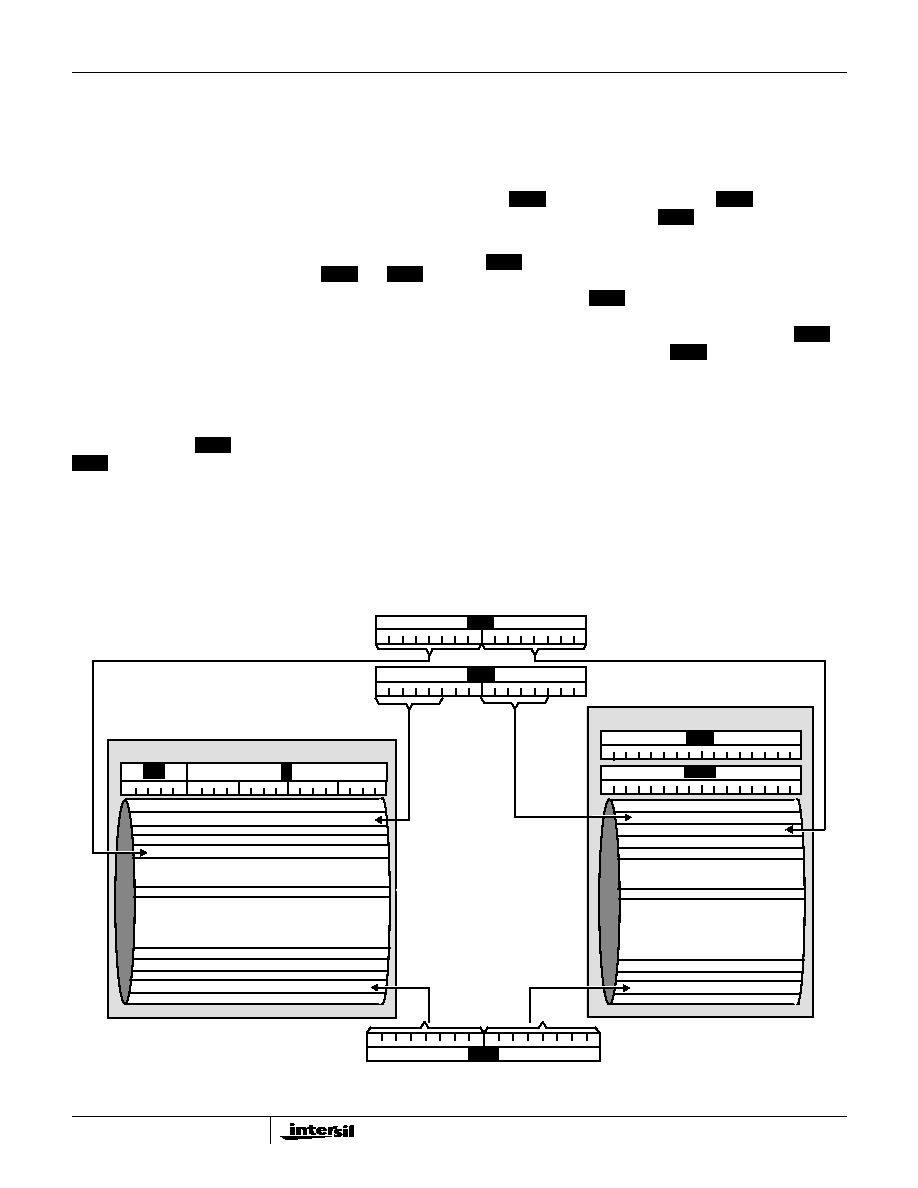
Block Diagram
HS-RTX2010RH
INPUTS
CONTROL
CLOCK AND
CONFIGURATION
CONTROL
MAIN
MEMORY
OFF CHIP
PERIPHERALS
INTERRUPT
INPUTS
INTERRUPT
CONTROL
TIMER
INPUTS
ASIC BUS
INTERFACE
MEMORY BUS
INTERFACE
PROCESSOR
RTX CORE
STACK
CONTROLLERS
BARREL
SHIFTER
MAC
RETURN
STACK
256-WORD
PARAMETER
STACK
256-WORD
MEMORY
PAGE
CONTROL
TIMER/
COUNTERS
Pinouts
HS8-RTX2010RH
MIL-STD-1835 CMGA3-P85C
NOTE: An overbar on a signal name represents an active LOW signal.
B
A
C
D
E
F
G
H
J
K
L
GA00
MD14
MD12
MD11
MD08
INTA
TCLK
E I5
GD15
MD05
GND
GND
MD04
MD03
MD02
GD07
MD00
NEW
MD01
VDD
LDS
UDS
GND
MA18
GND
MA04
MA08
GD05
MA10
MA13
MA15
MA17
MA19
MA05
MA07
GD04
MA09
MA12
VDD
MA14
MA16
MA06
MA11
GND
GD09
BOOT
PCLK
GD01 MA01
GA01
VDD
MD06
GA02
ICLK
MD15
MD13
MD10
MD09
MD07
NMI
GND
A
B
C
D
E
F
G
H
J
K
L
VDD
MA02 MA03
E I1
E I2
GD14 GD11 GD10
E I4
E I3
WAIT
GD13 GD12
GD06 GD03 GD02 GD00
GD08
INT-
SUP
1
10
11
4
3
7
8
9
5
6
2
RESET
PIN
A1
GR/W
GIO
MR/W
HS-RTX2010RH
TOP VIEW
PINS DOWN
8
9
10
11
2
3
4
5
1
7
6
C
J
K
L
H
G
F
E
D
B
A
C
J
K
L
H
G
F
E
D
B
A
PIN
A1
BOTTOM VIEW
PINS UP
GA00
MD14
MD12
MD11
MD08
TCLK
GD15
MD05
GND
GD13
GD14
GND
MD04
MD03
MD02
GD12
GD11
GD07
MD00
NEW
MD01
GD06
VDD
LDS
GND
MA18
GND
GD03
MA04
MA08
GD05
MA10
MA13
MA17
MA19
GD02
GD01
MA02
MA05
MA07
GD04
MA16
GD08
GD10
GD09
BOOT
GA01
VDD
MD06
GA02
MD15
MD13
MD10
MD09
MD07
E I4
E I1
GND
ICLK
UDS PCLK
MA15
INTSUP NMI
WAIT RESET E I3
E I2
VDD
INTA
E I5
MA09
MA12
MA14
GD00
MA01
MA03
MA06
MA11
GND
VDD
MR/W
GR/W
GIO
ALIGN.
PIN
HS-RTX2010RH

3
HS9-RTX2010RH
(LEAD LENGTH NOT TO SCALE) SEE INTERSIL OUTLINE R84.A
Pinouts
(Continued)
NOTE: An overbar on a signal name represents an active LOW signal.
HS-RTX2010RH
TOP VIEW
65
66
67
68
69
70
71
72
73
74
54
55
56
57
58
59
60
61
62
64
63
MD02
MD03
MD04
GND
MD05
MD06
MD07
VDD
MD08
MA17
MA18
MA19
GND
LDS
UDS
NEW
BOOT
PCLK
MD00
MD01
75
76
77
78
79
80
81
82
83
84
1
2
3
4
5
6
7
8
9
10
11
25
26
27
28
29
30
31
32
12
13
14
18
19
20
21
22
23
24
15
16
17
53
52
51
50
33
49
48
47
46
45
44
43
42
41
40
39
38
37
36
35
34
EI5
MD09
MD10
MD11
MD12
MD13
MD14
GND
MD15
GA00
GA01
GA02
TCLK
INT
A
NMI
INTSUP
VDD
EI1
EI2
EI3
EI4
MA04
MA03
MA02
MA01
GD00
GD01
GD02
MA16
MA15
MA14
MA13
VDD
MA12
MA11
MA10
MA09
GND
MA08
MA07
MA06
MA05
RESET
WAIT
ICLK
GD14
GD13
GND
GD12
GD11
GD10
GD09
GD08
GD07
VDD
GD06
GD05
GD04
GD03
GND
GD15
GR/W
GIO
MR/W
PGA And CQFP
Pin/Signal Assignments
CQFP
PGA
PIN
SIGNAL
NAME
TYPE
1
C6
GA02
Output; Address Bus
2
A6
TCLK
Output
3
A5
INTA
Output
4
B5
NMI
Input
5
C5
INTSUP
Input
6
A4
VDD
Power
7
B4
EI1
Input
8
A3
EI2
Input
9
A2
EI3
Input
10
B3
EI4
Input
11
A1
EI5
Input
12
B2
RESET
Input
13
C2
WAIT
Input
14
B1
ICLK
Input
15
C1
GR/W
Output
16
D2
GIO
Output
17
D1
GD15
I/O; Data Bus
18
E3
GD14
I/O; Data Bus
19
E2
GD13
I/O; Data Bus
20
E1
GND
Ground
21
F2
GD12
I/O; Data Bus
22
F3
GD11
I/O; Data Bus
23
G3
GD10
I/O; Data Bus
24
G1
GD09
I/O; Data Bus
25
G2
GD08
I/O; Data Bus
26
F1
GD07
I/O; Data Bus
27
H1
VDD
Power
28
H2
GD06
I/O; Data Bus
29
J1
GD05
I/O; Data Bus
30
K1
GD04
I/O; Data Bus
31
J2
GD03
I/O; Data Bus
32
L1
GND
Ground
33
K2
GD02
I/O; Data Bus
34
K3
GD01
I/O; Data Bus
35
L2
GD00
I/O; Data Bus
36
L3
MA01
Output; Address Bus
37
K4
MA02
Output; Address Bus
38
L4
MA03
Output; Address Bus
39
J5
MA04
Output; Address Bus
40
K5
MA05
Output; Address Bus
41
L5
MA06
Output; Address Bus
42
K6
MA07
Output; Address Bus
43
J6
MA08
Output; Address Bus
44
J7
GND
Ground
45
L7
MA09
Output; Address Bus
46
K7
MA10
Output; Address Bus
PGA And CQFP
Pin/Signal Assignments
(Continued)
CQFP
PGA
PIN
SIGNAL
NAME
TYPE
HS-RTX2010RH

4
47
L6
MA11
Output; Address Bus
48
L8
MA12
Output; Address Bus
49
K8
MA13
Output; Address Bus
50
L9
VDD
Power
51
L10
MA14
Output; Address Bus
52
K9
MA15
Output; Address Bus
53
L11
MA16
Output; Address Bus
54
K10
MA17
Output; Address Bus
55
J10
MA18
Output; Address Bus
56
K11
MA19
Output; Address Bus
57
J11
GND
Ground
58
H10
LDS
Output
59
H11
UDS
Output
60
F10
NEW
Output
61
G10
BOOT
Output
62
G11
PCLK
Output
63
G9
MR/W
Output
64
F9
MD00
I/O; Data Bus
65
F11
MD01
I/O; Data Bus
PGA And CQFP
Pin/Signal Assignments
(Continued)
CQFP
PGA
PIN
SIGNAL
NAME
TYPE
66
E11
MD02
I/O; Data Bus
67
E10
MD03
I/O; Data Bus
68
E9
MD04
I/O; Data Bus
69
D11
GND
Ground
70
D10
MD05
I/O; Data Bus
71
C11
MD06
I/O; Data Bus
72
B11
MD07
I/O; Data Bus
73
C10
VDD
Power
74
A11
MD08
I/O; Data Bus
75
B10
MD09
I/O; Data Bus
76
B9
MD10
I/O; Data Bus
77
A10
MD11
I/O; Data Bus
78
A9
MD12
I/O; Data Bus
79
B8
MD13
I/O; Data Bus
80
A8
MD14
I/O; Data Bus
81
B6
GND
Ground
82
B7
MD15
I/O; Data Bus
83
A7
GA00
Output; Address Bus
84
C7
GA01
Output; Address Bus
-
C3
-
Isolated Alignment Pin
PGA And CQFP
Pin/Signal Assignments
(Continued)
CQFP
PGA
PIN
SIGNAL
NAME
TYPE
Output Signal Descriptions
SIGNAL
CQFP
RESET
LEVEL
DESCRIPTION
OUTPUTS
NEW
60
1
NEW: A HIGH on this pin indicates that an Instruction Fetch is in progress.
BOOT
61
1
BOOT: A HIGH on this pin indicates that Boot Memory is being accessed. This pin can be set or reset by accessing
bit 3 of the Configuration Register.
MR/W
63
1
MEMORY READ/WRITE: A LOW on this pin indicates that a Memory Write operation is in progress.
UDS
59
1
UPPER DATA SELECT: A HIGH on this pin indicates that the high byte of memory (MD15-MD08) is being
accessed.
LDS
58
1
LOWER DATA SELECT: A HIGH on this pin indicates that the low byte of memory (MD07-MD00) is being
accessed.
GIO
16
1
ASIC I/O: A LOW on this pin indicates that an ASIC Bus operation is in progress.
GR/W
15
1
ASIC READ/WRITE: A LOW on this pin indicates that an ASIC Bus Write operation is in progress.
PCLK
62
0
PROCESSOR CLOCK: Runs at half the frequency of ICLK. All processor cycles begin on the rising edge of PCLK.
Held low extra cycles when WAIT is asserted.
TCLK
2
0
TIMING CLOCK: Same frequency and phase as PCLK but continues running during Wait cycles.
INTA
3
0
INTERRUPT ACKNOWLEDGE: A HIGH on this pin indicates that an Interrupt Acknowledge cycle is in progress.
Input Signal, Bus, and Power Connection Descriptions
SIGNAL
CQFP
LEAD
DESCRIPTION
INPUTS
WAIT
13
WAIT: A HIGH on this pin causes PCLK to be held LOW and the current cycle to be extended.
ICLK
14
INPUT CLOCK: Internally divided by 2 to generate all on-chip timing (CMOS input levels).
RESET
12
A HIGH level on this pin resets the RTX. Must be held high for at least 4 rising edges of ICLK plus 12 ICLK cycle
setup and hold times.
HS-RTX2010RH
5
EI2, EI1
8, 7
EXTERNAL INTERRUPTS 2, 1: Active HIGH level-sensitive inputs to the Interrupt Controller. Sampled on the rising
edge of PCLK. See Timing Diagrams for detail.
EI5-EI3
11-9
EXTERNAL INTERRUPTS 5, 4, 3: Dual purpose inputs; active HIGH level-sensitive Interrupt Controller inputs;
active HIGH edge-sensitive Timer/Counter inputs. As interrupt inputs, they are sampled on the rising edge of PCLK.
See Timing Diagrams for detail.
NMI
4
NON-MASKABLE INTERRUPT: Active HIGH edge-sensitive Interrupt Controller input capable of interrupting any
processor cycle when NMI is set to Mode 0. See the Interrupt Suppression and Interrupt Controller Sections.
INTSUP
5
INTERRUPT SUPPRESS: A HIGH on this pin inhibits all maskable interrupts, internal and external.
ADDRESS BUSES (OUTPUTS)
GA02
1
ASIC ADDRESS: 3-bit ASIC Address Bus, which carries address information for external ASIC devices.
GA01
84
GA00
83
MA19-MA14
56-51
MEMORY ADDRESS: 19-bit Memory Address Bus, which carries address information for Main Memory.
MA13-MA09
49-45
MA08-MA01
43-36
DATA BUSES (I/O)
GD15-GD13
17-19
ASIC DATA: 16-bit bidirectional external ASIC Data Bus, which carries data to and from off-chip I/O devices.
GD12-GD07
21-26
GD06-GD03
28-31
GD02-GD00
33-35
MD15
82
MEMORY DATA: 16-bit bidirectional Memory Data Bus, which carries data to and from Main Memory.
MD14-MD08
80-74
MD07-MD05
72-70
MD04-MD00
68-64
POWER CONNECTIONS
VDD
6, 27,
50, 73
Power supply +5V connections. A 0.1
�
F, low impedance decoupling capacitor should be placed between VDD and
GND. This should be located as close to the RTX package as possible.
GND
20, 32,
44, 57,
69, 81
Power supply ground return connections.
Input Signal, Bus, and Power Connection Descriptions
(Continued)
SIGNAL
CQFP
LEAD
DESCRIPTION
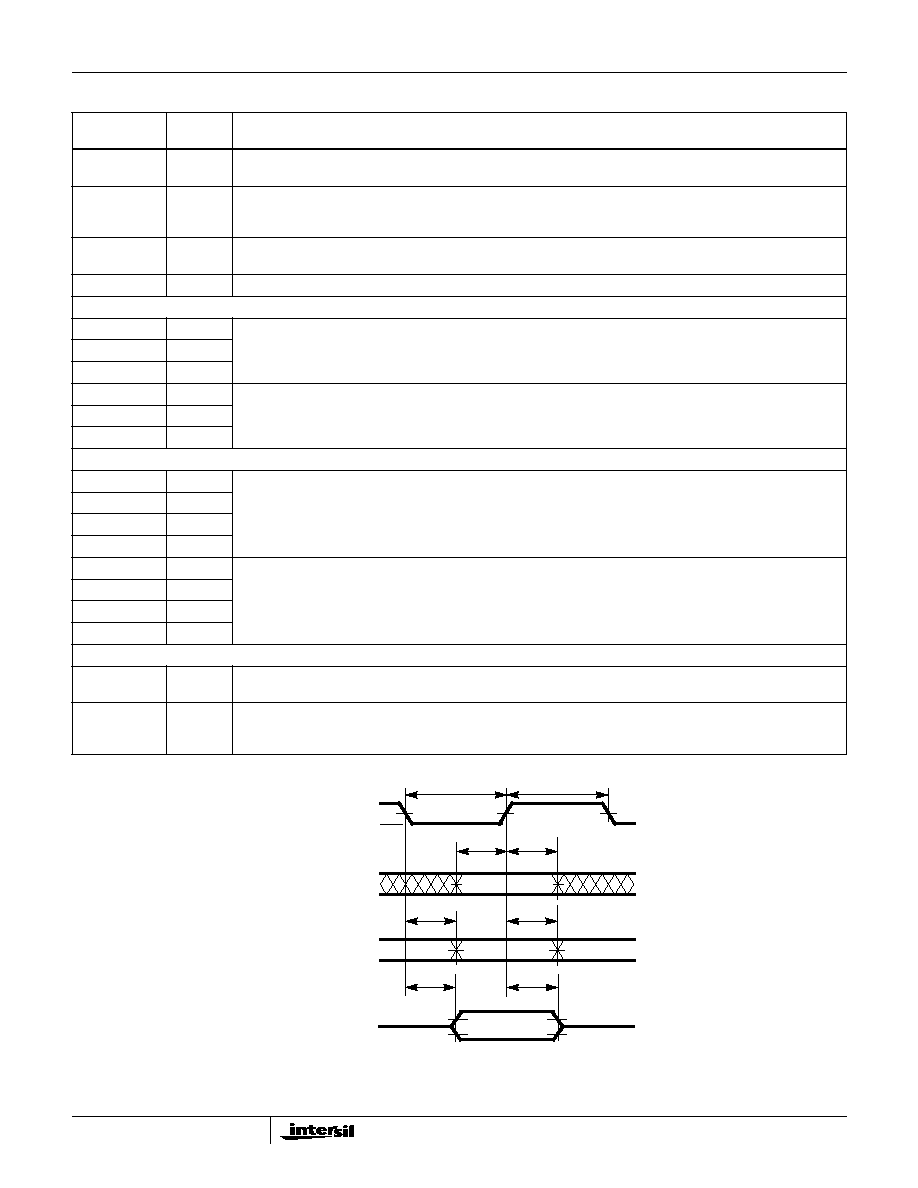
FIGURE 1. AC DRIVE AND MEASURE POINTS - CLK INPUT
4.0V
0.5V
4.0V
0.5V
t
PULSE WIDTH
t
HOLD
t
SETUP
2.25V
t
VALID
t
HOLD
t
DELAY
2.25V
TYPICAL
CLOCK OR
STROBE
TYPICAL
INPUT
TYPICAL
OUTPUT
TYPICAL
DATA
OUTPUT
2.25V
2.25V
2.75V
1.75V
2.75V
1.75V
2.25V
2.25V
2.25V
t
DELAY
t
PULSE WIDTH
HS-RTX2010RH

6
Timing Diagrams
NOTES:
1. NORMAL CYCLE: This waveform describes a normal PCLK cycle and a PCLK cycle with a Wait state.
2. EXTENDED CYCLE: This waveform describes a PCLK cycle for a USER memory access or an external ASIC Bus read cycle when the CYCEXT
bit or ARCE bit is set.
3. EXTENDED CYCLE: This waveform describes a GIO cycle for an external ASIC Bus read when the ARCE bit is set.
4. An active HIGH signal on the RESET input is guaranteed to reset the processor if its duration is greater than or equal to 4 rising edges of ICLK
plus 1/2 ICLK cycle setup and hold times. If the RESET input is active for less than four rising edges of ICLK, the processor will not reset.
FIGURE 2. CLOCK AND WAIT TIMING
FIGURE 3. TIMER/COUNTER TIMING
t
3
ICLK
TCLK
WAIT
PCLK
(NOTE 2)
PCLK
(NOTE 1)
GIO
(NOTE 3)
t
2
t
1
t
19
t
13
t
12
t
5
t
4
t
11
t
5
t
20
t
15
t
20
t
17
t
16
t
51
t
50
t
4
t
7
t
8
t
6
EI5 - EI3
HS-RTX2010RH

7
NOTES:
5. If both LDS and UDS are low, no memory access is taking place in the current cycle. This only occurs during streamed instructions that do not
access memory.
6. During a streamed single cycle instruction, the Memory Data Bus is driven by the processor.
FIGURE 4. MEMORY BUS TIMING
NOTES:
7. GIO remains high for internal ASIC bus cycles.
8. GR/W goes low and GD is driven for all ASIC write cycles, including internal ones.
9. During non-ASIC write cycles, GD is not driven by the HS-RTX2010RH. Therefore, it is recommended that all GD pins be pulled to VCC or GND
to minimize power supply current and noise.
10. t
40B
and t
41B
specifications are for Streamed Mode of operation only.
FIGURE 5. ASIC BUS TIMING
Timing Diagrams
(Continued)
t
26
t
28
t
31
t
35
t
29
t
32
t
34
t
33
PCLK
MA
MD
IN
MD
OUT
LDS
UDS
NEW
BOOT
MR/W
t
21
t
22
t
48
t
50
t
51
t
49
t
52
t
56
t
54
t
58
t
42
t
43
t
40A, B
t
41A, B
t
62
t
61
t
63
t
65
GA
PCLK
ICLK
GIO
GR/W
GD
IN
GD
OUT
t
69
HS-RTX2010RH

8
NOTES:
11. Events in an interrupt sequence are as follows:
e
1
. The Interrupt Controller samples the interrupt request inputs on the rising edge of PCLK. If NMI rises between e
1
and the rising edge of
PCLK prior to e
5
, the interrupt vector will be for NMI.
e
2
. If any interrupt requests were sampled, the Interrupt Controller issues an interrupt request to the core on the falling edge of PCLK.
e
3
. The core samples the state of the interrupt requests from the Interrupt Controller on the falling edge of PCLK. If INTSUP is high, maskable
interrupts will not be detected at this time.
e
4
. When the core samples an interrupt request on the falling edge of PCLK, an Interrupt Acknowledge cycle will begin on the next rising edge
of PCLK.
e
5
. Following the detection of an interrupt request by the core, an Interrupt Acknowledge cycle begins. The interrupt vector will be based on the
highest priority interrupt request active at this time.
12. t
44
is only required to determine when the Interrupt Acknowledge cycle will occur.
13. Interrupt requests should be held active until the Interrupt Acknowledge cycle for that interrupt occurs.
FIGURE 6. INTERRUPT TIMING: WITH INTERRUPT SUPPRESSION
FIGURE 7. INTERRUPT TIMING: WITH NO INTERRUPT SUPPRESSION
Timing Diagrams
(Continued)
MA
INTA
INTSUP
PCLK
e
1
e
2
e
3
e
4
e
5
t
44
t
46
t
47
t
46
t
47
t
67
t
68
t
28
t
26
EI
INT VECTOR
e
1
e
2
e
4
e
5
t
44
t
46
t
47
t
67
t
68
t
26
t
28
MA
INTA
INTSUP
PCLK
E I
INT VECTOR
HS-RTX2010RH

9
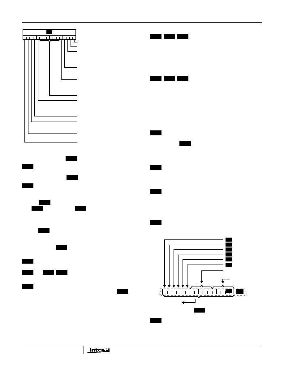
HS-RTX2010RH Microcontroller
The HS-RTX2010RH is designed around the RTX Processor
core, which is part of the Intersil Standard Cell Library.
This processor core has eight 16-bit internal registers, an
ALU, internal data buses, and control hardware to perform
instruction decoding and sequencing.
On-chip peripherals which the HS-RTX2010RH includes are
Memory Page Controller, an Interrupt Controller, three
Timer/Counters, and two Stack Controllers. Also included
are a Multiplier-Accumulator (MAC), a Barrel Shifter, and a
Leading Zero Detector for floating point support.
Off-chip user interfaces provide address and data access to
Main Memory and ASIC I/O devices, user defined interrupt
signals, and Clock/Reset controls.
Figure 9 shows the data paths between the core, on-chip
peripherals, and off-chip interfaces.
The HS-RTX2010RH microcontroller is based on a two-stack
architecture. These two stacks, which are Last-In-First-Out
(LIFO) memories, are called the Parameter Stack and the
Return Stack.
Two internal registers,
and
, provide the top
two elements of the 16-bit wide Parameter Stack, while the
remaining elements are contained in on-chip memory ("stack
memory").
The top element of the Return Stack is 21 bits wide, and is
stored in registers
and
, while the remaining
elements are contained in stack memory.
The highly parallel architecture of the RTX is optimized for
minimal Subroutine Call/Return overhead. As a result, a
Subroutine Call takes one Cycle, while a Subroutine Return
is usually incorporated into the preceding instruction and
does not add any processor cycles. This parallelism
provides for peak execution rates during simultaneous bus
operations which can reach the equivalent of 32 million
Forth language operations per second at a clock rate of
8MHz. Typical execution rates exceed 8 million operations
per second.
Intersil factory applications support for this device is limited.
RTS-C C-Compiler support is provided by Highland Software
at highlandsoft@compuserve.com. Development system
tools are supported by Micro Processor Engineering Limited
(UK) at 441 703 631441. A HS-RTX2010RH programmers
reference manual can be obtained through your local Intersil
Sales Office.
NOTES:
14. Events in an interrupt sequence are as follows:
e
1
. The Interrupt Controller samples the interrupt request inputs on the rising edge of PCLK. If NMI rises between e
1
and the rising edge of
PCLK prior to e
5
, the interrupt vector will be for NMI.
e
2
. If any interrupt requests were sampled, the Interrupt Controller issues an interrupt request to the core on the falling edge of PCLK.
e
4
. When the core samples an interrupt request on the falling edge of PCLK, an Interrupt Acknowledge cycle will begin on the next rising edge
of PCLK.
e
5
. Following the detection of an interrupt request by the core, an Interrupt Acknowledge cycle begins. The interrupt vector will be based on the
highest priority interrupt request active at this time.
15. t
44
is only required to determine when the Interrupt Acknowledge cycle will occur.
16. Interrupt requests should be held active until the Interrupt Acknowledge cycle for that interrupt occurs.
17. NMI has a glitch filter which requires the signal that initiates NMI last at least two rising and two falling edges of ICLK.
FIGURE 8. NON-MASKABLE INTERRUPT TIMING
Timing Diagrams
(Continued)
t
44
e
1
e
2
e
4
e
5
PCLK
NMI
MA
INTA
NMI
VECTOR
t
67
t
68
t
26
t
28
TOP
NEXT
I
IPR
HS-RTX2010RH

10
HS-RTX2010RH Operation
Control of all data paths and the Program Counter Register,
(
), is provided by the Instruction Decoder. This hardware
determines what function is to be performed by looking at
the contents of the Instruction Register, (
), and
subsequently determines the sequence of operations
through data path control.
Instructions which do not perform memory accesses execute
in a single clock cycle while the next instruction is being
fetched.
As shown in Figure 10, the instruction is latched into
at
the beginning of a clock cycle. The instruction is then decoded
by the processor. All necessary internal operations are
performed simultaneously with fetching the next instruction.
Instructions which access memory require two clock cycles
to be executed. During the first cycle of a memory access
instruction, the instruction is decoded, the address of the
memory location to be accessed is placed on the Memory
Address Bus (MA19-MA01), and the memory data
(MD15-MD00), is read or written. During the second cycle,
ALU operations are performed, the address of the next
instruction to be executed is placed on the Memory Address
Bus, and the next instruction is fetched, as indicated in the
bottom half of Figure 10.
BYTE
SWAP
HS-RTX2010RH
OFF-CHIP
USER
INTERFACES
TIMER/COUNTERS
TP0
TP1
TP2
TC0
TC1
TC2
ALU
Y
T
PC
I
TOP
CR
MD
SR
CONTROL
STACK
IMR
IVR
IBC
CONTROL
INTERRUPT
(NO
TE)
CONTROL
PAGE
MEMORY
CLOCK AND
CONTROL
RESET
INTERFACE
MEMORY BUS
INTERFACE
ASIC BUS
DPR
IPR
UPR
CPR
UBR
SPR
SUR
SVR
EI5-EI3
EI2-EI1
INT
A
NMI
INTSUP
ICLK
W
AIT
PCLK
TCLK
RESET
UDS
LDS
NEW
BOO
T
MR/W
MA19-
MA01
MD15-
MD00
GR/W
GIO
GA2-
GA0
GD15-
GD00
-
1
+1
INSTRUCTION
DECODER
IR
LEADING ZERO
DETECTOR
BARREL
SHIFTER
16 x 16
MAC
MXR
MHR
MLR
256 x 21
RETURN
MEMORY
STACK
256 x 16
PARAMETER
MEMORY
STACK
NEXT
NOTE:
contains the 5 most significant bits (20-16) of the top element of the Return Stack.
FIGURE 9. HS-RTX2010RH FUNCTIONAL BLOCK DIAGRAM
IPR
PC
IR
IR
HS-RTX2010RH
11
RTX Data Buses and Address Buses
The RTX core bus architecture provides for unidirectional
data paths and simultaneous operation of some data buses.
This parallelism allows for maximum efficiency of data flow
internal to the core.
Addresses for accessing external (off-chip) memory or
ASIC devices are output via either the Memory Data Bus
(MA19-MA01) or the ASIC Address Bus (GA02-GA00). See
Table 3. External data is transferred by the ASIC Data Bus
(GD15-GD00) and the Memory Data Bus (MD15-MD00),
both of which are bidirectional.
RTX Internal Registers
The core of the HS-RTX2010RH is a macrocell available
through the Intersil Standard Cell Library. This core contains
eight 16-bit internal registers, which may be accessed
implicitly or explicitly, depending upon the register accessed
and the function being performed.
: The Top Register contains the top element of the
Parameter Stack++.
is the implicit data source or
destination for certain instructions, and has no ASIC address
assignment. The contents of this register may be directed to
any I/O device or to any processor register except the
Instruction Register.
is also the T input to the ALU.
Input to
must come through the ALU. This register
also holds the most significant 16 bits of 32-bit products and
32-bit dividends.
: The Next Register holds the second element of the
Parameter Stack.
is the implicit data source or
destination for certain instructions, and has no ASIC address
assignment. During a stack "push", the contents of
are transferred to stack memory, and the contents of
are put into
. This register is used to hold the least
significant 16 bits of 32-bit products. Memory data is
accessed through
, as described in the Memory
Access section of this document.
: The Instruction Register is actually a latch which
contains the instruction currently being executed, and has no
ASIC address assignment. In certain instructions, an
operand can be embedded in the instruction code, making
the implicit source for that operand (as in the case of
short literals). Input to this register comes from Main
Memory (see Tables 6 thru 22 for code information).
: The Configuration Register is used to indicate and
control the current status/setup of the RTX microcontroller,
through the bit assignments shown in Figure 11. This
register is accessed explicitly through read and write
operations, which cause interrupts to be suppressed for one
cycle, guaranteeing that the next instruction will be
performed before an Interrupt Acknowledge cycle is allowed
to be performed.
CYCLE
CLOCK
SECOND
BEGIN
CONCURRENT
OPERATIONS
EXECUTION SEQUENCE WITH NO MEMORY DATA ACCESS:
EXECUTION SEQUENCE WITH MEMORY DATA ACCESS:
CYCLE
CLOCK
FIRST
END OF
FETCH
DECODE
DECODE
OPERATIONS
CONCURRENT
PCLK
MEMORY DATA
READ OR WRITE
PERFORM INTERNAL OPERATIONS AND
ALU OPERATIONS, AS REQUIRED
CYCLE
CLOCK
FIRST
END OF
CYCLE
CLOCK
SECOND
BEGIN
CYCLE
CLOCK
FIRST
BEGIN
ASIC BUS OPERATIONS
SECOND
CLOCK
CYCLE
END OF
CYCLE
CLOCK
FIRST
BEGIN
ADDRESS OF
MEMORY
LOCATION
IS PLACED ONTO
MA19-MA01
BUS
PLACE ADDRESS OF
NEXT INSTRUCTION
ONTO MA19-MA01
FETCH NEXT
INSTRUCTION
PERFORM ALU OPERATIONS
INSTRUCTION
LATCHES INTO
ADDRESS OF
NEXT
INSTRUCTION
IS PLACED ONTO
MA19-MA01
BUS
INSTRUCTION
LATCHES
IR
INTO
IR
FIGURE 10. INSTRUCTION EXECUTION SEQUENCE
TOP
TOP
TOP
TOP
NEXT
EXT
NEXT
TOP
NEXT
NEXT
IR
IR
CR
HS-RTX2010RH
12
: The Program Counter Register contains the address
of the next instruction to be fetched from Main Memory. At
RESET, the contents of
are set to 0.
: The Index Register contains 16 bits of the 21-bit top
element of the Return Stack, and is also used to hold the
count for streamed and loop instructions (see Figure 19). In
addition,
can be used to hold data and can be written
from
. The contents of
may be accessed in
either the push/pop mode in which values are moved to/from
stack memory as required, or in the read/write mode in
which the stack memory is not affected. The ASIC address
used for
determines what type of operation will be
performed (see Table 5). When the Streamed Instruction
Mode (see RTX Programmer's Reference Manual) is used, a
count is written to
and the next instruction is executed
that number of times plus one (i.e., count + 1).
: The Multi-Step Divide Register holds the divisor
during Step Divide operations, while the 32-bit dividend is in
and
.
may also be used as a general
purpose scratch pad register.
: The Square Root Register holds the intermediate
values used during Step Square Root calculations.
may also be used as a general purpose scratch pad register.
On-Chip Peripheral Registers
The HS-RTX2010RH has an on-chip Interrupt Controller, a
Memory Page Controller, two Stack Controllers, three
Timer/Counters, a Multiplier-Accumulator, a Barrel Shifter,
and a Leading Zero Detector. Each of these peripherals
utilizes on-chip registers to perform its functions.
Timer/Counter Registers
,
,
: The Timer/Counter Registers are
16-bit read-only registers which contain the current count
value for each of the three Timer/Counters. The counter is
decremented at each rising clock edge of TCLK. Reading
from these registers at any time does not disturb their
contents. The sequence of Timer/Counter operations is
shown in Figure 23 in the Timer/Counters section.
,
,
: The Timer Preload Registers are
write-only registers which contain the initial 16-bit count
values which are written to each timer. After a timer counts
down to zero, the preload register for that timer reloads its
initial count value to that timer register at the next rising clock
edge, synchronously with TCLK. Writing to these registers
causes the count to be loaded into the corresponding Timer/
Counter register on the following cycle.
Multiplier-Accumulator (MAC) Registers:
: The Multiplier High Product Register holds the most
significant 16 bits of the 32-bit product generated by the RTX
Multiplier. If the
register's ROUND bit is set, this
register contains the rounded 16-bit output of the multiplier.
In the Accumulator context, this register holds the middle 16
bits of the MAC.
: The Multiplier Lower Product Register holds the least
significant 16 bits of the 32-bit product generated by the RTX
Multiplier. It is also the register which holds the least
significant 16 bits of the MAC Accumulator.
: The MAC Extension Register holds the most significant
16 bits of the MAC Accumulator. When using the Barrel Shifter,
this register holds the shift count. When using the Leading Zero
Detector, the leading zero count is stored in this register.
Interrupt Controller Registers
: The Interrupt Vector Register is a read-only register
which holds the current Interrupt Vector value. See Figure 12
and Table 4.
: The Interrupt Base/Control Register is used to store
the Interrupt Vector base address and to specify
configuration information for the processor, as indicated by
the bit assignments in Figure 13.
R/W; CARRY
R/W; COMPLEX CARRY
SET INTERRUPT DISABLE;
0 = INT. ENABLED;
1 = INT. DISABLED
WRITE - ONLY (READS AS 0);
R/W; BYTE ORDER BIT
0 = ADDRESSING MODE 0
1 = ADDRESSING MODE 1
RESETS TO 0. MODES:
RESERVED (NOTE)
R/W; BOOT
DRIVES OUTPUT SIGNAL
TO SELECT BOOT ROM;
INTERRUPT LATCH
READ ONLY;
DISABLE STATUS
READ ONLY; INTERRUPT
ARCE; ASIC READ CYCLE EXTEND
WHEN SET EXTENDS CYCLE ON
NMI MODE
1 = RETURN FROM NMI POSSIBLE
0 = NO RETURN FROM NMI
RESERVED (NOTE)
EXTERNAL ASIC READS
(RTX 2000 MODE)
CR
5
6
7
8
0
1
2
3
4
9
1 1
1
1
1
1
5 4 3 2 1 0
NOTE: Always read as ``0''. Should be set = 0 during Write operations.
FIGURE 11.
BIT ASSIGNMENTS
CR
PC
PC
I
I
TOP
I
I
I
MD
TOP
EXT
MD
SR
SR
TC0
TC1
TC2
TP0
TP1
TP2
MHR
IBC
MLR
MXR
IVR
ALL ZEROS
VECTOR ADDRESS
(SEE TABLE 1)
0
1
2
3
4
5
6
7
11
8
9
10
12
13
14
15
IVR
BIT 10
BIT 11
BIT 12
BIT 15
BIT 14
BIT 13
IBC
IBC
IBC
IBC
IBC
IBC
MA15-MA00
IBC
FIGURE 12.
BIT ASSIGNMENTS
IVR
IBC
HS-RTX2010RH

13
: The Interrupt Mask Register has a bit assigned for
each maskable interrupt which can occur. When a bit is set,
the interrupt corresponding to that bit will be masked. Only
the Non-Maskable Interrupt (NMI) cannot be masked. See
Figure 14 for bit assignments for this register.
Stack Controller Registers
: The Stack Pointer Register holds the stack pointer
value for each stack. Bits 0-7 represent the next available
stack memory location for the Parameter Stack, while bits 8-
15 represent the next available stack memory location for the
Return Stack. These stack pointer values must be accessed
together, as
. See Figure 15.
: The Stack Overflow Limit Register is a write-only
register which holds the overflow limit values (0 to 255) for
the Parameter Stack (bits 0-7) and the Return Stack (bits
8-15). These values must be written together. See Figure 16.
: The Stack Underflow Limit Register holds the
underflow limit values for the Parameter Stack and the
Return Stack. In addition, this register is utilized to define the
use of substacks for both stacks. These values must be
accessed together. See Figure 17.
0
1
2
3
4
5
6
7
8
9
1514
12
13
10
READ-ONLY; FATAL
STACK ERROR FLAG
READ-ONLY; PARAMETER
STACK UNDERFLOW FLAG
READ-ONLY; PARAMETER
STACK OVERFLOW FLAG
READ-ONLY; RETURN
STACK UNDERFLOW FLAG
READ-ONLY; RETURN
STACK OVERFLOW FLAG
SVR
IBC
PARAMETER STACK
RETURN STACK FATAL ERROR
DPRSEL: SELECTS
= 1: SELECT
= 0: SELECT
PAGE REGISTER FOR
DATA MEMORY ACCESS
SUR
CPR
DPR
ROUND: MULTIPLIER
CONTROL BIT; SELECTS
ROUNDING OF 16 x 16
BIT MULTIPLICATION
= 1: ROUNDED 16-BIT
PRODUCT
= 0: UNROUNDED
32-BIT PRODUCT
INPUT SIGNALS: TCLK
OR EI5 - EI3 (TABLE 6)
SELECT TIMER/COUNTER
CYCEXT: ALLOWS
EXTENDED CYCLE LENGTH
FOR USER MEMORY
INSTRUCTION CYCLES; SEE
CLOCK AND WAIT
TIMING DIAGRAMS
MA14
MA15
MA12
MA13
MA10
MA11
INTERR
UPT VECT
OR
INTERR
UPT SECTION)
B
ASE (SEE THE
11
FATAL ERROR
FIGURE 13.
BIT ASSIGNMENTS
IBC
IMR
RSV, RETURN STACK
OVERFLOW
PSV, PARAMETER STACK
OVERFLOW
RSU, RETURN STACK
UNDERFLOW
PSU, PARAMETER STACK
UNDERFLOW
EI1
(EXTERNAL INPUT PIN)
EI2
TCI 0
TCI 1
TCI 2
EI3
EI4
EI5
SWI
IMR
15 14
12
13
8
9
10
11
0
1
2
3
4
5
6
7
RESERVED (NOTE)
RESERVED (NOTE)
NOTE: Always read as ``0''. Should be set = 0 during Write operations.
FIGURE 14.
BIT ASSIGNMENTS
IMR
SPR
SPR
SVR
SUR
8
9
PSP, PARAMETER STACK
POINTER
RSP, RETURN STACK
POINTER
0
1
2
3
4
5
6
7
SPR
10
11
15 14 1312
FIGURE 15.
BIT ASSIGNMENTS
SPR
PVL: PARAMETER
STACK OVERFLOW LIMIT.
RVL: RETURN STACK
OVERFLOW LIMIT.
SVR
0
1
2
3
4
5
6
7
8
9
14
15
13 12 11 10
NUMBER OF WORDS FROM
TOP OF CURRENT SUBSTACK
NUMBER OF WORDS FROM
TOP OF CURRENT SUBSTACK
FIGURE 16.
BIT ASSIGNMENTS
SVR
HS-RTX2010RH

14
Memory Page Controller Registers
: The Code Page Register contains the value for the
current 32K-word Code page. See Figure 18 for bit field
assignments.
: The Index Page Register extends the Index Register
(
) by 5 bits; i.e., when a Subroutine Return is performed,
the
contains the Code page from which the subroutine
was called, and comprises the 5 most significant bits of the
top element of the Return Stack. See Figure 19. During
nonsubroutine operation, writing to
causes the current
Code page value to be written to
. Reading or writing
directly to
does not push the Return Stack.
: The Data Page Register contains the value for the
current 32K-word Data page. See Figure 20 for bit field
assignments.
: The User Page Register contains the value for the
current User page. See Figure 21 for bit field assignments.
: The User Base Address Register contains the base
address for User Memory Instructions. See Figure 21 for bit
field assignments.
0
1
2
3
4
5
6
7
8
9
PSF: PARAMETER STACK
START FLAG
PSU: PARAMETER
0 - 31 WORDS FROM
BOTTOM OF SUBSTACK
STACK UNDERFLOW LIMIT
RSF: RETURN STACK
START FLAG
RSU: RETURN STACK
0 - 31 WORDS FROM
BOTTOM OF SUBSTACK
UNDERFLOW LIMIT
RETURN SUBSTACK BITS:
= 00: EIGHT 32 WORD STACKS
= 01: FOUR 64 WORD STACKS
SUR
15 14 13 12 1110
PARAMETER SUBSTACK BITS:
= 00: EIGHT 32 WORD STACKS
= 01: FOUR 64 WORD STACKS
= 10: TWO 128 WORD STACKS
= 11: ONE 256 WORD STACK
= 10: TWO 128 WORD STACKS
= 11: ONE 256 WORD STACK
FIGURE 17.
BIT ASSIGNMENTS
SUR
CPR
0
1
2
3
4
5
6
7
11
8
9
10
12
13
14
15
CPR
MA16
MA17
MA18
MA19
RESERVED
(NOTE)
NOTE: Always read as ``0''. Should be set = 0 during Write operations.
FIGURE 18.
BIT ASSIGNMENTS
CPR
IPR
I
IPR
I
IPR
IPR
DPR
UPR
UBR
BIT ASSIGNMENTS DURING NON-SUBROUTINE OPERATIONS
I
IPR
9
0
1
2
3
4
5
6
7
8
BIT ASSIGNMENTS DURING SUBROUTINE OPERATIONS
DEFINES RETURN ADDRESS
TYPE OF RETURN
= 1: INTERRUPT RETURNS:
= 0: SUBROUTINE RETURNS:
STORED DURING INTERRUPT
WHERE DPRSEL BIT IS
OR SUBROUTINE CALL
I
IPR
9
0
1
2
3
4
5
6
7
8
USED FOR TEMPORARY
STORAGE OF VARIABLES,
LOOP COUNTS, AND
STREAM COUNTS
CURRENT CODE
PAGE VALUE
0
2
9
1
8
1
7
1
6
1
5
1
4
1
3
1
2
1
1
1
0
1
0
2
9
1
8
1
7
1
6
1
5
1
4
1
3
1
2
1
1
1
0
1
FIGURE 19.
AND
BIT ASSIGNMENTS
I
IPR
0
1
2
3
4
5
6
7
11
8
9
10
12
13
14
15
DPR
MA16
MA17
MA18
MA19
RESERVED
(NOTE)
NOTE: Always read as ``0''. Should be set = 0 during Write operations.
FIGURE 20.
BIT ASSIGNMENTS
DPR
0
1
2
3
4
5
6
7
11
8
9
10
12
13
14
15
USER PAGE
REGISTER
UBR
MA15 - MA06
0
1
2
3
4
5
6
7
11
8
9
10
12
13
14
15
I R
0
1
2
3
4
5
6
7
11
8
9
10
12
13
14
15
UPR
MA19
MA18
MA17
MA16
NOT USED TO GENERATE
THIS ADDRESS
INSTRUCTION
REGISTER
RESER
VED
USER BASE
REGISTER
ADDRESS
RESERVED
MA05
MA04
MA03
MA02
MA01
(NOTE)
(NO
TE)
NOTE: Always read as ``0''. Should be set = 0 during Write operations.
FIGURE 21.
AND
BIT ASSIGNMENTS
UPR
UBR
HS-RTX2010RH
15
Initialization of Registers
Initialization of the on-chip registers occurs when a HIGH
level on the RTX RESET pin is held for a period of greater
than or equal to four rising edges of ICLK plus 1/2 ICLK
cycle setup and hold times. While the RESET input is HIGH,
the TCLK and PCLK clock outputs are held reset in the LOW
state.
Table 1 shows initialization values and ASIC addresses for
the on-chip registers. As indicated, both the
and the
are cleared and execution begins at page 0, word 0
when the processor is reset.
The RESET has a Schmitt trigger input, which allows the
use of a simple RC network for generation of a power-on
RESET signal. This helps to minimize the circuit board
space required for the RESET circuit.
To ensure reliable operation even in noisy embedded control
environments, the RESET input is filtered to prevent a reset
caused by a glitch of less than four ICLK cycles duration.
PC
CPR
TABLE 1. REGISTER INITIALIZATION AND ASIC ADDRESS ASSIGNMENTS
REGISTER
HEX
ADDR
INITIALIZED
CONTENTS
DESCRIPTION/COMMENTS
0000 0000 0000 0000
Top Register
1111 1111 1111 1111
Next Register
0000 0000 0000 0000
Instruction Register
00H 01H
02H
1111 1111 1111 1111
Index Register
03H
0100 0000 0000 1000
Configuration Register: Boot = 1; Interrupts Disabled; Byte Order = 0.
04H
1111 1111 1111 1111
Multi-Step Divide Register
06H
0000 0010 0000 0000
Square Root Register
07H
0000 0000 0000 0000
Program Counter Register
08H
0000 0000 0000 0000
Interrupt Mask Register
09H
0000 0000 0000 0000
Stack Pointer Register: The beginning address for each stack is set to a value of `0'.
0AH
0000 0111 0000 0111
Stack Underflow Limit Register
0BH
0000 0010 0000 0000
Interrupt Vector Register: Read only; this register holds the current Interrupt Vector
value, and is initialized to the "No Interrupt" value.
0BH
1111 1111 1111 1111
Stack Overflow Limit Register: Write-only; Each stack limit is set to its maximum value.
0CH
0000 0000 0000 0000
Index Page Register
0DH
0000 0000 0000 0000
Data Page Register: The Data Address Page is set for page `0'.
0EH
0000 0000 0000 0000
User Page Register: The User Address Page is set for page `0'.
0FH
0000 0000 0000 0000
Code Page Register: The Code Address Page is set for page `0'.
10H
0000 0000 0000 0000
Interrupt Base/Control Register
11H
0000 0000 0000 0000
User Base Address Register: The User base address is set to `0' within the User page.
12H
0000 0000 0000 0000
MAC Extension Register
/
13H
0000 0000 0000 0000
Timer/Counter Register 0: Set to time out after 65536 clock periods or events.
/
14H
0000 0000 0000 0000
Timer/Counter Register 1: Set to time out after 65536 clock periods or events.
/
15H
0000 0000 0000 0000
Timer/Counter Register 2: Set to time out after 65536 clock periods or events.
16H
0000 0000 0000 0000
Multiplier Lower Product Register
17H
0000 0000 0000 0000
Multiplier High Product Register
TOP
NEXT
IR
I
CR
MD
SR
PC
IMR
SPR
SUR
IVR
SVR
IPR
DPR
UPR
CPR
IBC
UBR
MXR
TC0
TP0
TC1
TP1
TC2
TP2
MLR
MHR
HS-RTX2010RH
16
Dual Stack Architecture
The HS-RTX2010RH features a dual stack architecture. The
two 256-word stacks are the Parameter Stack and the
Return Stack, both of which may be accessed in parallel by a
single instruction, and which minimize overhead in passing
parameters between subroutines. The functional structure of
each of these stacks is shown in Figure 22.
The Parameter Stack is used for temporary storage of data
and for passing parameters between subroutines. The top two
elements of this stack are contained in the
and
registers of the processor, and the remainder of this stack is
located in stack memory. The stack memory assigned to the
Parameter Stack is 256 words deep by 16 bits wide.
The Return Stack is used for storing return addresses when
performing Subroutine Calls, or for storing values temporarily.
Because the HS-RTX2010RH uses a separate Return Stack, it
can call and return from subroutines and interrupts with a
minimum of overhead. The Return Stack is 21 bits wide. The
16-bit Index Register,
, and the 5-bit Index Page Register,
, hold the top element of this stack, while the remaining
elements are located in stack memory. The stack memory
portion of the Return Stack is 21 bits wide, by 256 words deep.
The data on the Return Stack takes on different meaning,
depending upon whether the Return Stack is being used for
temporary storage of data or to hold a return address during
a subroutine operation (Figure 19).
HS-RTX2010RH Stack Controllers
The two stacks of the HS-RTX2010RH are controlled by
identical Programmable Stack Controllers.
The operation of the Programmable Stack Controllers
depends on the contents of three registers. These registers
are
, the Stack Pointer Register,
, the Stack
Overflow Limit Register, and
, the Stack Underflow
Limit Register (see Figures 15, 16, and 17).
contains the address of the next stack memory
location to be accessed in a stack push (write) operation.
After a push, the
is incremented (post-increment
operation). In a stack pop (read) operation, the stack
memory location with an address one less than the
will be accessed, and then the
will be decremented
(pre-decrement operation). At start-up, the first stack
location to have data pushed into it is location zero.
Upper and lower limit values for the stacks are set into the
Stack Overflow Limit Register and in the Stack Underflow
Limit Register. These values allow interrupts to be generated
prior to the occurrence of stack overflow or underflow error
conditions (see section on Stack Error Conditions for more
detail). Since the HS-RTX2010RH can take up to four clock
cycles to respond to an interrupt, the values set in these
registers should include a safety margin which allows valid
stack operation until the processor executes the interrupt
service routine.
TOP
NEXT
I
IPR
SPR
SVR
SUR
SPR
SPR
SPR
SPR
(ON-CHIP)
STACK MEMORY
PARAMETER STACK
8
9
10
11
12
0
7
5
6
1
2
3
4
13
14
15
8
9
10
11
12
0
7
5
6
1
2
3
4
13
14
15
RETURN STACK
(ON-CHIP)
STACK MEMORY
RVL
PVL
RSU
RSP
1
2
8
9
0
1 0
2
3
4
5
6
7
3
4
5
6
7
8
9
1
1
1
1
1
1
1
1
1
0
1
2
I
IPR
PSU
PSP
TOP
NEXT
8
9
10
11
12
13
14
15
0
7
5
6
1
2
3
4
SVR
8
9
10
11
12
13
14
15
0
7
5
6
1
2
3
4
SPR
8
9
10
11
12
13
14
15
0
7
5
6
1
2
3
4
SUR
FIGURE 22. DUAL STACK ARCHITECTURE
HS-RTX2010RH

17
Substacks
Each 256-word stack may be subdivided into up to eight 32
word substacks, four 64 word substacks, or two 128 word
substacks. This is accomplished under hardware control for
simplified management of multiple tasks. Stack size is
selected by writing to bits 1 and 2 of the
for the
Parameter Stack, and bits 9 and 10 for the Return Stack.
Substacks are implemented by making bits 5-7 of the
(for the Parameter Stack) and bits 13-15 of the
(for the
Return Stack) control bits. For example, if there were eight
32 word substacks implemented in the Parameter Stack, bits
5-7 of the
are not incremented, but instead are used
as an offset pointer into the Parameter Stack to indicate the
beginning point (i.e., sub stack number) of each 32 word
substack implemented. Because of this, a particular
substack is selected by writing a value which contains both
the stack pointer value and the substack number to the
.
Each stack has a Stack Start Flag (PSF and RSF) which
may be used for implementing virtual stacks. For the
Parameter Stack, the Start Flag is bit zero of the
, and
for the Return Stack it is bit eight. If the Stack Start Flag is
one, the stack starts at the bottom of the stack or substack
(location 0). If the Stack Start Flag is zero, the substack
starts in the middle of the stack. An exception to this occurs
if the overflow limit in
is set for a location below the
middle of the stack. In this case, the stacks always start at
the bottom locations. See Table 2 for the possible stack
configurations. Manipulating the Stack Start Flag provides a
mechanism for creating a virtual stack in memory which is
maintained by interrupt driven handlers.
Possible applications for substacks include use as a
recirculating buffer (to allow quick access for a series of
repeated values such as coefficients for polynomial
evaluation or a digital filter), or to log a continuous stream of
data until a triggering event (for analysis of data before and
after the trigger without having to store all of the incoming
data). The latter application could be used in a digital
oscilloscope or logic analyzer.
Stack Error Conditions
Stack errors include overflow, underflow, and fatal errors.
Overflows occur when an attempt is made to push data onto
a full stack. Since the stacks wrap around, the result is that
existing data on the stack will be overwritten by the new data
when an overflow occurs. Underflows occur when an attempt
is made to pop data off an empty stack, causing invalid data
to be read from the stack. In both cases, a buffer zone may
be set up by initializing
and
so that stack error
interrupts are generated prior to an actual overflow or
underflow. The limits may be determined from the contents
of
and
using Table 2. The state of all stack
errors may be determined by examining the five least
significant bits of
, where the stack error flags may be
read but not written to. All stack error flags are cleared
whenever a new value is written to
.
Fatal Stack Error: Each stack can also experience a fatal
stack error. This error condition occurs when an attempt is
made to push data onto or to pop data off of the highest
location of the substack. It does not generate an interrupt
(since the normal stack limits can be used to generate the
interrupt). The fatal errors for the stacks are logically OR'ed
together to produce bit 0 of the Interrupt Base Control
Register, and they are cleared whenever
is written to.
The implication of a fatal error is that data on the stack may
have been corrupted or that invalid data may have been read
from the stack.
HS-RTX2010RH Timer/Counters
The HS-RTX2010RH has three 16-bit timers, each of which
can be configured to perform timing or event counting. All
decrement synchronously with the rising edge of TCLK.
Timer registers are readable in a single machine cycle.
The timer selection bits of the
determine whether a
timer is to be configured for external event counting or
internal time-base timing. This configures the respective
counter clock inputs to the on-chip TCLK signal for internal
timing, or to the EI5 - EI3 input pins for external signal event
counting. EI5, EI4, and EI3 are synchronized internally with
TCLK. See Table 3 for Timer/Clock selection by
bit
values.
The timers (
,
and
) are all free-running,
and when they time out, they reload automatically with the
programmed initial value from their respective Timer Pre
load Registers (
,
, and
), then continue timing or counting.
Each timer provides an output to the Interrupt Controller to
indicate when a time-out for the timer has occurred.
The HS-RTX2010RH can determine the state of a timer at
any time either by reading the timer's value, or upon a time-
out by using the timer's interrupt (see the Interrupt Controller
section for more information about how timer interrupts are
handled). Figure 23 shows the sequence of Timer/Counter
operations.
SUR
SPR
SPR
SPR
SPR
SUR
SVR
SVR
SUR
SVR
SUR
IBC
SPR
SPR
IBC
IBC
TC0
TC1
TC2
TPO
TC0
TP1
TC1
TP2
TC2
HS-RTX2010RH

18
TABLE 2. STACK/SUBSTACK CONFIGURATIONS FOR GIVEN CONTROL BIT SETTINGS
CONTROL BIT SETTINGS
PARAMETER STACK CONFIGURATION
SVR
SUR
STACK SIZE
WORDS
STACK RANGE
LOWEST ADDRESS
HIGHEST ADDRESS
V7
V6
V5
V4
U2
U1
U0
7
6
5
4
3
2
1
0
7
6
5
4
3
2
1
0
X
X
X
0
0
0
X
32
P7
P6
P5
0
0
0
0
0
P7
P6
P5
1
1
1
1
1
X
X
X
1
0
0
0
32
P7
P6
P5
0
0
0
0
0
P7
P6
P5
1
1
1
1
1
X
X
X
1
0
0
1
32
P7
P6
P5
0
0
0
0
0
P7
P6
P5
1
1
1
1
1
X
X
0
X
0
1
X
64
P7
P6
0
0
0
0
0
0
P7
P6
1
1
1
1
1
1
X
X
1
X
0
1
0
64
P7
P6
0
0
0
0
0
0
P7
P6
1
1
1
1
1
1
X
X
1
X
0
1
1
64
P7
P6
0
0
0
0
0
0
P7
P6
1
1
1
1
1
1
X
0
X
X
1
0
X
128
P7
0
0
0
0
0
0
0
P7
1
1
1
1
1
1
1
X
1
X
X
1
0
0
128
P7
0
0
0
0
0
0
0
P7
1
1
1
1
1
1
1
X
1
X
X
1
0
1
128
P7
0
0
0
0
0
0
0
P7
1
1
1
1
1
1
1
0
X
X
X
1
1
X
256
0
0
0
0
0
0
0
0
1
1
1
1
1
1
1
1
1
X
X
X
1
1
0
256
0
0
0
0
0
0
0
0
1
1
1
1
1
1
1
1
1
X
X
X
1
1
1
256
0
0
0
0
0
0
0
0
1
1
1
1
1
1
1
1
CONTROL BIT SETTINGS
RETURN STACK CONFIGURATION
SVR
SUR
STACK SIZE
WORDS
STACK RANGE
LOWEST ADDRESS
HIGHEST ADDRESS
V15
V14
V13
V12
U10
U9
U8
7
6
5
4
3
2
1
0
7
6
5
4
3
2
1
0
X
X
X
0
0
0
X
32
P15
P14
P13
0
0
0
0
0
P15
P14
P13
1
1
1
1
1
X
X
X
1
0
0
0
32
P15
P14
P13
0
0
0
0
0
P15
P14
P13
1
1
1
1
1
X
X
X
1
0
0
1
32
P15
P14
P13
0
0
0
0
0
P15
P14
P13
1
1
1
1
1
X
X
0
X
0
1
X
64
P15
P14
0
0
0
0
0
0
P15
P14
1
1
1
1
1
1
X
X
1
X
0
1
0
64
P15
P14
0
0
0
0
0
0
P15
P14
1
1
1
1
1
1
X
X
1
X
0
1
1
64
P15
P14
0
0
0
0
0
0
P15
P14
1
1
1
1
1
1
X
0
X
X
1
0
X
128
P15
0
0
0
0
0
0
0
P15
1
1
1
1
1
1
1
X
1
X
X
1
0
0
128
P15
0
0
0
0
0
0
0
P15
1
1
1
1
1
1
1
X
1
X
X
1
0
1
128
P15
0
0
0
0
0
0
0
P15
1
1
1
1
1
1
1
0
X
X
X
1
1
X
256
0
0
0
0
0
0
0
0
1
1
1
1
1
1
1
1
1
X
X
X
1
1
0
256
0
0
0
0
0
0
0
0
1
1
1
1
1
1
1
1
1
X
X
X
1
1
1
256
0
0
0
0
0
0
0
0
1
1
1
1
1
1
1
1
HS-R
TX2010RH

19
TABLE 2. STACK/SUBSTACK CONFIGURATIONS FOR GIVEN CONTROL BIT SETTINGS (Continued)
CONTROL BIT SETTINGS
PARAMETER STACK CONFIGURATION
SVR
SUR
FATAL LIMIT
UNDERFLOW LIMIT
OVERFLOW LIMIT
V7
V6
V5
V4
U2
U1
U0
7
6
5
4
3
2
1
0
7
6
5
4
3
2
1
0
7
6
5
4
3
2
1
0
X
X
X
0
0
0
X
P7
P6
P5
1
1
1
1
1
P7
P6
P5
0
U6
U5
U4
U3
P7
P6
P5
0
V3
V2
V1
V0
X
X
X
1
0
0
0
P7
P6
P5
0
1
1
1
1
P7
P6
P5
1
U6
U5
U4
U3
P7
P6
P5
0
V3
V2
V1
V0
X
X
X
1
0
0
1
P7
P6
P5
1
1
1
1
1
P7
P6
P5
0
U6
U5
U4
U3
P7
P6
P5
1
V3
V2
V1
V0
X
X
0
X
0
1
X
P7
P6
1
1
1
1
1
1
P7
P6
0
U7
U6
U5
U4
U3
P7
P6
0
V4
V3
V2
V1
V0
X
X
1
X
0
1
0
P7
P6
0
1
1
1
1
1
P7
P6
1
U7
U6
U5
U4
U3
P7
P6
0
V4
V3
V2
V1
V0
X
X
1
X
0
1
1
P7
P6
1
1
1
1
1
1
P7
P6
0
U7
U6
U5
U4
U3
P7
P6
1
V4
V3
V2
V1
V0
X
0
X
X
1
0
X
P7
1
1
1
1
1
1
1
P7
0
0
U7
U6
U5
U4
U3
P7
0
V5
V4
V3
V2
V1
V0
X
1
X
X
1
0
0
P7
0
1
1
1
1
1
1
P7
1
0
U7
U6
U5
U4
U3
P7
0
V5
V4
V3
V2
V1
V0
X
1
X
X
1
0
1
P7
1
1
1
1
1
1
1
P7
0
0
U7
U6
U5
U4
U3
P7
1
V5
V4
V3
V2
V1
V0
0
X
X
X
1
1
X
1
1
1
1
1
1
1
1
0
0
0
U7
U6
U5
U4
U3
0
V6
V5
V4
V3
V2
V1
V0
1
X
X
X
1
1
0
0
1
1
1
1
1
1
1
1
0
0
U7
U6
U5
U4
U3
0
V6
V5
V4
V3
V2
V1
V0
1
X
X
X
1
1
1
1
1
1
1
1
1
1
1
0
0
0
U7
U6
U5
U4
U3
1
V6
V5
V4
V3
V2
V1
V0
CONTROL BIT SETTING
PARAMETER STACK CONFIGURATION
SVR
SUR
FATAL LIMIT
UNDERFLOW LIMIT
OVERFLOW LIMIT
V15
V14
V13
V12 U10
U9
U8
7
6
5
4
3
2
1
0
7
6
5
4
3
2
1
0
7
6
5
4
3
2
1
0
X
X
X
0
0
0
X
P15
P14
P13
1
1
1
1
1
P15
P14
P13
0
U14 U13 U12 U11 P15
P14
P13
0
V11
V10
V9
V8
X
X
X
1
0
0
0
P15
P14
P13
0
1
1
1
1
P15
P14
P13
1
U14 U13 U12 U11 P15
P14
P13
0
V11
V10
V9
V8
X
X
X
1
0
0
1
P15
P14
P13
1
1
1
1
1
P15
P14
P13
0
U14 U13 U12 U11 P15
P14
P13
1
V11
V10
V9
V8
X
X
0
X
0
1
X
P15
P14
1
1
1
1
1
1
P15
P14
0
U15 U14 U13 U12 U11 P15
P14
0
V12
V11
V10
V9
V8
X
X
1
X
0
1
0
P15
P14
0
1
1
1
1
1
P15
P14
1
U15 U14 U13 U12 U11 P15
P14
0
V12
V11
V10
V9
V8
X
X
1
X
0
1
1
P15
P14
1
1
1
1
1
1
P15
P14
0
U15 U14 U13 U12 U11 P15
P14
1
V12
V11
V10
V9
V8
HS-R
TX2010RH

20
CONTROL BIT SETTING
PARAMETER STACK CONFIGURATION
SVR
SUR
FATAL LIMIT
UNDERFLOW LIMIT
OVERFLOW LIMIT
V15
V14
V13
V12 U10
U9
U8
7
6
5
4
3
2
1
0
7
6
5
4
3
2
1
0
7
6
5
4
3
2
1
0
X
0
X
X
1
0
X
P15
1
1
1
1
1
1
1
P15
0
0
U15 U14 U13 U12 U11 P15
0
V13
V12
V11
V10
V9
V8
X
1
X
X
1
0
0
P15
0
1
1
1
1
1
1
P15
1
0
U15 U14 U13 U12 U11 P15
0
V13
V12
V11
V10
V9
V8
X
1
X
X
1
0
1
P15
1
1
1
1
1
1
1
P15
0
0
U15 U14 U13 U12 U11 P15
1
V13
V12
V11
V10
V9
V8
0
X
X
X
1
1
X
1
1
1
1
1
1
1
1
0
0
0
U15 U14 U13 U12 U11
0
V14
V13
V12
V11
V10
V9
V8
1
X
X
X
1
1
0
0
1
1
1
1
1
1
1
1
0
0
U15 U14 U13 U12 U11
0
V14
V13
V12
V11
V10
V9
V8
1
X
X
X
1
1
1
1
1
1
1
1
1
1
1
0
0
0
U15 U14 U13 U12 U11
1
V14
V13
V12
V11
V10
V9
V8
NOTES:
18.
: Stack Pointer Register,
: Stack Overflow Register,
: Stack Underflow Register.
19. P0 . . P15:
Bits, V0 . . V15:
Bits, U0 . . U15:
Bits.
20. The Overflow Limit is the stack memory address at which an overflow condition will occur during a stack write operation.
21. The Underflow Limit is the stack memory address below which an underflow condition will occur during a stack read operation.
22. The Fatal Limit is the stack memory address at which a fatal error condition will occur during a stack read or write operation.
23. Stack error conditions remain in effect until a new value is written to the
.
24. Stacks and sub-stacks are circular: after writing to the highest location in the stack, the next location to be written to will be the lowest location; after reading the lowest location, the highest
location will be read next.
TABLE 2. STACK/SUBSTACK CONFIGURATIONS FOR GIVEN CONTROL BIT SETTINGS (Continued)
SPR
SVR
SUR
SPR
SVR
SUR
SPR
HS-R
TX2010RH

21
HS-RTX2010RH Interrupt Controller
The HS-RTX2010RH Interrupt Controller manages interrupts
for the HS-RTX2010RH Microcontroller core. Its sources
include two on-chip peripherals and six external interrupt
inputs. The two classes of on-chip peripherals that produce
interrupts are the Stack Controllers and the Timer/Counters.
Interrupt Controller Operation
When one of the interrupt sources requests an interrupt, the
Interrupt Controller checks whether the interrupt is masked
in the Interrupt Mask Register. If it is not, the controller
attempts to interrupt the processor. If processor interrupts
are enabled (bit 4 of the Configuration Register), the
processor will execute an Interrupt Acknowledge cycle,
during which it disables interrupts to ensure proper
completion of the INTA cycle.
In response to the Interrupt Acknowledge cycle, the Interrupt
Controller places an Interrupt Vector on the internal ASIC
Bus, based on the highest priority pending interrupt. The
processor performs a special Subroutine Call to the address
in Memory Page 0 contained in the vector. This special
subroutine call is different in that it saves a status bit on the
Return Stack indicating the call was caused by an interrupt.
Thus, when the Interrupt Handler executes a Subroutine
Return, the processor knows to automatically re-enable
interrupts. Before the Interrupt Handler returns, it must
ensure that the condition that caused the interrupt is cleared.
Otherwise the processor will again be interrupted
immediately upon its return.
Processor interrupts are enabled and disabled by clearing
and setting the Interrupt Disable Flag. When the RTX is
reset, this flag is set (bit 04 of the
= 1), disabling the
interrupts. This bit is a write-only bit that always reads as 0,
allowing interrupts to be enabled in only 2 cycles with a
simple read/write operation in which the processor reads the
bit value, then writes it back to the same location. The actual
status of the Interrupt Disable Flag can be read from bit 14
of
.
ASIC B
U
S
ACTIVATE
TIMEOUT
INTERRUPT
ACTIVATE
TIMEOUT
INTERRUPT
ACTIVATE
TIMEOUT
INTERRUPT
EXECUTE
COUNT
EXECUTE
COUNT
EXECUTE
COUNT
INTERRUPT
RESET
INTERRUPT
RESET
INTERRUPT
RESET
INTERRUPT
CONTROLLER
PRELOAD
REGISTER
TP2
INTA CYCLE OR
ASIC READ COMMAND
LOAD
TC0
RISING
EDGE
TCLK
RISING
EDGE
TCLK
REGISTER
PRELOAD
REGISTER
TP0
TIMER/COUNTER
TIMER/COUNTER
LOAD
TC1
TIMER/COUNTER
LOAD
TC2
PRELOAD
REGISTER
TP1
TOP
FIGURE 23. HS-RTX2010RH TIMER/COUNTER OPERATION
TABLE 3. TIMER/COUNTER
BIT VALUES
TIMER CLOCK SOURCE
BIT 09
BIT 08
0
0
TCLK
TCLK
TCLK
0
1
TCLK
TCLK
EI3
1
0
TCLK
EI4
EI3
1
1
EI5
EI4
EI3
IBC
TC2
TC1
TC0
CR
CR
HS-RTX2010RH

22
During read and write operations to the Configuration
Register, (
), interrupts are inhibited to allow the program
to save and restore the state of the Interrupt Enable bit.
In addition to disabling interrupts at the processor level, all
interrupts except the Non-Maskable Interrupt (NMI) can be
individually masked by the Interrupt Controller by setting the
appropriate bit in the Interrupt Mask Register (
).
Resetting the HS-RTX2010RH causes all bits in the
to
be cleared, thereby unmasking all interrupts.
The NMI on the HS-RTX2010RH has two modes of operation
which are controlled by the NMI_MODE Flag (bit 11 of the
). When this bit is cleared (0), the NMI can not be
masked, and can interrupt any cycle. This allows a fast
response to the NMI, but may not allow a return from interrupt
to operate correctly. NMI_MODE is cleared when the
processor is Reset. When NMI_MODE is set (1), a return
from the NMI service routine will result in the processor
continuing execution in the state it was in when it was
interrupted. When in this second mode NMI may be inhibited
by the processor during certain critical operations (see
Interrupt Suppression), and may, therefore, not be serviced as
quickly as in the first mode of operation. When servicing an
NMI_MODE set to 1, further NMIs and maskable interrupts
are disabled until the NMI Interrupt Service Routine has
completed, and a return from interrupt has been executed.
The Interrupt Controller prioritizes interrupt requests and
generates an Interrupt Vector for the highest priority interrupt
request. The address that the vector points to is determined
by the source of the interrupt and the contents of the
Interrupt Base/Control Register (
). See Figure 12 for
the Interrupt Vector Register bit assignments. Because
address bits MA19-MA16 are always zero in an Interrupt
Acknowledge cycle, the entry point to the Interrupt Handlers
must reside on Memory Page zero.
Because address bits MA04-MA01 are always zero in an
Interrupt Acknowledge cycle, Interrupt Vectors are 32 bytes
apart. This means that Interrupt Handler routines that are 32
bytes or less can be compiled directly into the Interrupt
Table. Interrupt Handlers greater than 32 bytes must be
compiled separately and called from the Interrupt Table.
The rest of the vector is generated as indicated in Table 1. To
guarantee that the Interrupt Vector will be stable during an
INTA cycle, the Interrupt Controller inhibits the generation of a
new Interrupt Vector while INTA is high, and will not begin
generating a new Interrupt Vector on either edge of INTA.
The Interrupt Vector can also be read from the Interrupt
Vector Register (
) directly. This allows interrupt
requests to be monitored by software, even if they are
disabled by the processor. If no interrupts are being
requested, bit 09 of the
will be 1.
External interrupts EI5-EI1 are active HIGH level-sensitive
inputs. (Note: When used as Timer/Counter inputs, EI5-EI3
are edge sensitive). Therefore, the Interrupt Handlers for
these interrupts must clear the source of interrupt prior to
returning to the interrupted code. The external NMI,
however, is an edge-sensitive input which requires a rising
edge to request an interrupt. The NMI input also has a glitch
filter circuit which requires that the signal that initiates the NMI
must last at least two rising and two falling edges of ICLK.
Finally, a mechanism is provided by which an interrupt can
be requested by using a software command. The Software
Interrupt (SWI) is requested by executing an instruction that
will set an internal flip-flop attached to one input of the
TABLE 4. INTERRUPT SOURCES, PRIORITIES AND VECTORS
PRIORITY
INTERRUPT SOURCE
SENSITIVITY
BIT
VECTOR ADDRESS BITS
09
08
07
06
05
0 (High)
NMI
Non-Maskable Interrupt
Pos Edge
N/A
0
1
1
1
1
1
EI1
External Interrupt 1
High Level
01
0
1
1
1
0
2
PSU
Parameter Stack Underflow
High Level
02
0
1
1
0
1
3
RSU
Return Stack Underflow
High Level
03
0
1
1
0
0
4
PSV
Parameter Stack Overflow
High Level
04
0
1
0
1
1
5
RSV
Return Stack Overflow
High Level
05
0
1
0
1
0
6
EI2
External Interrupt 2
High Level
06
0
1
0
0
1
7
TCI0
Timer/Counter 0
Edge
07
0
1
0
0
0
8
TCI1
Timer/Counter 1
Edge
08
0
0
1
1
1
9
TCI2
Timer/Counter 2
Edge
09
0
0
1
1
0
10
EI3
External Interrupt 3
High Level
10
0
0
1
0
1
11
EI4
External Interrupt 4
High Level
11
0
0
1
0
0
12
EI5
External Interrupt 5
High Level
12
0
0
0
1
1
13 (Low)
SWI
Software Interrupt
High Level
13
0
0
0
1
0
N/A
None
No Interrupt
N/A
N/A
1
0
0
0
0
IMR
CR
IMR
IMR
CR
IBC
IVR
IVR
HS-RTX2010RH
23
Interrupt Controller. The SWI is reset by executing an
instruction that clears the flip-flop. The flip-flop is accessed
by I/O Reads and Writes.
Because the SWI interrupt may not be serviced immediately,
the instructions which immediately follow the SWI instruction
should not depend on whether or not the interrupt has been
serviced, and should cause a one or two-cycle idle condition
(Typically, this is done with one or two NOP instructions).
If an interrupt condition occurs, but "goes away" before the
processor has a chance to service it, a "No Interrupt" vector is
generated. A "No Interrupt" vector is also generated if an
Interrupt Acknowledge cycle takes less than two cycles to
execute and no other interrupt conditions need to be serviced.
To prevent unforeseen errors, it is recommended that valid
code be supplied at every Interrupt Vector location, including
the "No Interrupt" vector, which should always be initialized
with valid code.
It is recommended that Interrupt Handlers save and restore
the contents of
.
Interrupt Suppression
The HS-RTX2010RH allows maskable interrupts and Mode
1 NMIs (the NMI_MODE Flag in bit 11 of the
is set) to
be suppressed, delaying them temporarily while critical
operations are in progress. Critical operations are instruction
sequences and hardware operations that, if interrupted,
would result in the loss of data or misoperation of the
hardware. (Note: Only the processor may suppress NMIs.)
Standard critical operations during which interrupts are
automatically suppressed by the processor include Streamed
instructions (see the description of the
register), Long Call
sequences (see "Subroutine Calls and Returns"), and loading
. In addition to this, external devices can also suppress
maskable interrupts during critical operations by applying a
HIGH level on the INTSUP pin for as long as required.
Since the Mode 0 NMI (the NMI_MODE Flag in bit 11 of the
is cleared) can cause the processor to perform an
Interrupt Acknowledge Cycle in the middle of these critical
operations, thereby preventing a normal return to the
interrupted instruction, a Subroutine Return should be used
with care from a Mode 0 NMI service routine. The Mode 0
NMI should be used only to indicate critical system errors,
and the Mode 0 NMI handler should re-initialize the system.
Interrupts which have occurred while interrupt suppression is
in effect will be recognized on a priority basis as soon as the
suppression terminates, provided the condition which
generated the interrupt still exists.
Stack Error Interrupts
The Stack Controllers request an interrupt whenever a stack
overflow or underflow condition exists. These interrupts can
be cleared by rewriting
. See the section on "Dual
Stack Architecture" for more information regarding how the
limits set into
and
are used.
Stack Overflow: A stack overflow occurs when data is
pushed onto the stack location pointed to by the
, as
determined in Table 5. After the processor is reset, this is
location 255 in either the Parameter Stack or Return Stack.
A stack overflow interrupt request stays in effect until cleared
by writing a new value to the
. In addition to generating
an interrupt, the state of the stack overflow flags may be
read out of the
, bit 3 for the Parameter Stack, and bit
4 for the Return stack. See Figures 13, 15 and 16.
Stack Underflow: The stack underflow limit occurs when
data is popped off the stack location immediately below that
pointed to by the
, as determined in Table 2. The state
of the stack underflow error flags may be read out of bits 1
and 2 of the
for the Parameter and Return stacks
respectively. In the reset state of the
, an underflow will
be generated at the same time that a fatal error is detected.
An underflow buffer region can be set up by selecting an
underflow limit greater than zero by writing the
corresponding value into the
. The stack underflow
interrupt request stays in effect until a new value is written
into the
, at which time it is cleared.
Timer/Counter Interrupts
The timers generate edge-sensitive interrupts whenever they
are decremented to 0. Because they are edge-sensitive and
are cleared during an Interrupt Acknowledge cycle or during
the direct reading of
by software, no action is required
by the handlers to clear the interrupt request.
The HS-RTX2010RH ALU
The HS-RTX2010RH has a 16-bit ALU capable of
performing standard arithmetic and logic operations:
� ADD and SUBTRACT (A-B and B-A; with and without
carry)
� AND, OR, XOR, NOR, NAND, XNOR, NOT
The
and
registers can also undergo single bit
shifts in the same cycle as a logic or arithmetic operation.
In Figure 24, the control and data paths to the ALU are
shown. Except for
and
, each of the internal
core registers can be addressed explicitly, as can other
internal registers in special operations such as in Step
instructions. In each of these cases, the input would be
addressed as a device on the ASIC Bus.
When executing these instructions, the arithmetic/logic
operand (a) starts out in
and is placed on the T-bus.
Operand (b) arrives at the ALU on the Y-bus, but can come
from one of the following four sources:
; an internal
register; an ASIC Bus device; or from the 5 least significant
bits of
. The source of operand (b) is determined by
the instruction code in
. The result of the ALU
operation is placed into
.
CR
CR
I
CR
CR
SPR
IBC
SUR
SVR
SPR
IBC
SUR
IBC
SUR
SUR
SPR
IVR
TOP
NEXT
TOP
NEXT
TOP
NEXT
IR
IR
TOP
HS-RTX2010RH

24
Step Arithmetic instructions which are performed through the
ALU are divide and square root. Execution of each step of the
arithmetic operation takes one cycle, a 32/16-bit Step Divide
takes 21 cycles, and a 32/16-bit Step Square Root takes 25
cycles. Sign and scaling functions are controlled by the ALU
function and shift options, which are part of the coded
instruction contained in
. See Table 20 and Table 21
and the Programmer's Reference Manual for details.
Unsigned Step Divide operation assumes a double precision
(32-bit) dividend, with the most significant word placed in
, the less significant word in
, and the divisor in
. In each step, if the contents in
are equal to or
greater than the contents in
(and therefore no borrow
is generated), then the contents of
are subtracted
from the contents of
. The result of the subtraction is
placed into
. The contents of
and
are
then jointly shifted left one bit (32-bit left shift), where the
value shifted into the least significant bit of
is the value
of the Borrow bit on the first pass, or the value of the
Complex Carry bit on each of the subsequent passes. On
the 15th and final pass, only
is shifted left, receiving
the value of the Complex Carry bit into the LSB.
is not
shifted. The final result leaves the quotient in
, and the
remainder in
.
During a Step Square Root operation, the 32-bit argument is
assumed to be in
and
, as in the Step Divide
operation. The first step begins with
containing zeros.
The Step Square Root is performed much like the Step
Divide, except that the input from the Y-bus is the logical OR
of the contents of
and the value in
shifted one
place to the left (2*
). When the subtraction is
performed,
is OR'ed into
, and
is shifted
one place to the right. At the end of the operation, the square
root of the original value is in
and
, and the
remainder is in
.
HS-RTX2010RH Floating Point/DSP On
Chip Peripherals
The HS-RTX2010RH Multiplier-Accumulator
The Hardware Multiplier-Accumulator (MAC) on the
HS-RTX2010RH functions as both a Multiplier, and a
Multiplier- Accumulator. When used as a Multiplier alone, it
multiplies two 16-bit numbers, yielding a 32-bit product in
one clock cycle. When used as a Multiplier-Accumulator, it
multiplies two 16-bit numbers, yielding an intermediate 32-bit
product, which is then added to the 48-bit Accumulator. This
entire process takes place in a single clock cycle.
The Multiplier-Accumulator functions are activated by I\O
Read and Write instructions to ASIC Bus addresses
assigned to the MAC.
The MAC's input operands come from three possible
sources (see Figure 25):
1. The
and
registers.
2. The Parameter (Data) Stack and memory via
(Streamed mode only - see the Programmer's Reference
Manual).
3. Memory via
and an input from the ASIC Bus
(Streamed mode only - see the Programmer's Reference
Manual).
OPERAND
(A)
Y-B
US
T-BUS
ALU
PROGRAM
MEMORY
SELECT
OPERAND (B)
TOP
SHIFTER
ALU
CONTROL
Y
T
5 LEAST
SIGNIFICANT
BITS
ASIC BUS
DEVICE
INTERNAL
REGISTERS
NEXT
DECODE
I R
I R
NOTE: Data Paths are represented by solid lines; Control Paths are represented by dashed lines.
FIGURE 24. ALU OPERATIONS-CONTROL PATHS AND DATA FLOW
IR
TOP
NEXT
MD
TOP
MD
MD
TOP
TOP
TOP
NEXT
NEXT
NEXT
TOP
EXT
TOP
TOP
NEXT
MD
SR
MD
MD
SR
MD
SR
MD
NEXT
TOP
TOP
EXT
NEXT
EXT
HS-RTX2010RH

25
These inputs can be treated as either signed (two's
complement) or unsigned integers, depending on the form of
the instruction used. In addition, if the ROUND option is
selected, the Multiplier can round the result to 16 bits. Note
that the MAC instructions do not pop the Parameter Stack;
the contents of
and
remain intact.
For the Multiplier, the product is read from the Multiplier High
Product Register,
, which contains the upper 16 bits of
the product, and the Multiplier Low Product Register,
,
which contains the lower 16 bits. For the Multiplier-
Accumulator, the accumulated product is read from the
Multiplier Extension Register,
, which contains the
upper 16 bits, the
, which contains the middle 16 bits,
and the
, which contains the low 16 bits. The registers
may be read in any order, and there is no requirement that
all registers be read. Reading from any of the three registers
moves its value into
, and pushes the original value in
into
. If the read is from
or
, the
original value of
is lost, i.e. it is not pushed onto stack
memory. This permits overwriting the original operands left
in
and
, which are not popped by the MAC
operations. If the read is from
, the original value of
is pushed onto the stack. In addition to this, any of the
three MAC registers can be directly loaded from
. This
pops
into
and the Parameter Stack into
.
If 32-bit precision is not required, the multiplier output may be
rounded to 16 bits. This is accomplished by setting the ROUND
bit in the Interrupt Base/Control Register,
, to 1. If the
ROUND bit is set to 1, all operations that use the Multiplier
automatically round the least significant 16 bits of the result into
the most significant 16 bits. The rounding is achieved by adding
8000H to the least significant 16 bits (during the same cycle as
the multiply). Thus, if the ROUND bit is set:
1. If the most significant bit of the
is set (1), the
is incremented.
2. If the most significant bit of the
is not set (0), the
is left unchanged.
The ROUND bit functions independently of whether the
signed or unsigned bit is used.
The multiply instructions suppress interrupts during the
multiplication cycle. Reading
, or
also
suppresses interrupts during the read. This allows a
multiplication operation to be performed, and both the upper
and lower registers to be read sequentially, with no danger of
a non-NMI interrupt service routine corrupting the contents
of the registers between reads. The multiply-accumulate
instructions do not suppress interrupts during instruction
execution.
For additional information on the HS-RTX2010RH MAC see
the Programmer's Reference Manual.
The HS-RTX2010RH On-Chip Barrel Shifter And
Leading Zero Detector
The HS-RTX2010RH has both a 32-bit Barrel Shifter and a
32-bit Leading Zero Detector for added floating-point and
DSP performance. The inputs to the Barrel Shifter and
Leading Zero Detector are the top two elements of the
Parameter Stack, the
and
registers.
The Barrel Shifter uses a 5-bit count stored in the
Register to determine the number of places to right or left
shift the double word operand contained in the
and
registers. The output of the Barrel Shifter is stored in
the
and
registers, with the top 16 bits in
and the bottom 16 bits in
.
NEXT
SIGN EXT
.
TO
P
MXR
TO
P
MHR
TO
P
MLR
MHR
MXR
16
16
DATA STACK
ASIC BUS
5
32
MAC
16 x 16
TOP
32-BIT BRL SHIFTER
32-BIT LZD
REGISTER
48
FIGURE 25. HS-RTX2010RH FLOATING POINT/DSP LOGIC
TOP
NEXT
MHR
MLR
MXR
MHR
MLR
TOP
TOP
NEXT
MHR
MLR
NEXT
TOP
NEXT
MXR
NEXT
TOP
NEXT
TOP
NEXT
IBC
MLR
MHR
MLR
MHR
MHR
MLR
TOP
NEXT
MXR
TOP
NEXT
MHR
MLR
MHR
MLR
HS-RTX2010RH

26
The Leading Zero Detector is used to normalize the double
word operand contained in the
and
registers.
The number of leading zeroes in the double word operand
are counted, and the count stored in the
register. The
double word operand is then logically shifted left by this
count, and the result stored in the
and
registers. Again the upper 16 bits are in
, and the
lower 16 bits are in
. This entire operation is done in
one clock cycle with the normalize instruction.
HS-RTX2010RH ASIC Bus Interface
The HS-RTX2010RH ASIC Bus services both internal
processor core registers and the on-chip peripheral
registers, and eight external off-chip ASIC Bus locations. All
ASIC Bus operations require a single cycle to execute and
transfer a full 16-bit word of data. The external ASIC Bus
maps into the last eight locations of the 32 location ASIC
Address Space. The three least significant bits of the
address are available as the ASIC Address Bus. The
addresses therefore map as shown in Table 5.
HS-RTX2010RH Extended Cycle Operation
The HS-RTX2010RH bus cycle operation can be optionally
extended for two types of accesses:
1. USER Memory Cycles
2. ASIC Bus Read Operations
The extension of normal HS-RTX2010RH bus cycle timing
allows the interface of the processor to some peripherals,
and slow memory devices, without using externally
generated wait states. The bus cycle is extended by the
same amount (1 TCLK) as it would be if one wait state was
added to the cycle, but the control signal timing is somewhat
different (see Timing Diagrams). In a one wait state bus
cycle, PCLK is High for 1/2 TCLK period, and Low for 1-1/2
TCLK periods (i.e., PCLK is held Low for one additional
TCLK period). In an extended cycle, PCLK is High for 1
TCLK period, and Low for 1 TCLK period (i.e., both the High
and Low portions of the PCLK period are extended by 1/2
TCLK period).
Setting the Cycle Extend bit (CYCEXT), which is bit 7 of the
Register, will cause extended cycles to be used for all
accesses to USER memory. Setting the ASIC Read Cycle
Extend bit (ARCE), which is bit 13 of the
Register, will
cause extended cycles to be used for all Read accesses on
the external ASIC Bus. Both the CYCEXT bit and the ARCE
bit are cleared on Reset.
HS-RTX2010RH Memory Access
The HS-RTX2010RH Memory Bus Interface
The HS-RTX2010RH can address 1 Megabyte of memory,
divided into 16 non-overlapping pages of 64K bytes. The
memory page accessed depends on whether the memory
access is for Code (instructions and literals), Data, User
Memory, or Interrupt Code. The page selected also depends
on the contents of the Page Control Registers: the Code
Page Register (
), the Data Page Register (
), the
User Page Register (
), and the Index Page Register
(
). Furthermore, the User Base Address Register
(
) and the Interrupt Base/Control Register (
) are
used to determine the complete address for User Memory
accesses and Interrupt Acknowledge cycles. External
memory data is accessed through
.
When executing code other than an Interrupt Service
routine, the memory page is determined by the contents of
the
. Bits 03-00 generate address bits MA19-MA16, as
shown in Figure 18. The remainder of the address (MA15-
MA01) comes from the Program Counter Register (
).
After resetting the processor, both the
and the
are cleared and execution begins at page 0, word 0.
A new Code page is selected by writing a 4-bit value to the
. The value for the Code page is input to the
through a preload procedure which withholds the value for
one clock cycle before loading the
to ensure that the
next instruction is executed from the same Code page as the
instruction which set the new Code page. Execution
immediately thereafter will continue with the next instruction
in the new page.
An Interrupt Acknowledge cycle is a special case of an
Instruction Fetch cycle. When an Interrupt Acknowledge
cycle occurs, the contents of the
and
are saved
on the Return Stack and then the
is cleared to point to
page 0. The Interrupt Controller generates a 16-bit address,
or "vector", which points to the code to be executed to
process the interrupt. To determine how the Interrupt Vector
is formed, refer to Figure 12 for the register bit assignments,
and also to the Interrupt Controller section.
The page for data access is provided by either
or
, as shown in Figures 18 and 20. Data Memory
Access instructions can be used to access data in a memory
page other than that containing the program code. This is
done by writing the desired page number into the Data Page
Register (
) and setting bit 5 (DPRSEL) of the
TABLE 5. ASIC BUS MAP
ASIC BUS SIGNAL
ASIC ADDRESS
GA02
GA01
GA00
0
0
0
18H
0
0
1
19H
0
1
0
1AH
0
1
1
1BH
1
0
0
1CH
1
0
1
1DH
1
1
0
1EH
1
1
1
1FH
TOP
EXT
MXR
MHR
MLR
MHR
MLR
IBC
CR
CPR
DPR
UPR
IPR
UBR
IBC
EXT
CPR
PC
PC
CPR
CPR
CPR
CPR
CPR
PC
CPR
CPR
DPR
DPR
IBC
HS-RTX2010RH

27
Register to 1. If
is set to equal
, or if DPRSEL = 0,
data will be accessed in the Code page. The status of the
DPRSEL bit is saved and restored as a result of a
Subroutine Call or Return. When the HS-RTX2010RH is
reset,
points to page 0 and DPRSEL resets to 0,
selecting the
.
USER MEMORY consists of blocks of 32 words that can be
located anywhere in memory. The word being accessed in a
block is pointed to by the five least significant bits of the User
Memory instruction (see Table 17), eliminating the need to
explicitly load an address into
before reading or
writing to the location. Upon HS-RTX2010RH reset,
is
cleared and points to the block starting at word 0, while
is cleared so that it points to page 0. The word in the
block is pointed to by the five least significant bits of the User
Memory instruction and bits 05-01 of the
. These bits
from these two registers are logically OR'ed to produce the
address of the word in memory. See Figure 21.
Word And Byte Main Memory Access
Using Main Memory Access instructions, the HS-RTX2010RH
can perform either word or single byte Main Memory
accesses, as well as byte swapping within 16-bit words.
Bit 12 of the Memory Access Opcode (see Table 16), is used
to determine whether byte or word operations are to be
performed (where bit 12 = 0 signifies a word operation, and
bit 12 = 1 signifies a byte operation). In addition, the
determination of whether a byte swap is to occur depends on
whether Addressing Mode 0 or Mode 1 is in effect (as
determined by bit 2 of the
), and on whether an even
or odd address is being accessed (see Figures 26 and 27).
DPR
CPR
DPR
CPR
TOP
UBR
UPR
UBR
CR
FIGURE 26. MEMORY ACCESS (WORD)
FIGURE 27. MEMORY ACCESS (BYTE)
0
1
1
0
0
1
0
0
1
0
0
1
1
1
0
1
15
8
7
0
15
8
7
0
PROCESSOR
MEMORY
15
8
7
0
15
8
7
0
PROCESSOR
MEMORY
15
8
7
0
15
8
7
0
PROCESSOR
MEMORY
15
8
7
0
15
8
7
0
PROCESSOR
MEMORY
WORD WRITE
WORD READ
WORD WRITE
WORD READ
0
0
0
0
IR
BIT 12
CR
BIT 2
ADDRESS
EVEN/ODD
DATA ACCESS (16-BIT)
BYTE READ
PROCESSOR
MEMORY
0
15
8
7
0
15
8
7
0
BYTE WRITE
PROCESSOR
MEMORY
UNCHANGED
15
8
7
0
15
8
7
0
BYTE WRITE
PROCESSOR
MEMORY
15
8
7
0
15
8
7
0
UNCHANGED
BYTE READ
PROCESSOR
MEMORY
0
15
8
7
0
15
8
7
0
1
1
1
1
0
0
1
1
1
0
1
0
1
0
1
0
1
0
1
0
DATA ACCESS (8 -BIT)
ADDRESS
EVEN/ODD
BIT 2
CR
BIT 12
IR
HS-RTX2010RH

28
Whenever a word of data is read by a Data Memory operation
into the processor, it is first placed in the
Register. By
the time the instruction that reads that word of data is
completed, however, the data may have been moved,
optionally inverted, or operated on by the ALU, and placed in
the
Register. Whenever a Data Memory operation
writes to memory, the data comes from the
Register.
The Byte Order Bit is bit 2 of the Configuration Register,
(see Figure 11 in the "RTX Internal Registers
Section). This bit is used to determine whether the default
(Mode 0) or byte swap (Mode 1) method will be used in the
Data Memory accesses.
Word Access is designated when the
bit 12 = 0 in the
Memory Access Opcode, and can take one of two forms,
depending upon the status of
, bit 2.
When
bit 2 = 0, the Mode 0 method of word access is
designated. Word access to an even address (A0 = 0) results
in an unaltered transfer of data, as shown in Figure 26. Word
access to/from an odd address (A0 = 1) while in this mode will
effectively cause the Byte Order Bit to be complemented and
will result in the bytes being swapped.
When the
bit 2 = 1, the Mode 1 method of word
access is designated. Access to an even address (A0 = 0)
results in a data transfer in which the bytes are swapped.
Word access to an odd address (A0 = 1) while in this mode
will effectively cause the Byte Order Bit to be complemented
with the net result that no byte swap takes place when the
data word is transferred. See Figure 26.
Byte Access is designated when the
bit 12 = 1 in the
Memory Access Opcode, and can also take one of two
forms, depending on the value of
Bit 2.
When the
bit 2 = 0, a Byte Read from an even
address in Mode 0 causes the upper byte (MD15-MD08) of
memory data to be read into the lower byte position
(MD07-MD00) of
, while the upper byte (MD15-MD08)
is set to 0. A Byte Write operation accessing an even
address will cause the byte to be written from the lower byte
position (MD07-MD00) of
into the upper byte position
(MD15-MD08) of memory. The data in the lower byte
position (MD07-MD00) in memory will be left unaltered.
Accessing an odd address for either of these operations will
cause the Byte Order Bit to be complemented, with the net
result that no swap will occur. See Figure 27.
When
bit 2 = 1, the Mode 1 method of memory
access is used. Accessing an even address in this mode
means that a Byte Read operation will cause the lower byte
of data to be transferred without a swap operation. A Byte
Write in this mode will also result in an unaltered byte
transfer. Conversely, accessing an odd address for a byte
operation while in Mode 1 will cause the Byte Order Bit to be
complemented. In a Byte Read operation, this will result in
the upper byte (MD15-MD08) of data being swapped into the
lower byte position (MD07-MD00), while the upper byte is
set to 0 (MD15-MD08 set to 0). See Figure 27. A Byte Write
operation accessing an odd address will cause the byte to
be swapped from the lower byte position (MD07-MD00) of
the processor register into the upper byte position
(MD15-MD08) of the Memory location. The data in the lower
byte position (MD07-MD00) in that Memory location will be
left unaffected.
NOTE: These features are for Main Memory data access only, and
have no effect on instruction fetches, long literals, or User Data
Memory.
Subroutine Calls And Returns
The RTX can perform both "short" subroutine calls and
"long" subroutine calls. A short subroutine call is one for
which the subroutine code is located within the same Code
page as the Call instruction, and no processor cycle time is
expended in reloading the
.
Performing a long subroutine call involves transferring
execution to a different Code page. This requires that the
be loaded with the new Code page as described in
the Memory Access Section, followed immediately by the
Subroutine Call instruction. This adds two additional cycles
to the execution time for the Subroutine Call.
For all instructions except Subroutine Calls or Branch
instructions, bit 5 of the instruction code represents the
Subroutine Return Bit. If this bit is set to 1, a Return is
performed whereby the return address is popped from the
Return Stack, as indicated in Figure 19. The page for the
return address comes from the
. The contents of the
Register are written to the
, and the contents of
the
are written to the
so that execution resumes
at the point following the Subroutine Call. The Return Stack
is also popped at this time.
HS-RTX2010RH Software
The HS-RTX2010RH is designed around the same
architecture as the RTX 2000, and is a hardware
implementation of the Virtual Forth Engine. As such, it does
not require the additional assembly or machine language
software development typical of most real-time
microcontrollers.
The instruction set for the HS-RTX2010RH TForth compiler
combines multiple high level instructions into single machine
instructions without having to rely on either pipelines or
caches. This optimization yields an effective throughput
which is faster than the processor's clock speed, while
avoiding the unpredictable execution behavior exhibited by
most RISC processors caused by pipeline flushes and cache
misses.
2010 Compilers
Intersil offers a complete ANSI C cross development
environment for the HS-RTX2010RH. The environment
provides a powerful, user-friendly set of software tools
NEXT
TOP
NEXT
CR
IR
CR
CR
CR
IR
CR
CR
NEXT
NEXT
CR
CPR
CPR
IPR
I
PC
IPR
CPR
HS-RTX2010RH

29
designed to help the developers of embedded real-time
control systems get their designs to market quickly. The
environment includes the optimized ANSI C language
compiler, symbolic menu driven C language debugger, RTX
assembler, linker, profiler, and PROM programmer interface.
The HS-RTX2010RH TForth compiler from Intersil translates
Forth-83 source code to HS-RTX2010RH machine
instructions. This compiler also provides support for all of the
HS-RTX2010RH instructions specific to the processor's
registers, peripherals, and ASIC Bus. See the tables in the
following sections for instruction set information.
TABLE 6. INSTRUCTION SET SUMMARY
NOTATIONS
DEFINITION
m-read
Read data (byte or word) from memory location addressed by contents of
Register into
Register.
m-write
Write contents (byte or word) of
Register into memory location addressed by contents of
Register.
g-read
Read data from the ASIC address (address field ggggg of instruction) into
Register. A read of one of the on-
chip peripheral registers can be done with a g-read command.
g-write
Write contents of
Register to ASIC address (address field ggggg of instruction). A write to one of the on-chip
peripheral registers can be done with a g-write command.
u-read
Read contents (word only) of User Space location (address field uuuuu of instruction) into
Register.
u-write
Write contents (word only) of
Register into User Space location (address field uuuuu of instruction).
SWAP
Exchange contents of
and
registers.
DUP
Copy contents of
Register to
Register, pushing previous contents of
onto Stack Memory.
OVER
Copy contents of
Register to
Register, pushing original contents of
to
Register and
original contents of
Register to Stack Memory.
DROP
Pop Parameter Stack, discarding original contents of
Register, leaving the original contents of
in
and the original contents of the top Stack Memory location in
.
inv
Perform 1's complement on contents of
Register, if i bit in instruction is 1.
alu-op
Perform appropriate cccc or aaa ALU operation from Table 20 on contents of
and
registers.
shift
Perform appropriate shift operation (ssss field of instruction) from Table 21 on contents of
and/or
registers.
d
Push short literal d from ddddd field of instruction onto Parameter Stack (where ddddd contains the actual value of the
short literal). The original contents of
are pushed into
, and the original contents of.
are pushed
onto Stack Memory.
D
Push long literal D from next sequential location in program memory onto Parameter Stack. The original contents of
are pushed into
, and the original contents of
are pushed onto Stack Memory.
R
Perform a Return From Subroutine if bit = 1.
NOTE:
All unused opcodes are reserved for future architectural enhancements.
TOP
TOP
NEXT
TOP
TOP
TOP
TOP
TOP
TOP
NEXT
TOP
NEXT
NEXT
NEXT
TOP
TOP
NEXT
NEXT
TOP
NEXT
TOP
NEXT
TOP
TOP
NEXT
TOP
NEXT
TOP
NEXT
NEXT
TOP
NEXT
NEXT
TABLE 7. INSTRUCTION REGISTER BIT FIELDS (BY FUNCTION)
FUNCTION CODE
DEFINITION
ggggg
Address field for ASIC Bus locations
uuuuu
Address field for User Space memyyory locations
cccc aaa
ALU functions (see Table 20)
ddddd
Short literals (containing a value from 0 to 31)
ssss
Shift Functions (see Table 21)
HS-RTX2010RH

30
TABLE 8. HS-RTX2010RH
AND
ACCESS OPERATIONS (Note)
OPERATION
(g-read, g-write)
RETURN
BIT
VALUE
ASIC
ADDRESS
ggggg
REGISTER
FUNCTION
Read mode
0
00000
Pushes the contents of
into
(with no pop of the Return Stack)
Read mode
1
00000
Pushes the contents of
into
, then performs a Subroutine Return
Write mode
0
00000
Pops the contents of
into
(with no push of the Return Stack)
Write mode
1
00000
Performs a Subroutine Return, then pushes the contents of
into
Read mode
0
00001
Pushes the contents of
into
, popping the Return Stack
Read mode
1
00001
Pushes the contents of
into
without popping the Return Stack, then
executes the Subroutine Return
Write mode
0
00001
Pushes the contents of
into
popping the Parameter Stack
Write mode
1
00001
Performs a Subroutine Return, then pushes the contents of
into
Read mode
0
00010
Pushes the contents of
shifted left by one bit, into
(the Return Stack
is not popped)
Read mode
1
00010
Pushes the contents of
shifted left by one bit, into
(the Return Stack
is not popped), then performs a Subroutine Return
Write mode
0
00010
Pushes the contents of
into
as a "stream" count, indicating that the
next instruction is to be performed a specified number of times; the Parameter
Stack is popped
Write mode
1
00010
Performs a Subroutine Return, then pushes the stream count into
Read mode
0
00111
Pushes the contents of
into
Read mode
1
00111
Pushes the contents of
into
, then performs a Subroutine Return
Write mode
0
00111
Performs a Subroutine Call to the address contained in
, popping the
Parameter Stack
Write mode
1
00111
Pushes the contents of
onto the Return Stack before executing the
Subroutine Return
NOTE: See the RTX Programmer's Reference Manual for a complete listing of typical software functions.
I
PC
I
I
TOP
I
I
TOP
I
TOP
I
I
TOP
I
I
I
TOP
I
I
TOP
I
TOP
I
I
TOP
I
I
I
TOP
I
I
TOP
I
TOP
I
I
I
PC
PC
TOP
PC
PC
TOP
PC
TOP
PC
TOP
TABLE 9. HS-RTX2010RH RESERVED I/O OPCODES
INSTRUCTION CODE
OPERATION
15 14 13 12
11 10 9 8
7 6 5 4
3 2 1 0
1 0 1 1
0 0 0 0
1 0 R 0
1 1 0 1
Select
1 0 1 1
0 0 0 0
0 0 R 0
1 1 0 1
Select
1 0 1 1
0 0 0 0
1 0 R 1
0 0 0 0
Set SOFTINT
1 0 1 1
0 0 0 0
0 0 R 1
0 0 0 0
Clear SOFTINT
DPR
CPR
TABLE 10. SUBROUTINE CALL INSTRUCTIONS
INSTRUCTION CODE
OPERATION
15 14 13 12
11 10 9 8
7 6 5 4
3 2 1 0
0 a a a
a a a a
a a a a
a a a a
Call word address
aaaa aaaa aaaa aaa0, in the page
indicated by
. This address is
produced when the processor
performs a left shift on the address in
the instruction code.
Subroutine Call Bit
(Bit 15 = 0: Call,
Bit 15 = 1: No Call)
CPR
HS-RTX2010RH

31
TABLE 11. SUBROUTINE RETURN
INSTRUCTION CODE
OPERATION
15 14 13 12
11 10 9 8
7 6 5 4
3 2 1 0
-
-
-
-
- - - -
- - R -
- - - -
Return from subroutine
Subroutine Return Bit (Note)
(Bit 5, R = 0: No return R = 1: Return)
NOTE:
Does not apply to Subroutine Call or Branch Instructions. A Subroutine Return can be combined with any other instruction
(as implied here by hyphens).
TABLE 12. BRANCH INSTRUCTIONS
INSTRUCTION CODE
OPERATION
15 14 13 12
11 10 9 8
7 6 5 4
3 2 1 0
1 0 0 0
0 b b a
a a a a
a a a a
DROP and branch if
= 0
1 0 0 0
1 b b a
a a a a
a a a a
Branch if
= 0
1 0 0 1
0 b b a
a a a a
a a a a
Unconditional branch
1 0 0 1
1 b b a
a a a a
a a a a
Branch and decrement
if
0;
Pop
if
= 0
Branch Address
(Note)
NOTE:
See the Programmer's Reference Manual for further information regarding the branch address field.
TOP
TOP
I
I
I
I
TABLE 13. REGISTER AND I/O ACCESS INSTRUCTIONS
INSTRUCTION CODE
OPERATION
15 14 13 12
11 10 9 8
7 6 5 4
3 2 1 0
1 0 1 1
0 0 0 i
0 0 R g
g g g g
g-read DROP
inv
1 0 1 1
1 1 1 i
0 0 R g
g g g g
g-read
inv
1 0 1 1
c c c c
0 0 R g
g g g g
g-read OVER
alu-op
1 0 1 1
0 0 0 i
1 0 R g
g g g g
DUP g-write
inv
1 0 1 1
1 1 1 i
1 0 R g
g g g g
g-write
inv
1 0 1 1
c c c c
1 0 R g
g g g g
g-read SWAP
alu-op
TABLE 14. SHORT LITERAL INSTRUCTIONS
INSTRUCTION CODE
OPERATION
15 14 13 12
11 10 9 8
7 6 5 4
3 2 1 0
1 0 1 1
0 0 0 i
0 1 R d
d d d d
d DROP
inv
1 0 1 1
1 1 1 i
0 1 R d
d d d d
d
inv
1 0 1 1
c c c c
0 1 R d
d d d d
d OVER
alu-op
1 0 1 1
1 1 1 i
1 1 R d
d d d d
d SWAP DROP
inv
1 0 1 1
c c c c
1 1 R d
d d d d
d SWAP
alu-op
HS-RTX2010RH

32
TABLE 15. LONG LITERAL INSTRUCTIONS
INSTRUCTION CODE
OPERATION
(1ST CYCLE)
(2ND CYCLE)
15 14 13 12
11 10 9 8
7 6 5 4
3 2 1 0
1 1
0 1
0 0 0 i
0 0 R 0
0 0 0 0
D SWAP
inv
1 1 0 1
1 1 1 i
0 0 R 0
0 0 0 0
D SWAP
SWAP inv
1 1 0 1
c c c c
0 0 R 0
0 0 0 0
D SWAP
SWAP OVER alu-op
1 1 0 1
1 1 1 i
1 0 R 0
0 0 0 0
D SWAP
DROP inv
1 1 0 1
c c c c
1 0 R 0
0 0 0 0
D SWAP
alu-op
TABLE 16. MEMORY ACCESS INSTRUCTIONS
INSTRUCTION CODE
OPERATION
(1ST CYCLE)
(2ND CYCLE)
15 14 13 12
11 10 9 8
7 6 5 4
3 2 1 0
1 1 1 s
0 0 0 i
0 0 R 0
0 0 0 0
m-read SWAP
inv
1 1 1 s
1 1 1 i
0 0 R 0
0 0 0 0
m-read SWAP
SWAP inv
1 1 1 s
c c c c
0 0 R 0
0 0 0 0
m-read SWAP
SWAP OVER alu-op
1 1 1 s
0 0 0 p
0 1 R 0
0 0 0 0
(SWAP DROP) DUP
m-read SWAP
NOP
1 1 1 s
1 1 1 p
0 1 R d
d d d d
(SWAP DROP) m-read d
NOP
1 1 1 s
a a a p
0 1 R d
d d d d
(SWAP DROP) DUP m-read
SWAP d SWAP alu-op
NOP
1 1 1 s
0 0 0 i
1 0 R 0
0 0 0 0
OVER SWAP m-write
inv
1 1 1 s
1 1 1 i
1 0 R 0
0 0 0 0
OVER SWAP m-write
DROP inv
1 1 1 s
c c c c
1 0 R 0
0 0 0 0
m-read SWAP
alu-op
1 1 1 s
0 0 0 p
1 1 R 0
0 0 0 0
(OVER SWAP) SWAP
OVER m-write
NOP
1 1 1 s
1 1 1 p
1 1 R d
d d d d
(OVER SWAP) m-write d
NOP
1 1 1 s
a a a p
1 1 R d
d d d d
(OVER SWAP) SWAP OVER
m-write d SWAP alu-op
NOP
If (p = 0), perform either
(SWAP DROP) or (OVER SWAP)
If s = 0, Memory is accessed by word
If s = 1, Memory is accessed by byte
NOTE: SWAP d SWAP
d ROT
HS-RTX2010RH
33
TABLE 17. USER SPACE INSTRUCTIONS
INSTRUCTION CODE
OPERATION
15 14 13 12
11 10 9 8
7 6 5 4
3 2 1 0
(1ST CYCLE)
(2ND CYCLE)
1 1 0 0
0 0 0 i
0 0 R u
u u u u
u-read SWAP
inv
1 1 0 0
1 1 1 i
0 0 R u
u u u u
u-read SWAP
SWAP inv
1 1 0 0
c c c c
0 0 R u
u u u u
u-read SWAP
SWAP OVER alu-op
1 1 0 0
0 0 0 i
1 0 R u
u u u u
DUP u-write
inv
1 1 0 0
1 1 1 i
1 0 R u
u u u u
DUP u-write
DROP inv
1 1 0 0
c c c c
1 0 R u
u u u u
u-read SWAP
alu-op
TABLE 18. ALU FUNCTION INSTRUCTIONS
INSTRUCTION CODE
OPERATION
15 14 13 12
11 10 9 8
7 6 5 4
3 2 1 0
1 0 1 0
0 0 0 i
0 0 R 0
s s s s
inv shift
1 0 1 0
1 1 1 i
0 0 R 0
s s s s
DROP DUP
inv shift
1 0 1 0
c c c c
0 0 R 0
s s s s
OVER SWAP
alu-op shift
1 0 1 0
0 0 0 i
0 1 R 0
s s s s
SWAP DROP
inv shift
1 0 1 0
1 1 1 i
0 1 R 0
s s s s
DROP
inv shift
1 0 1 0
c c c c
0 1 R 0
s s s s
alu-op shift
1 0 1 0
0 0 0 i
1 0 R 0
s s s s
SWAP DROP DUP
inv shift
1 0 1 0
1 1 1 i
1 0 R 0
s s s s
SWAP
inv shift
1 0 1 0
c c c c
1 0 R 0
s s s s
SWAP OVER
alu-op shift
1 0 1 0
0 0 0 i
1 1 R 0
s s s s
DUP
inv shift
1 0 1 0
1 1 1 i
1 1 R 0
s s s s
OVER
inv shift
1 0 1 0
c c c c
1 1 R 0
s s s s
OVER OVER
alu-op shift
TABLE 19. STEP MATH FUNCTIONS (NOTE 25)
INSTRUCTION CODE
OPERATION
15 14 13 12
11 10 9 8
7 6 5 4
3 2 1 0
1 0 1 0
- - - -
- - - 1
- - - -
(See the Programmer's Reference Manual)
NOTE:
25. These instructions perform multi-step math functions such as multiplication, division and square root functions. Use of either the Streamed
instruction mode or masking of interrupts is recommended to avoid erroneous results when performing Step Math operations.
Unsigned Division:
Load dividend into
and
Load divisor into
Execute single step form of D2 (Note 25) instruction 1 time
Execute opcode A41A 1 time
Execute opcode A45A 14 times
Execute opcode A458 1 time
The quotient is in
, the remainder in
Square Root Operations:
Load value into
and
Load 8000H into
Load 0 into
Execute single step form of D2 (Note 25) instruction 1 time
Execute opcode A51A 1 time
Execute opcode A55A 14 times
Execute opcode A558 1 time
The root is in
, the remainder in
TOP
NEXT
MD
NEXT
TOP
TOP
NEXT
SR
MD
NEXT
TOP
HS-RTX2010RH

34
TABLE 20. ALU LOGIC FUNCTIONS/OPCODES
cccc
aaa
FUNCTION
0010
001
AND
0011
NOR
0100
010
SWAP-
0101
SWAP-c
With Borrow
0110
011
OR
0111
NAND
1000
100
+
1001
+c
With Carry
1010
101
XOR
1011
XNOR
1100
110
-
1101
-c
With Borrow
TABLE 21. SHIFT FUNCTIONS
SHIFT ssss
NAME
FUNCTION
STATUS
OF C
REGISTER
REGISTER
T15
Tn
T0
N15
Nn
N0
0000
No Shift
CY
Z15
Zn
Z0
TN15
TNn
TN0
0001
0<
Sign Extend
CY
Z15
Z15
Z15
TN15
TNn
TN0
0010
2*
Arithmetic Left Shift
Z15
Z14
Zn-1
0
TN15
TNn
TN0
0011
2*c
Rotate Left
Z15
Z14
Zn-1
CY
TN15
TNn
TN0
0100
cU2/
Right Shift Out of Carry
0
CY
Zn+1
Z1
TN15
TNn
TN0
0101
c2/
Rotate Right Through Carry
Z0
CY
Zn+1
Z1
TN15
TNn
TN0
0110
U2/
Logical Right Shift
0
0
Zn+1
Z1
TN15
TNn
TN0
0111
2/
Arithmetic Right Shift
Z15
Z15
Zn+1
Z1
TN15
TNn
TN0
1000
N2*
Left Shift of
CY
Z15
Zn
Z0
TN14
TNn-1
0
1001
N2*c
Rotate
Left
CY
Z15
Zn
Z0
TN14
TNn-1
CY
1010
D2*
32-Bit Left Shift
Z15
Z14
Zn-1
TN15
TN14
TNn-1
0
1011
D2*c
32-Bit Rotate Left
Z15
Z14
Zn-1
TN15
TN14
TNn-1
CY
1100
cUD2/
32-Bit Right Shift Out of Carry
0
CY
Zn+1
Z1
Z0
TNn+1
TN1
1101 (Note) cD2/
32-Bit Rotate Right Through Carry
TN0
CY
Zn+1
Z1
Z0
TNn+1
TN1
1110
UD2/
32-Bit Logical Right Shift
0
0
Zn+1
Z1
Z0
TNn+1
TN1
1111
D2/
32-Bit Right Shift
Z15
Z15
Zn+1
Z1
Z0
TNn+1
TN1
NOTE: See the Programmer's Reference Manual.
Where: T15-Most significant bit of
Tn-Typical bit of
T0-Least significant bit of
N15-Most significant bit of
Nn-Typical bit of
N0-Least significant bit of
C-Carry bit
CY-Carry bit before operation
Zn-ALU output
Z15-Most significant bit 15 of ALU output
TNn-Original value of typical bit of
TOP
NEXT
NEXT
NEXT
TOP
TOP
TOP
NEXT
NEXT
NEXT
NEXT
HS-RTX2010RH

35
TABLE 22. MAC/BARREL SHIFTER/LZD INSTRUCTIONS
INSTRUCTION CODE
OPERATION
15 14 13 12
11 10 9 8
7 6 5 4
3 2 1 0
1 0 1 1
0 0 0 0
0 0 R 0
1 0 0 0
Forth 0 =
1 0 1 1
0 0 0 0
0 0 R 0
1 0 0 1
Double Shift Right Arithmetic
1 0 1 1
0 0 0 0
0 0 R 0
1 0 1 0
Double Shift Right Logical
1 0 1 1
0 0 0 0
0 0 R 0
1 1 0 0
Clear MAC Accumulator
1 0 1 1
0 0 0 0
0 0 R 0
1 1 1 0
Double Shift Left Logical
1 0 1 1
0 0 0 0
0 0 R 0
1 1 1 1
Floating Point Normalize
1 0 1 1
0 0 0 0
0 0 R 1
0 0 0 1
Shift MAC Output Regs Right
1 0 1 1
0 0 0 0
0 0 R 1
0 0 1 0
Streamed MAC Between Stack and Memory
1 0 1 1
0 0 0 0
1 0 R 1
0 0 1 0
Streamed MAC Between ASIC Bus and Memory
1 0 1 1
0 0 0 0
0 0 R 1
0 0 1 1
Mixed Mode Multiply
1 0 1 1
0 0 0 0
1 0 R 1
0 1 1 0
Unsigned Multiply
1 0 1 1
0 0 0 0
1 0 R 1
0 1 1 1
Signed Multiply
1 0 1 1
0 0 0 0
0 0 R 1
0 1 0 0
Signed Multiply and Subtract from Accumulator
1 0 1 1
0 0 0 0
0 0 R 1
0 1 0 1
Mixed Mode Multiply Accumulate
1 0 1 1
0 0 0 0
0 0 R 1
0 1 1 0
Unsigned Multiply Accumulate
1 0 1 1
0 0 0 0
0 0 R 1
0 1 1 1
Signed Multiply Accumulate
1 0 1 1
1 1 1 0
0 0 R 1
0 0 1 0
Load MXR Register
1 0 1 1
1 1 1 0
0 0 R 1
0 1 1 0
Load MLR Register
1 0 1 1
1 1 1 0
0 0 R 1
0 1 1 1
Load MHR Register
1 0 1 1
1 1 1 0
1 0 R 1
0 0 1 0
Store MXR Register
1 0 1 1
1 1 1 0
1 0 R 1
0 1 1 0
Store MLR Register
1 0 1 1
1 1 1 0
1 0 R 1
0 1 1 1
Store MHR Register
HS-RTX2010RH
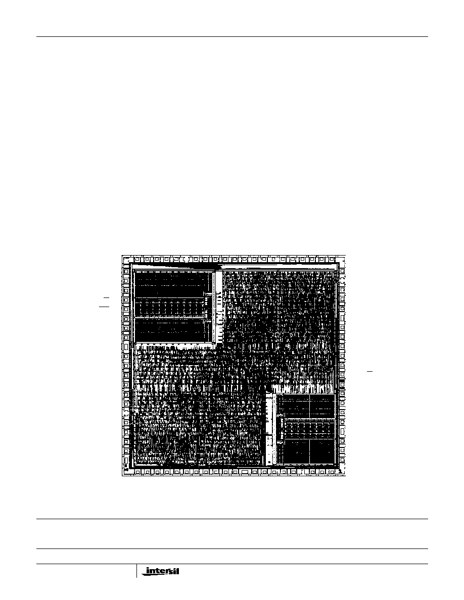
36
All Intersil semiconductor products are manufactured, assembled and tested under ISO9000 quality systems certification.
Intersil semiconductor products are sold by description only. Intersil Corporation reserves the right to make changes in circuit design and/or specifications at any time with-
out notice. Accordingly, the reader is cautioned to verify that data sheets are current before placing orders. Information furnished by Intersil is believed to be accurate and
reliable. However, no responsibility is assumed by Intersil or its subsidiaries for its use; nor for any infringements of patents or other rights of third parties which may result
from its use. No license is granted by implication or otherwise under any patent or patent rights of Intersil or its subsidiaries.
For information regarding Intersil Corporation and its products, see web site www.intersil.com
Die Characteristics
DIE DIMENSIONS:
364 mils x 371 mils x 21 mils
�
1mil
INTERFACE MATERIALS:
Glassivation:
Type: SiO
2
Thickness: 8k
�
�
1k
�
Top Metallization:
Type: Al/Si/Cu
Thickness: 7.5k
�
�
2k
�
Substrate:
TSOS5 CMOS,
Silicon on Sapphire
Backside Finish:
Silicon
ASSEMBLY RELATED INFORMATION:
Substrate Potential:
Unbiased (SOS)
ADDITIONAL INFORMATION:
Worst Case Current Density:
1.0 x 10
5
A/cm
2
Metallization Mask Layout
HS-RTX2010RH
MA16 (53)
MA15 (52)
MA14 (51)
VCC (50)
MA13 (49)
MA12 (48)
MA11 (47)
MA10 (46)
MA09 (45)
GND (44)
MA08 (43)
MA07 (42)
MA06 (41)
MA05 (40)
MA04 (39)
MA03 (38)
MA02 (37)
MA01 (36)
GD00 (35)
GD01 (34)
GD02 (33)
GND (32)
GD03 (31)
GD04 (30)
GD05 (29)
GD06 (28)
VCC (27)
GD07 (26)
GD08 (25)
GD09 (24)
GD10 (23)
GD11 (22)
GD12 (21)
GND (20)
GD13 (19)
GD14 (18)
GD15 (17)
GIO (16)
GR/W (15)
ICLK (14)
WAIT (13)
RESET (12)
(11) EI5
(10) EI4
(9) EI3
(8) EI2
(7) EI1
(6) VCC
(5) INTSUP
(4) NMI
(3) INT
A
(2) TCLK
(CQFP PIN 1) GA02
(84) GA01
(83) GA00
(82) MD15
(81) GND
(80) MD14
(79) MD13
(78) MD12
(77) MD11
(76) MD10
(75) MD09
(74) MD08
(73) VCC
(72) MD07
(71) MD06
(70) MD05
(69) GND
(68) MD04
(67) MD03
(66) MD02
(65) MD01
(64) MD00
(63) MR/W
(62) PCLK
(61) BOOT
(60) NEW
(59) UDS
(58) LDS
(57) GND
(56) MA19
(55) MA18
(54) MA17
HS-RTX2010RH