
1
CAUTION: These devices are sensitive to electrostatic discharge; follow proper IC Handling Procedures.
1-888-INTERSIL or 321-724-7143 | Copyright © Intersil Corporation 1999
ACTS541MS
Radiation Hardened Octal
Three-State Buffer/Line Driver
Pinouts
20 LEAD CERAMIC DUAL-IN-LINE
MIL-STD-1835 DESIGNATOR,
CDIP2-T20, LEAD FINISH C
TOP VIEW
20 LEAD CERAMIC FLATPACK
MIL-STD-1835 DESIGNATOR,
CDFP4-F20, LEAD FINISH C
TOP VIEW
11
12
13
14
15
16
17
18
20
19
10
9
8
7
6
5
4
3
2
1
OE1
A0
A1
A2
A3
A4
A6
A5
A7
GND
VCC
Y0
Y1
Y2
OE2
Y3
Y4
Y5
Y6
Y7
2
3
4
5
6
7
8
1
20
19
18
17
16
15
14
13
OE1
A0
A1
A2
A3
A4
A5
A6
9
10
12
11
A7
GND
VCC
Y0
Y1
Y2
OE2
Y3
Y4
Y5
Y6
Y7
Features
∑ Devices QML Qualified in Accordance with MIL-PRF-38535
∑ Detailed Electrical and Screening Requirements are Contained in
SMD# 5962-96726 and Intersil's QM Plan
∑ 1.25 Micron Radiation Hardened SOS CMOS
∑ Total Dose . . . . . . . . . . . . . . . . . . . . . . . . . . . . . . . . >300K RAD (Si)
∑ Single Event Upset (SEU) Immunity: <1 x 10
-10
Errors/Bit/Day
(Typ)
∑ SEU LET Threshold . . . . . . . . . . . . . . . . . . . . . . . >100 MEV-cm
2
/mg
∑ Dose Rate Upset . . . . . . . . . . . . . . . . >10
11
RAD (Si)/s, 20ns Pulse
∑ Dose Rate Survivability . . . . . . . . . . . >10
12
RAD (Si)/s, 20ns Pulse
∑ Latch-Up Free Under Any Conditions
∑ Military Temperature Range . . . . . . . . . . . . . . . . . . -55
o
C to +125
o
C
∑ Significant Power Reduction Compared to ALSTTL Logic
∑ DC Operating Voltage Range . . . . . . . . . . . . . . . . . . . . 4.5V to 5.5V
∑ Input Logic Levels
- VIL = 0.8V Max
- VIH = VCC/2 Min
∑ Input Current
1
µ
A at VOL, VOH
∑ Fast Propagation Delay . . . . . . . . . . . . . . . . 21ns (Max), 14ns (Typ)
Description
The Intersil ACTS541MS is a Radiation Hardened Octal Buffer/Line
Driver, with three-state outputs. The output enable pins OE1, OE2
control the three-state outputs. If either enable is high the output will be
in a high impedance state. For data output both enables must be low.
The ACTS541MS utilizes advanced CMOS/SOS technology to achieve
high-speed operation. This device is a member of a radiation hardened,
high-speed, CMOS/SOS Logic family.
The ACTS541MS is supplied in a 20 lead Ceramic Flatpack (K suffix) or
a Ceramic Dual-In-Line package (D suffix).
January 1996
Ordering Information
PART NUMBER
TEMPERATURE RANGE
SCREENING LEVEL
PACKAGE
5962F9672601VRC
-55
o
C to +125
o
C
MIL-PRF-38535 Class V
20 Lead SBDIP
5962F9672601VXC
-55
o
C to +125
o
C
MIL-PRF-38535 Class V
20 Lead Ceramic Flatpack
ACTS541D/Sample
25
o
C
Sample
20 Lead SBDIP
ACTS541K/Sample
25
o
C
Sample
20 Lead Ceramic Flatpack
ACTS541HMSR
25
o
C
Die
Die
Spec Number
518891
File Number
4094

2
ACTS541MS
Functional Diagram
TRUTH TABLE
INPUTS
OUTPUTS
OE1
OE2
An
Yn
L
L
H
H
L
L
L
L
H
X
X
Z
X
H
X
Z
NOTE: L = Low Logic Level, H = High Logic Level, Z = High Impedance
VCC
GND
Y0
18
VCC
GND
Y1
17
VCC
GND
Y2
16
VCC
GND
Y3
15
VCC
GND
Y4
14
VCC
GND
Y5
13
VCC
GND
Y6
12
VCC
GND
Y7
11
A0
2
A1
3
A2
4
A3
5
A4
6
A5
7
A6
8
A7
9
OE1
1
OE2
19
10
VCC
20
GND
Spec Number
518891
All Intersil semiconductor products are manufactured, assembled and tested under ISO9000 quality systems certification.
Intersil products are sold by description only. Intersil Corporation reserves the right to make changes in circuit design and/or specifications at any time without
notice. Accordingly, the reader is cautioned to verify that data sheets are current before placing orders. Information furnished by Intersil is believed to be accurate
and reliable. However, no responsibility is assumed by Intersil or its subsidiaries for its use; nor for any infringements of patents or other rights of third parties which
may result from its use. No license is granted by implication or otherwise under any patent or patent rights of Intersil or its subsidiaries.
For information regarding Intersil Corporation and its products, see web site http://www.intersil.com
3
ACTS541MS
Die Characteristics
DIE DIMENSIONS:
102 mils x 102 mils
2,600mm x 2,600mm
METALLIZATION:
Type: AlSi
Metal 1 Thickness: 7.125k
≈
±
1.125k
≈
Metal 2 Thickness: 9k
≈
±
1k
≈
GLASSIVATION:
Type: SiO
2
Thickness: 8k
≈
±
1k
≈
WORST CASE CURRENT DENSITY:
<2.0 x 10
5
A/cm
2
BOND PAD SIZE:
> 4.3 mils x 4.3 mils
> 110
µ
m x 110
µ
m
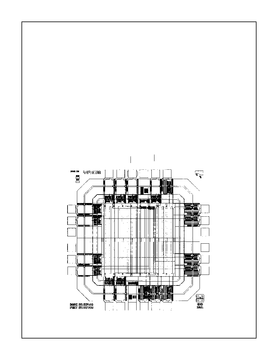
Metallization Mask Layout
ACTS541MS
(1)
OE1
(2) A0
(20) VCC
(16) Y2
GND (10)
Y7 (11)
Y6 (12)
NC
A2 (4)
A6 (8)
(14) Y4
(15) Y3
A3 (5)
NC
A4 (6)
NC
A5 (7)
A7 (9)
Y5 (13)
(17) Y1
NC
(3) A1
(18) Y
O
(19)
OE2
Spec Number
518891