1
August 1996
HS-1120RH
Radiation Hardened, Ultra High Speed
Current Feedback Amplifier with Offset Adjust
Features
∑ Electrically Screened to SMD 5962F9675601VPA
∑ MIL-PRF-38535 Class V Compliant
∑ Low Distortion (HD3, 30MHz) . . . . . . . . . . -84dBc (Typ)
∑ Wide -3dB Bandwidth . . . . . . . . . . . . . . . 850MHz (Typ)
∑ Very High Slew Rate . . . . . . . . . . . . . . . 2300V/
µ
s (Typ)
∑ Fast Settling (0.1%) . . . . . . . . . . . . . . . . . . . . 11ns (Typ)
∑ Excellent Gain Flatness (to 50MHz) . . . . . 0.05dB (Typ)
∑ High Output Current . . . . . . . . . . . . . . . . . . 65mA (Typ)
∑ Fast Overdrive Recovery. . . . . . . . . . . . . . . <10ns (Typ)
∑ Total Gamma Dose. . . . . . . . . . . . . . . . . . 300K RAD (Si)
∑ Latch Up . . . . . . . . . . . . . . . . . . . None (DI Technology)
Applications
∑ Video Switching and Routing
∑ Pulse and Video Amplifiers
∑ Wideband Amplifiers
∑ RF/IF Signal Processing
∑ Flash A/D Driver
∑ Imaging Systems
Description
The HS-1120RH is a radiation hardened, high speed,
wideband, fast settling current feedback amplifier. These
devices are QML approved and are processed and screened
in full compliance with MIL-PRF-38535. Built with Intersil'
proprietary, complementary bipolar UHF-1 (DI bonded
wafer) process, it is the fastest monolithic amplifier available
from any semiconductor manufacturer.
The HS-1120RH's wide bandwidth, fast settling
characteristic, and low output impedance, make this
amplifier ideal for driving fast A/D converters. Additionally, it
offers offset voltage nulling capabilities as described in the
"Offset Adjustment" section of this datasheet.
Component and composite video systems will also benefit
from this amplifier's performance, as indicated by the excel-
lent gain flatness, and 0.03%/0.05 Degree Differential
Gain/Phase specifications (R
L
= 75
).
Detailed electrical specifications are contained in SMD
5962F9675601VPA, available on the Intersil Website or
AnswerFAX systems (document #967560)
A Cross Reference Table is available on the Intersil Website
for conversion of Intersil Part Numbers to SMDs. The address
is (http://www.intersil.com/datasheets/smd/smd_xref.
html). SMD numbers must be used to order Radiation Hard-
ened Products.
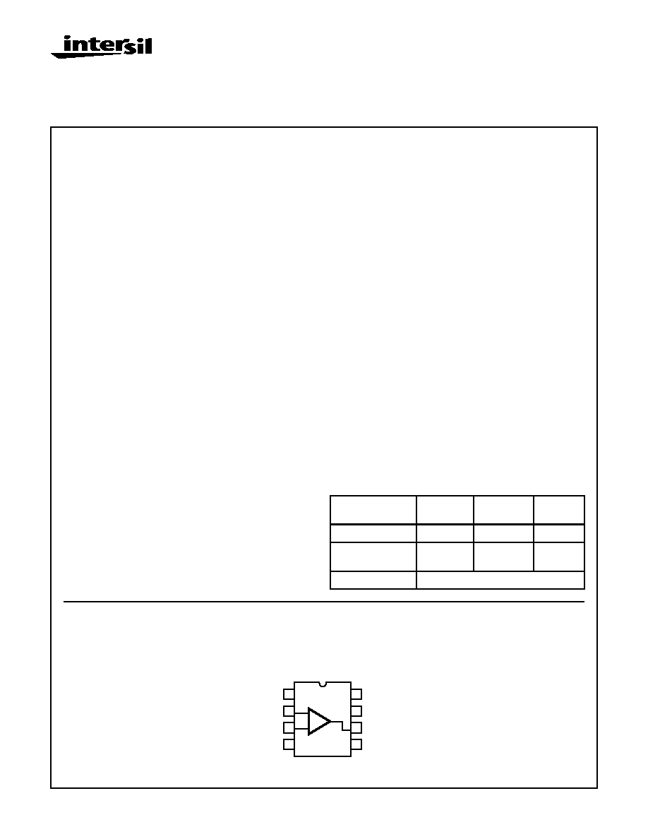
Pinout
HS-1120RH
MIL-STD-1835, GDIP1-T8
(CERDIP)
TOP VIEW
Ordering Information
PART NUMBER
TEMP.
RANGE (
o
C)
PACKAGE
PKG. NO.
5962F9675601VPA
-55 to 125
8 Ld CERDIP
GDIP1-T8
HFA1100IJ
(Sample)
-40 to 85
8 Ld CERDIP
F8.3A
HFA11XXEVAL
Evaluation Board
BAL
-IN
+IN
V-
1
2
3
4
8
7
6
5
NC
V+
OUT
BAL
-
+
File Number
4101.1
CAUTION: These devices are sensitive to electrostatic discharge; follow proper IC Handling Procedures.
1-888-INTERSIL or 321-724-7143 | Copyright © Intersil Corporation 1999

2
Application Information
Optimum Feedback Resistor
The enclosed plots of inverting and non-inverting frequency
response illustrate the performance of the HS-1120RH in
various gains. Although the bandwidth dependency on
closed loop gain isn't as severe as that of a voltage feedback
amplifier, there can be an appreciable decrease in
bandwidth at higher gains. This decrease may be minimized
by taking advantage of the current feedback amplifier's
unique relationship between bandwidth and R
F
. All current
feedback amplifiers require a feedback resistor, even for
unity gain applications, and R
F
, in conjunction with the
internal compensation capacitor, sets the dominant pole of
the frequency response. Thus, the amplifier's bandwidth is
inversely proportional to R
F
. The HS-1120RH design is
optimized for a 510
R
F
at a gain of +1. Decreasing R
F
in a
unity gain application decreases stability, resulting in
excessive peaking and overshoot. At higher gains the
amplifier is more stable, so R
F
can be decreased in a trade-
off of stability for bandwidth.
The table below lists recommended R
F
values for various
gains, and the expected bandwidth.
PC Board Layout
The frequency response of this amplifier depends greatly on
the amount of care taken in designing the PC board. The
use of low inductance components such as chip resis-
tors and chip capacitors is strongly recommended,
while a solid ground plane is a must!
Attention should be given to decoupling the power supplies.
A large value (10
µ
F) tantalum in parallel with a small value
(0.1
µ
F) chip capacitor works well in most cases.
Terminated microstrip signal lines are recommended at the
input and output of the device. Capacitance directly on the
output must be minimized, or isolated as discussed in the
next section.
Care must also be taken to minimize the capacitance to
ground seen by the amplifier's inverting input (-IN). The
larger this capacitance, the worse the gain peaking, resulting
in pulse overshoot and possible instability. To this end, it is
recommended that the ground plane be removed under
traces connected to -IN, and connections to -IN should be
kept as short as possible.
An example of a good high frequency layout is the Evalua-
tion Board shown in Figure 2.
Driving Capacitive Loads
Capacitive loads, such as an A/D input, or an improperly
terminated transmission line will degrade the amplifier's
phase margin resulting in frequency response peaking and
possible oscillations. In most cases, the oscillation can be
avoided by placing a resistor (R
S
) in series with the output
prior to the capacitance.
Figure 1 details starting points for the selection of this resis-
tor. The points on the curve indicate the R
S
and C
L
combina-
tions for the optimum bandwidth, stability, and settling time,
but experimental fine tuning is recommended. Picking a
point above or to the right of the curve yields an overdamped
response, while points below or left of the curve indicate
areas of underdamped performance.
R
S
and C
L
form a low pass network at the output, thus
limiting system bandwidth well below the amplifier band-
width of 850MHz. By decreasing R
S
as C
L
increases (as
illustrated in the curves), the maximum bandwidth is
obtained without sacrificing stability. Even so, bandwidth
does decrease as you move to the right along the curve.
For example, at A
V
= +1, R
S
= 50
, C
L
= 30pF, the overall
bandwidth is limited to 300MHz, and bandwidth drops to
100MHz at A
V
= +1, R
S
= 5
, C
L
= 340pF.
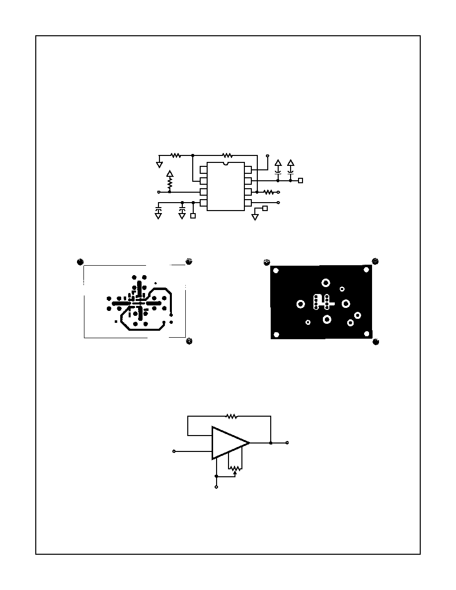
Evaluation Board
The performance of the HS-1120RH may be evaluated using
the HFA11XXEVAL Evaluation Board.
The layout and schematic of the board are shown in
Figure 2. To order evaluation boards, please contact your
local sales office.
Offset Adjustment
The output offset voltage of the HS-1120RH may be nulled via
connections to the BAL pins. Unlike a voltage feedback
amplifier, offset adjustment is accomplished by varying the sign
and/or magnitude of the inverting input bias current (-I
BIAS
).
With voltage feedback amplifiers, bias currents are matched
and bias current induced offset errors are nulled by matching
the impedances seen at the positive and negative inputs. Bias
GAIN
(A
CL
)
R
F
(
)
BANDWIDTH
(MHz)
-1
430
580
+1
510
850
+2
360
670
+5
150
520
+10
180
240
+19
270
125
R
S
(
)
LOAD CAPACITANCE (pF)
50
45
40
35
30
25
20
15
10
5
0
0
40
80
120
160
200
240
280
320
360
400
A
V
= +1
A
V
= +2
FIGURE 1. RECOMMENDED SERIES OUTPUT RESISTOR vs
LOAD CAPACITANCE
HS-1120RH
3
currents are uncorrelated on current feedback amplifiers, so
this technique is inappropriate.
-I
BIAS
flows through R
F
causing an output offset error.
Likewise, any change in -I
BIAS
forces a corresponding
change in output voltage, providing the capability for output
offset adjustment. By nulling -I
BIAS
to zero, the offset error
due to this current is eliminated. In addition, an adjustment
limit greater than the -I
BIAS
limit allows the user to null the
contributions from other error sources, such as V
IO
, or +IN
source impedance. For example, the excess adjust current
of 50
µ
A [I
BN
ADJ (Min) - I
BSN
(Max)] allows for the nulling of
an additional 26mV of output offset error (with R
F
= 510
) at
room temperature. The amount of adjustment is a function of
R
F
, so adjust range increases with increased R
F
. If allowed
by other considerations, such as bandwidth and noise, R
F
can be increased to provide more adjustment range.
The recommended offset adjustment circuit is shown in
Figure 3.
FIGURE 2A. SCHEMATIC
FIGURE 2B. TOP LAYOUT
FIGURE 2C. BOTTOM LAYOUT
FIGURE 2. EVALUATION BOARD SCHEMATIC AND LAYOUT
FIGURE 3. OFFSET VOLTAGE ADJUSTMENT CIRCUIT
1
2
3
4
8
7
6
5
+5V
10
µ
F
0.1
µ
F
V
H
50
GND
GND
R
1
-5V
0.1
µ
F
10
µ
F
50
IN
OUT
V
L
500
500
V
H
+IN
V
L
V+
GND
1
V-
OUT
HS-1120RH
-
+
2
3
4
510
6
10K
5
1
V
OUT
V-
V
IN
HS-1120RH
4
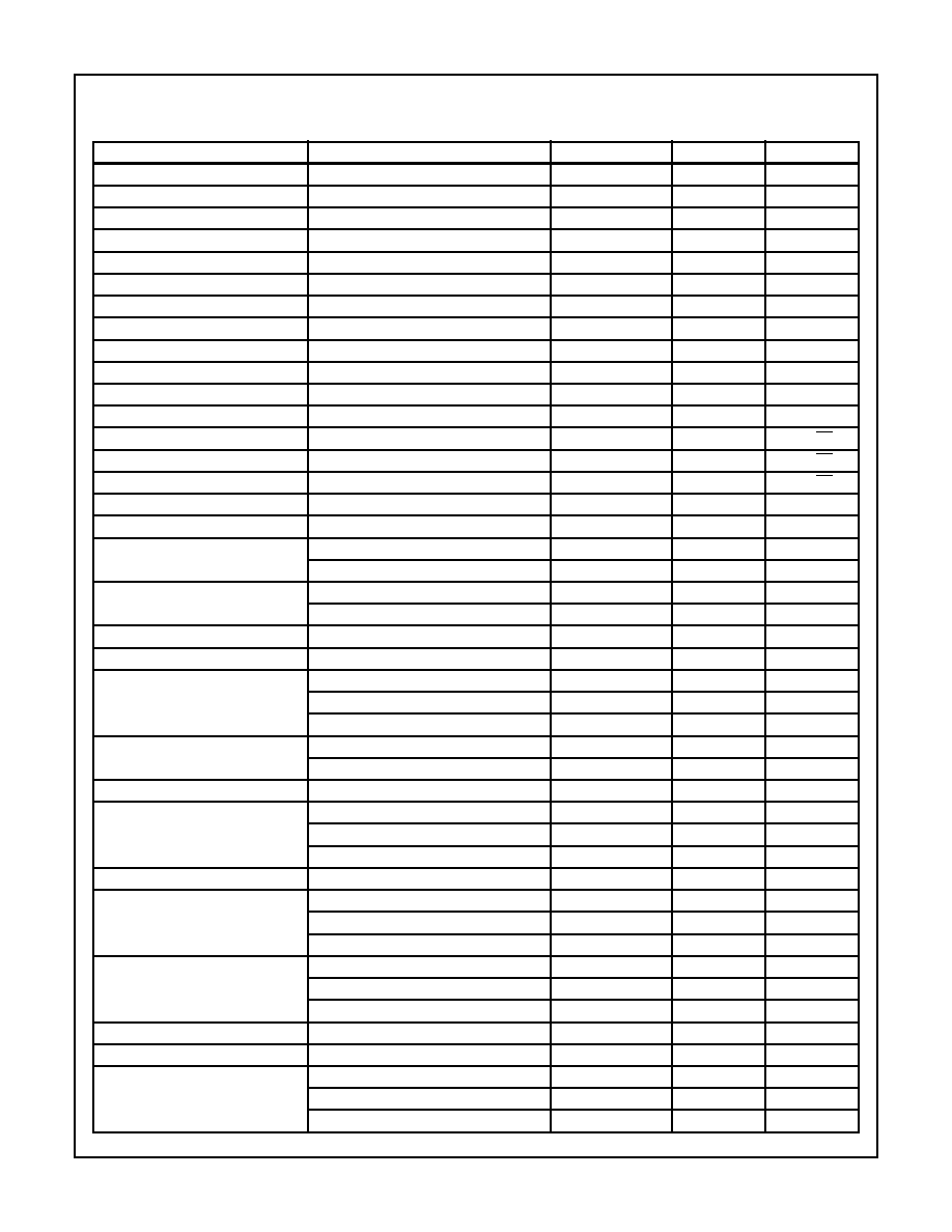
Typical Performance Characteristics
Device Characterized at: V
SUPPLY
=
±
5V, R
F
= 360
, A
V
= +2V/V, R
L
= 100
, Unless Otherwise Specified
PARAMETERS
CONDITIONS
TEMPERATURE
TYPICAL
UNITS
Input Offset Voltage (Note 1)
VCM = 0V
+25
o
C
2
mV
Average Offset Voltage Drift
Versus Temperature
Full
10
µ
V/
o
C
V
IO
CMRR
VCM =
±
2V
+25
o
C
46
dB
V
IO
PSRR
V
S
=
±
1.25V
+25
o
C
50
dB
+Input Current (Note 1)
VCM = 0V
+25
o
C
25
µ
A
Average +Input Current Drift
Versus Temperature
Full
40
nA/
o
C
-Input Current (Note 1)
VCM = 0V
+25
o
C
12
µ
A
Average -Input Current Drift
Versus Temperature
Full
40
nA/
o
C
-Input Current Adjust Range
VCM = 0V
+25
o
C
±
200
µ
A
+Input Resistance
VCM =
±
2V
+25
o
C
50
k
-Input Resistance
+25
o
C
16
Input Capacitance
+25
o
C
2.2
pF
Input Noise Voltage (Note 1)
f = 100kHz
+25
o
C
4
nV/
Hz
+Input Noise Current (Note 1)
f = 100kHz
+25
o
C
18
pA/
Hz
-Input Noise Current (Note 1)
f = 100kHz
+25
o
C
21
pA/
Hz
Input Common Mode Range
Full
±
3.0
V
Open Loop Transimpedance
A
V
= -1
+25
o
C
500
k
Output Voltage
A
V
= -1, R
L
= 100
+25
o
C
±
3.3
V
A
V
= -1, R
L
= 100
Full
±
3.0
V
Output Current (Note 1)
A
V
= -1, R
L
= 50
+25
o
C to +125
o
C
±
65
mA
A
V
= -1, R
L
= 50
-55
o
C to 0
o
C
±
50
mA
DC Closed Loop Output Resistance
+25
o
C
0.1
Quiescent Supply Current (Note 1)
R
L
= Open
Full
24
mA
-3dB Bandwidth (Note 1)
A
V
= -1, R
F
= 430
, V
OUT
= 200mV
P-P
+25
o
C
580
MHz
A
V
= +1, R
F
= 510
, V
OUT
= 200mV
P-P
+25
o
C
850
MHz
A
V
= +2, R
F
= 360
, V
OUT
= 200mV
P-P
+25
o
C
670
MHz
Slew Rate
A
V
= +1, R
F
= 510
, V
OUT
= 5V
P-P
+25
o
C
1500
V/
µ
s
A
V
= +2, V
OUT
= 5V
P-P
+25
o
C
2300
V/
µ
s
Full Power Bandwidth
V
OUT
= 5V
P-P
+25
o
C
220
MHz
Gain Flatness (Note 1)
To 30MHz, R
F
= 510
+25
o
C
±
0.014
dB
To 50MHz, R
F
= 510
+25
o
C
±
0.05
dB
To 100MHz, R
F
= 510
+25
o
C
±
0.14
dB
Linear Phase Deviation (Note 1)
To 100MHz, R
F
= 510
+25
o
C
±
0.6
Degrees
2nd Harmonic Distortion (Note 1)
30MHz, V
OUT
= 2V
P-P
+25
o
C
-55
dBc
50MHz, V
OUT
= 2V
P-P
+25
o
C
-49
dBc
100MHz, V
OUT
= 2V
P-P
+25
o
C
-44
dBc
3rd Harmonic Distortion (Note 1)
30MHz, V
OUT
= 2V
P-P
+25
o
C
-84
dBc
50MHz, V
OUT
= 2V
P-P
+25
o
C
-70
dBc
100MHz, V
OUT
= 2V
P-P
+25
o
C
-57
dBc
3rd Order Intercept (Note 1)
100MHz, R
F
= 510
+25
o
C
30
dBm
1dB Compression
100MHz, R
F
= 510
+25
o
C
20
dBm
Reverse Isolation (S
12
)
40MHz, R
F
= 510
+25
o
C
-70
dB
100MHz, R
F
= 510
+25
o
C
-60
dB
600MHz, R
F
= 510
+25
o
C
-32
dB
HS-1120RH

5
Rise and Fall Time
V
OUT
= 0.5V
P-P
+25
o
C
500
ps
V
OUT
= 2V
P-P
+25
o
C
800
ps
Overshoot (Note 1)
V
OUT
= 0.5V
P-P
, Input t
R
/t
F
= 550ps
+25
o
C
11
%
Settling Time (Note 1)
To 0.1%, V
OUT
= 2V to 0V, R
F
= 510
+25
o
C
11
ns
To 0.05%, V
OUT
= 2V to 0V, R
F
= 510
+25
o
C
19
ns
To 0.02%, V
OUT
= 2V to 0V, R
F
= 510
+25
o
C
34
ns
Differential Gain
A
V
= +2, R
L
= 75
, NTSC
+25
o
C
0.03
%
Differential Phase
A
V
= +2, R
L
= 75
, NTSC
+25
o
C
0.05
Degrees
Overdrive Recovery Time
R
F
= 510
, V
IN
= 5V
P-P
+25
o
C
7.5
ns
NOTE:
1. See Typical Performance Curve for more information.
Typical Performance Characteristics
(Continued)
Device Characterized at: V
SUPPLY
=
±
5V, R
F
= 360
, A
V
= +2V/V, R
L
= 100
, Unless Otherwise Specified (Continued)
PARAMETERS
CONDITIONS
TEMPERATURE
TYPICAL
UNITS
Typical Performance Curves
V
SUPPLY
=
±
5V, R
F
= 510
,
R
L
= 100
, T
A
= +25
o
C, Unless Otherwise Specified
FIGURE 4. SMALL SIGNAL PULSE RESPONSE (A
V
= +2)
FIGURE 5. LARGE SIGNAL PULSE RESPONSE (A
V
= +2)
FIGURE 6. NON-INVERTING FREQUENCY RESPONSE
(V
OUT
= 200mV
P-P
)
FIGURE 7. INVERTING FREQUENCY RESPONSE
(V
OUT
= 200mV
P-P
)
120
5ns/DIV.
90
60
30
0
-30
-60
-90
-120
OUTPUT V
O
L
T
A
GE (mV)
5ns/DIV.
OUTPUT V
O
L
T
A
GE (V)
1.2
0.9
0.6
0.3
0
-0.3
-0.6
-0.9
-1.2
FREQUENCY (MHz)
0
-3
-6
-9
-12
GAIN (dB) NORMALIZED
0.3
1
10
100
1K
0
-90
-180
-270
-360
PHASE
GAIN
A
V
= +1
A
V
= +1
A
V
= +11
A
V
= +2
A
V
= +6
A
V
= +11
A
V
= +2
A
V
= +6
PHASE (DEGREES)
FREQUENCY (MHz)
PHASE
GAIN
0
-3
-6
-9
-12
GAIN (dB) NORMALIZED
0.3
1
10
100
1K
180
90
0
-90
-180
A
V
= -1
A
V
= -1
A
V
= -20
A
V
= -5
A
V
= -10
A
V
= -20
A
V
= -5
A
V
= -10
PHASE (DEGREES)
HS-1120RH