1
File Number
4229.1
CAUTION: These devices are sensitive to electrostatic discharge; follow proper IC Handling Procedures.
1-888-INTERSIL or 321-724-7143 | Copyright © Intersil Corporation 1999
HS-1245RH
Radiation Hardened, Dual, High Speed,
Low Power Video Operational Amplifier
with Output Disable
The HS-1245RH is a radiation hardened dual high speed,
low power current feedback amplifier built with Intersil's
proprietary complementary bipolar UHF-1 (DI bonded wafer)
process. These devices are QML approved and are
processed and screened in full compliance with
MIL-PRF-38535.
This amplifier features individual TTL/CMOS compatible
disable controls, which when pulled low, reduce the supply
current and force the output into a high impedance state.
This allows easy implementation of simple, low power video
switching and routing systems. Component and composite
video systems also benefit from this op amp's excellent gain
flatness, and good differential gain and phase specifications.
Multiplexed A/D applications will also find the HS-1245RH
useful as the A/D driver/multiplexer.
Specifications for Rad Hard QML devices are controlled
by the Defense Supply Center in Columbus (DSCC). The
SMD numbers listed here must be used when ordering.
Detailed Electrical Specifications for these devices are
contained in SMD 5962-96832. A "hot-link" is provided
on our homepage for downloading.
www.intersil.com/spacedefense/space.asp
Features
∑ Electrically Screened to SMD # 5962-96832
∑ QML Qualified per MIL-PRF-38535 Requirements
∑ MIL-PRF-38535 Class V Compliant
∑ Low Supply Current . . . . . . . . . . . . . . . . . . . . 5.9mA (Typ)
∑ Wide -3dB Bandwidth. . . . . . . . . . . . . . . . . .530MHz (Typ)
∑ High Slew Rate. . . . . . . . . . . . . . . . . . . . . .1050V/
µ
s (Typ)
∑ Excellent Gain Flatness (to 50MHz) . . . . . .
±
0.11dB (Typ)
∑ Excellent Differential Gain . . . . . . . . . . . . . . . 0.02% (Typ)
∑ Excellent Differential Phase . . . . . . . . . 0.03 Degree (Typ)
∑ High Output Current . . . . . . . . . . . . . . . . . . . .60mA (Typ)
∑ Individual Output Enable/Disable
∑ Output Enable / Disable Time. . . . . . . . . 160ns/20ns (Typ)
∑ Total Gamma Dose. . . . . . . . . . . . . . . . . . . . 300kRAD(Si)
∑ Latch Up . . . . . . . . . . . . . . . . . . . . . None (DI Technology)
Applications
∑ Multiplexed Flash A/D Driver
∑ RGB Multiplexers and Preamps
∑ Video Switching and Routing
∑ Pulse and Video Amplifiers
∑ Wideband Amplifiers
∑ Hand Held and Miniaturized RF Equipment
∑ Battery Powered Communications
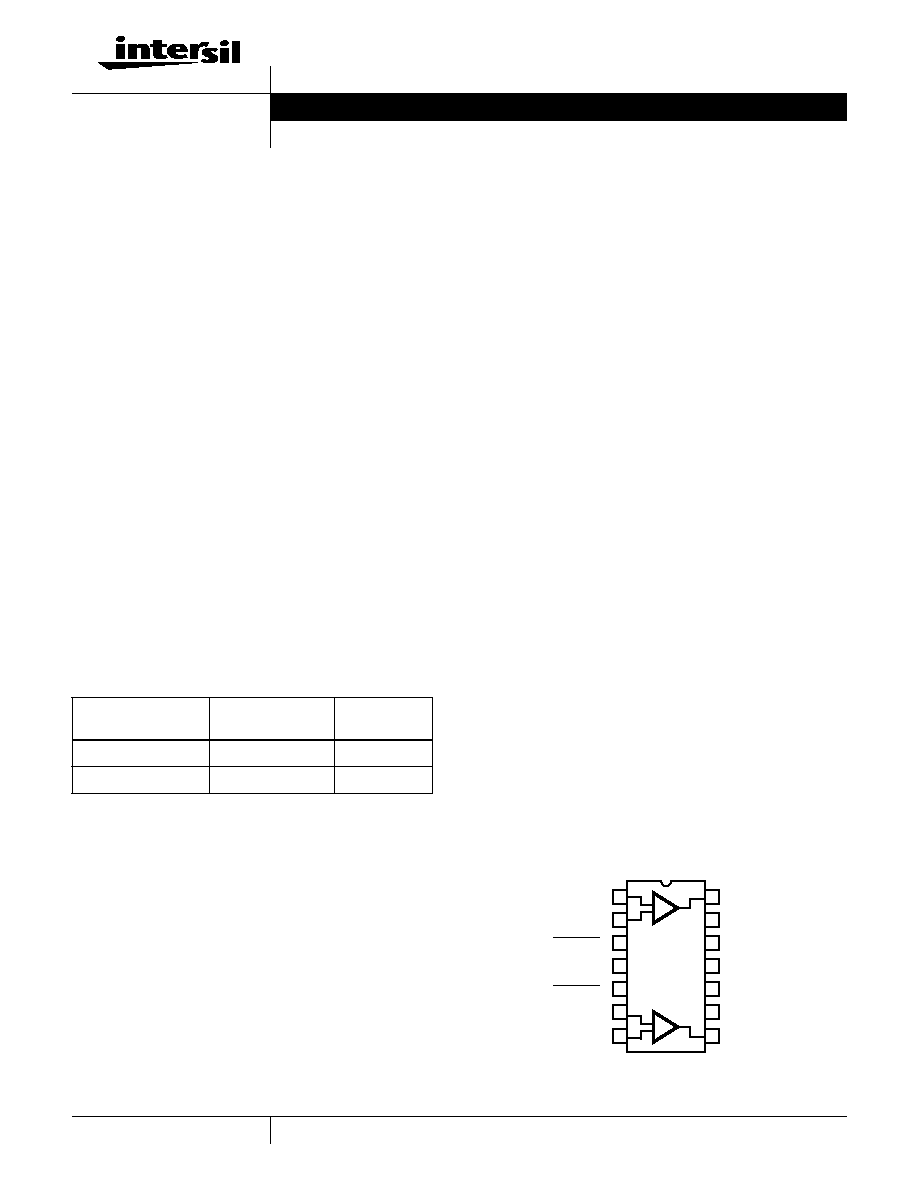
Pinout
HS-1245RH (CERDIP) GDIP1-T14
OR
HS-1245RH (SBDIP) CDIP2-T14
TOP VIEW
Ordering Information
ORDERING NUMBER
INTERNAL
MKT. NUMBER
TEMP. RANGE
(
o
C)
5962F9683201VCA
HS1-1245RH-Q
-55 to 125
5962F9683201VCC
HS1B-1245RH-Q
-55 to 125
1
2
3
4
5
6
7
14
13
12
11
10
9
8
-IN1
+IN1
DISABLE 1
DISABLE 2
+IN2
-IN2
OUT2
NC
NC
NC
OUT1
GND
V+
+
-
+
-
V-
Data Sheet
August 1999

2
Application Information
Optimum Feedback Resistor
Although a current feedback amplifier's bandwidth
dependency on closed loop gain isn't as severe as that of a
voltage feedback amplifier, there can be an appreciable
decrease in bandwidth at higher gains. This decrease may
be minimized by taking advantage of the current feedback
amplifier's unique relationship between bandwidth and R
F
.
All current feedback amplifiers require a feedback resistor,
even for unity gain applications, and R
F
, in conjunction with
the internal compensation capacitor, sets the dominant pole
of the frequency response. Thus, the amplifier's bandwidth is
inversely proportional to R
F
. The HS-1245RH design is
optimized for a 560
R
F
at a gain of +2. Decreasing R
F
decreases stability, resulting in excessive peaking and
overshoot (Note: Capacitive feedback will cause the same
problems due to the feedback impedance decrease at higher
frequencies). At higher gains the amplifier is more stable, so
R
F
can be decreased in a trade-off of stability for bandwidth.
The table below lists recommended R
F
values for various
gains, and the expected bandwidth. For good channel-to-
channel gain matching, it is recommended that all resistors
(termination as well as gain setting) be
±
1% tolerance or better.
Note that a series input resistor, on +IN, is required for a gain of
+1, to reduce gain peaking and increase stability.
Non-Inverting Input Source Impedance
For best operation, the D.C. source impedance looking out of
the non-inverting input should be
50
.
This is especially
important in inverting gain configurations where the non-
inverting input would normally be connected directly to GND.
Optional GND Pin for TTL Compatibility
The HS-1245RH derives an internal GND reference for the
digital circuitry as long as the power supplies are
symmetrical about GND. The GND reference is used to
ensure the TTL compatibility of the DISABLE inputs. With
symmetrical supplies the GND pin (Pin 12) may be floated,
or connected directly to GND. If asymmetrical supplies (e.g.
+10V, 0V) are utilized, and TTL compatibility is desired, the
GND pin must be connected to GND.
PC Board Layout
The frequency response of this amplifier depends greatly on
the amount of care taken in designing the PC board. The
use of low inductance components such as chip
resistors and chip capacitors is strongly recommended,
while a solid ground plane is a must!
Attention should be given to decoupling the power supplies.
A large value (10
µ
F) tantalum in parallel with a small value
(0.1
µ
F) chip capacitor works well in most cases.
Terminated microstrip signal lines are recommended at the
input and output of the device. Capacitance directly on the
output must be minimized, or isolated as discussed in the
next section.
Care must also be taken to minimize the capacitance to
ground seen by the amplifier's inverting input (-IN). The
larger this capacitance, the worse the gain peaking, resulting
in pulse overshoot and possible instability. To this end, it is
recommended that the ground plane be removed under
traces connected to -IN, and connections to -IN should be
kept as short as possible.
Driving Capacitive Loads
Capacitive loads, such as an A/D input, or an improperly
terminated transmission line will degrade the amplifier's
phase margin resulting in frequency response peaking and
possible oscillations. In most cases, the oscillation can be
avoided by placing a resistor (R
S
) in series with the output
prior to the capacitance.
Figure 1 details starting points for the selection of this
resistor. The points on the curve indicate the R
S
and C
L
combinations for the optimum bandwidth, stability, and
settling time, but experimental fine tuning is recommended.
Picking a point above or to the right of the curve yields an
overdamped response, while points below or left of the curve
indicate areas of underdamped performance.
R
S
and C
L
form a low pass network at the output, thus
limiting system bandwidth well below the amplifier
bandwidth of 290MHz (for A
V
= +1). By decreasing R
S
as
C
L
increases (as illustrated in the curves), the maximum
bandwidth is obtained without sacrificing stability. Even so,
bandwidth does decrease as you move to the right along
the curve. For example, at A
V
= +1, R
S
= 62
, C
L
= 40pF,
the overall bandwidth is limited to 180MHz, and bandwidth
drops to 70MHz at A
V
= +1, R
S
= 8
, C
L
= 400pF.
GAIN
(A
CL
)
R
F
(
)
BANDWIDTH
(MHz)
-1
510
230
+1
560 (+
R
S = 560
)
290
+2
560
530
0
100
200
300
400
0
10
20
30
40
50
LOAD CAPACITANCE (pF)
SERIES OUTPUT RESIST
ANCE (
)
A
V
= +1
A
V
= +2
150
250
350
50
FIGURE 1. RECOMMENDED SERIES OUTPUT RESISTOR vs
LOAD CAPACITANCE
HS-1245RH

4
All Intersil semiconductor products are manufactured, assembled and tested under ISO9000 quality systems certification.
Intersil semiconductor products are sold by description only. Intersil Corporation reserves the right to make changes in circuit design and/or specifications at any time with-
out notice. Accordingly, the reader is cautioned to verify that data sheets are current before placing orders. Information furnished by Intersil is believed to be accurate and
reliable. However, no responsibility is assumed by Intersil or its subsidiaries for its use; nor for any infringements of patents or other rights of third parties which may result
from its use. No license is granted by implication or otherwise under any patent or patent rights of Intersil or its subsidiaries.
For information regarding Intersil Corporation and its products, see web site http://www.intersil.com
Die Characteristics
DIE DIMENSIONS:
69 mils x 92 mils x 19 mils
±
1 mil
1750 x 2330 x 355
µ
m
±
25.4
µ
m
INTERFACE MATERIALS:
Glassivation:
Type: Nitride
Thickness: 4k
≈
±
0.5k
≈
Top Metallization:
Type: Metal 1: AICu(2%)/TiW
Type: Metal 2: AICu(2%)
Thickness: Metal 1: 8k
≈
±
0.4k
≈
Thickness: Metal 2: 16k
≈
±
0.8k
≈
Substrate:
UHF-1X, Bonded Wafer, DI
Backside Finish:
Silicon
ASSEMBLY RELATED INFORMATION:
Substrate Potential (Powered Up):
Floating
ADDITIONAL INFORMATION:
Worst Case Current Density:
< 2 x 10
5
A/cm
2
Transistor Count:
150
Metallization Mask Layout
HS-1245RH
NOTE: This is an optional GND pad. Users may set a GND reference, via this pad, to ensure the TTL compatibility of the DISABLE inputs when
using asymmetrical supplies (e.g., V+ = 10V, V- = 0V). See the "Application Information" section for details.
V-
OUT2
+IN1
-IN1
V+
V
L
+IN2
OUT1
-IN2
NC
NC
GND (NOTE)
DISABLE1
DISABLE2
V-
V-
HS-1245RH
