1
ACTS240T
High Reliability, Radiation Hardened Octal
Buffer/Line Driver, Three-State, Inverting
Intersil`s Satellite Applications Flow
TM
(SAF) devices are
fully tested and guaranteed to 100kRAD total dose. These
QML Class T devices are processed to a standard flow
intended to meet the cost and shorter lead-time needs of
large volume satellite manufacturers, while maintaining a
high level of reliability.
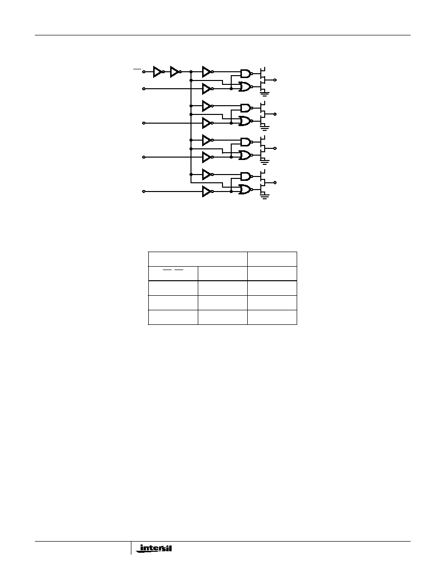
The Intersil ACTS240T is a Radiation Hardened High
Reliability, High-Speed CMOS/SOS Octal Buffer/Line Driver
with three-state outputs having two active low enable inputs.
Each enable input controls a set of four inverting buffer/line
drivers. A HIGH on the enable input places the outputs in a
high impedance state.
Specifications
Specifications for Rad Hard QML devices are controlled by
the Defense Supply Center in Columbus (DSCC). The SMD
numbers listed below must be used when ordering.
Detailed Electrical Specifications for the ACTS240T are
contained in SMD 5962-96717. A "hot-link" is provided from
our website for downloading.
www.intersil.com/spacedefense/newsafclasst.asp
Intersil`s Quality Management Plan (QM Plan), listing all
Class T screening operations, is also available on our
website.
www.intersil.com/quality/manuals.asp
Features
∑ QML Class T, Per MIL-PRF-38535
∑ Radiation Performance
- Gamma Dose (
) 1 x 10
5
RAD(Si)
- Latch-Up Free Under Any Conditions
- Single Event Upset (SEU) Immunity: <1 x 10
-10
Errors/Bit/Day (Typ)
- SEU LET Threshold . . . . . . . . . . . . .>100 MEV-cm
2
/mg
∑ 1.25 Micron Radiation Hardened SOS CMOS
∑ Significant Power Reduction Compared to ALSTTL Logic
∑ DC Operating Voltage Range . . . . . . . . . . . . 4.5V to 5.5V
∑ Input Logic Levels
- V
IL
= 0.8V Max
- V
IH
= V
CC/2
Min
∑ Fast Propagation Delay . . . . . . . 17.5ns (Max), 12ns (Typ)
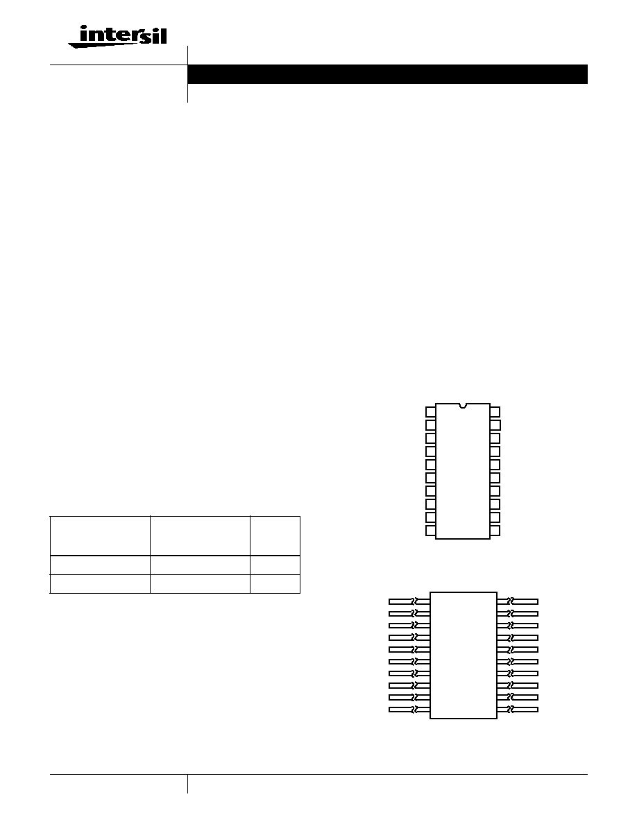
Pinouts
ACTS240T (SBDIP), CDIP2-T20
TOP VIEW
ACTS240T (FLATPACK), CDFP4-F20
TOP VIEW
Ordering Information
ORDERING
NUMBER
PART
NUMBER
TEMP.
RANGE
(
o
C)
5962R9671701TRC
ACTS240DTR
-55 to 125
5962R9671701TXC
ACTS240KTR
-55 to 125
NOTE:
Minimum order quantity for -T is 150 units through
distribution, or 450 units direct.
11
12
13
14
15
16
17
18
20
19
10
9
8
7
6
5
4
3
2
1
AEN
AI1
BO4
AI2
BO3
AI3
AI4
BO2
BO1
GND
V
CC
AO1
BI4
AO2
BEN
BI3
AO3
BI2
AO4
BI1
2
3
4
5
6
7
8
1
20
19
18
17
16
15
14
13
9
10
12
11
AEN
AI1
BO4
AI2
BO3
AI3
AI4
BO2
BO1
GND
V
CC
AO1
BI4
AO2
BEN
BI3
AO3
BI2
AO4
BI1
Data Sheet
July 1999
File Number
4610.1
CAUTION: These devices are sensitive to electrostatic discharge; follow proper IC Handling Procedures.
www.intersil.com or 407-727-9207
|
Copyright
©
Intersil Corporation 1999

3
All Intersil semiconductor products are manufactured, assembled and tested under ISO9000 quality systems certification.
Intersil semiconductor products are sold by description only. Intersil Corporation reserves the right to make changes in circuit design and/or specifications at any time with-
out notice. Accordingly, the reader is cautioned to verify that data sheets are current before placing orders. Information furnished by Intersil is believed to be accurate and
reliable. However, no responsibility is assumed by Intersil or its subsidiaries for its use; nor for any infringements of patents or other rights of third parties which may result
from its use. No license is granted by implication or otherwise under any patent or patent rights of Intersil or its subsidiaries.
For information regarding Intersil Corporation and its products, see web site http://www.intersil.com
Die Characteristics
DIE DIMENSIONS:
(2540
µ
m x 2540
µ
m x 533
µ
m
±
51
µ
m)
100 x 100 x 21mils
±
2mil
METALLIZATION:
Type: Al Si Cu
Thickness: 10.0k
≈
±
2k
≈
SUBSTRATE POTENTIAL:
Unbiased (Silicon on Sapphire)
Bond Pad #20 (V
CC
) First
Bond Pad #10 (Gnd) Uses Two Bond Wires
Bond Pad #20 (V
CC
) Uses Two Bond Wires
BACKSIDE FINISH:
Sapphire
PASSIVATION:
Type: Silox (S
i
O
2
)
Thickness: 8.0k
≈
±
1.0k
≈
WORST CASE CURRENT DENSITY:
< 2.0e5 A/cm
2
TRANSISTOR COUNT:
164
PROCESS:
CMOS SOS
Metallization Mask Layout
ACTS240T
BO4 (3)
AI2 (4)
BO3 (5)
AI3 (6)
BO2 (7)
AI4 (8)
V
CC
BO1 (9)
AO4 (12)
(13) BI2
(14) AO3
(15) BI3
(16) AO2
(17) BI4
(18) AO1
(20)
V
CC
(20)
AEN
(1)
AI1
(2)
BEN
(19)
(11)
BI1
(10)
GND
(10)
GND
ACTS240T