 | –≠–ª–µ–∫—Ç—Ä–æ–Ω–Ω—ã–π –∫–æ–º–ø–æ–Ω–µ–Ω—Ç: AD590 | –°–∫–∞—á–∞—Ç—å:  PDF PDF  ZIP ZIP |
12-3
August 1997
AD590
2-Wire, Current Output
Temperature Transducer
Features
∑ Linear Current Output . . . . . . . . . . . . . . . . . . . . 1
µ
A/
o
K
∑ Wide Temperature Range . . . . . . . . . . . -55
o
C to 150
o
C
∑ Two-Terminal Device Voltage In/Current Out
∑ Wide Power Supply Range . . . . . . . . . . . . . +4V to +30V
∑ Sensor Isolation From Case
∑ Low Cost
Description
The AD590 is an integrated-circuit temperature transducer
which produces an output current proportional to absolute tem-
perature. The device acts as a high impedance constant current
regulator, passing 1
µ
A/
o
K for supply voltages between +4V and
+30V. Laser trimming of the chip's thin film resistors is used to
calibrate the device to 298.2
µ
A output at 298.2
o
K (25
o
C).
The AD590 should be used in any temperature-sensing
application between -55
o
C to 150
o
C in which conventional
electrical temperature sensors are currently employed. The
inherent low cost of a monolithic integrated circuit combined
with the elimination of support circuitry makes the AD590 an
attractive alternative for many temperature measurement sit-
uations. Linearization circuitry, precision voltage amplifiers,
resistance measuring circuitry and cold junction compensa-
tion are not needed in applying the AD590. In the simplest
application, a resistor, a power source and any voltmeter can
be used to measure temperature.
In addition to temperature measurement, applications include
temperature compensation or correction of discrete
components, and biasing proportional to absolute temperature.
The AD590 is particularly useful in remote sensing applica-
tions. The device is insensitive to voltage drops over long
lines due to its high-impedance current output. Any well
insulated twisted pair is sufficient for operation hundreds of
feet from the receiving circuitry. The output characteristics
also make the AD590 easy to multiplex: the current can be
switched by a CMOS multiplexer or the supply voltage can
be switched by a logic gate output.
Ordering Information
PART
NUMBER
NON-
LINEARITY
(
o
C)
TEMP. RANGE
(
o
C)
PACKAGE
PKG.
NO.
AD590IH
±
3.0
-55 to 150
3 Ld Metal Can
(TO-52)
T3.A
AD590JH
±
1.5
-55 to 150
3 Ld Metal Can
(TO-52)
T3.A
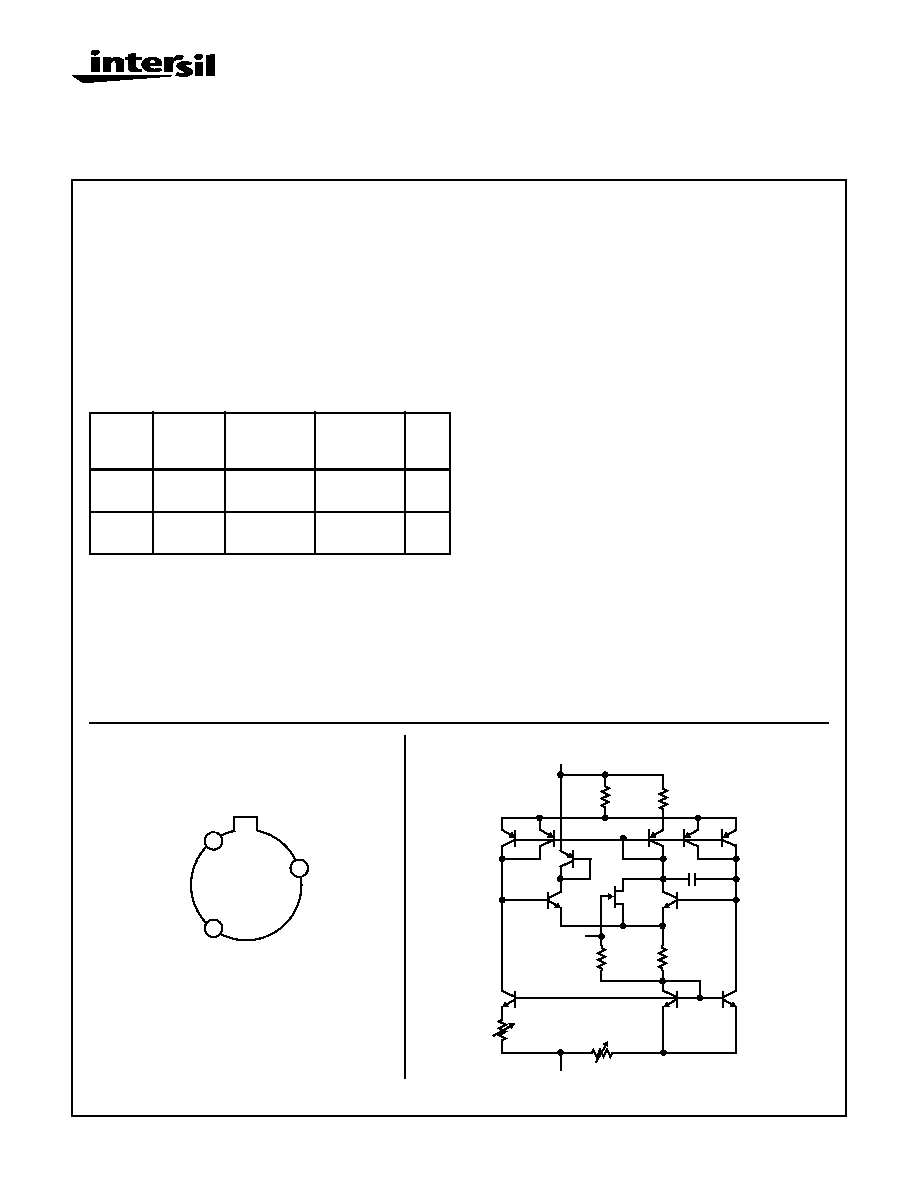
Pinout
AD590
(METAL CAN)
Functional Diagram
CASE
-
1
2
3
+
Q1
Q2
Q3
Q4
Q5
Q6
Q7
Q8
Q9
Q10
Q11
Q12
R1 260
R2 1040
C1 26pF
R3 5k
R4 11k
R6 820
R5 146
1
1
8
-
+
CHIP
SUBSTRATE
File Number
3171.1
CAUTION: These devices are sensitive to electrostatic discharge; follow proper IC Handling Procedures.
http://www.intersil.com or 407-727-9207
|
Copyright
©
Intersil Corporation 1999
12-4
Absolute Maximum Ratings
T
A
= 25
o
C
Thermal Information
Supply Forward Voltage (V+ to V-) . . . . . . . . . . . . . . . . . . . . . . +44V
Supply Reverse Voltage (V+ to V-) . . . . . . . . . . . . . . . . . . . . . . .-20V
Breakdown Voltage (Case to V+ to V-) . . . . . . . . . . . . . . . . . .
±
200V
Rated Performance Temperature Range TO-52. . . . -55
o
C to 150
o
C
Operating Conditions
Temperature Range . . . . . . . . . . . . . . . . . . . . . . . . . -55
o
C to 150
o
C
Thermal Resistance (Typical, Note 1)
JA
(
o
C/W)
JC
(
o
C/W)
Metal Can Package . . . . . . . . . . . . . . .
200
120
Maximum Junction Temperature (Metal Can Package) . . . . . . . 175
o
C
Maximum Storage Temperature Range . . . . . . . . . .-65
o
C to 150
o
C
Maximum Lead Temperature (Soldering 10s) . . . . . . . . . . . . . 300
o
C
CAUTION: Stresses above those listed in "Absolute Maximum Ratings" may cause permanent damage to the device. This is a stress only rating and operation
of the device at these or any other conditions above those indicated in the operational sections of this specification is not implied.
NOTE:
1.
JA
is measured with the component mounted on an evaluation PC board in free air.
Electrical Specifications
Typical Values at T
A
= 25
C, V+ = 5V, Unless Otherwise Specified
PARAMETER
TEST CONDITIONS
AD590I
AD590J
UNITS
Nominal Output Current at 2
o
C (298.2
o
K)
298.2
298.2
µ
A
Nominal Temperature Coefficient
1.0
1.0
µ
A/
o
K
Calibration Error at 25
o
C
Notes 1, 5
±
10.0 Max
±
5.0 Max
o
C
Absolute Error
-55
o
C to 150
o
C, Note 7
Without External Calibration Adjustment
±
20.0 Max
±
10.0 Max
o
C
With External Calibration Adjustment
±
5.8 Max
±
3.0 Max
o
C
Non-Linearity
Note 6
±
3.0 Max
±
1.5 Max
o
C
Repeatability
Notes 2, 6
±
0.1 Max
±
0.1 Max
o
C
Long Term Drift
Notes 3, 6
±
0.1 Max
±
0.1 Max
o
C/Month
Current Noise
40
40
pA
/
Hz
Power Supply Rejection
+4V < V+ < +5V
0.5
0.5
µ
A/V
+5V < V+ < +15V
0.2
0.2
µ
A/V
+15V < V+ < +30V
0.1
0.1
µ
A/V
Case Isolation to Either Lead
10
10
10
10
Effective Shunt Capacitance
100
100
pF
Electrical Turn-On Time
Note 1
20
20
µ
s
Reverse Bias Leakage Current
Note 4
10
10
pA
Power Supply Range
+4 to +30
+4 to +30
V
NOTES:
2. Does not include self heating effects.
3. Maximum deviation between 25
o
C reading after temperature cycling between -55
o
C and 150
o
C.
4. Conditions constant +5V, constant 125
o
C.
5. Leakage current doubles every 10
o
C.
6. Mechanical strain on package may disturb calibration of device.
7. Guaranteed but not tested.
8. -55
o
C Guaranteed by testing at 25
o
C and 150
o
C.
AD590

12-5
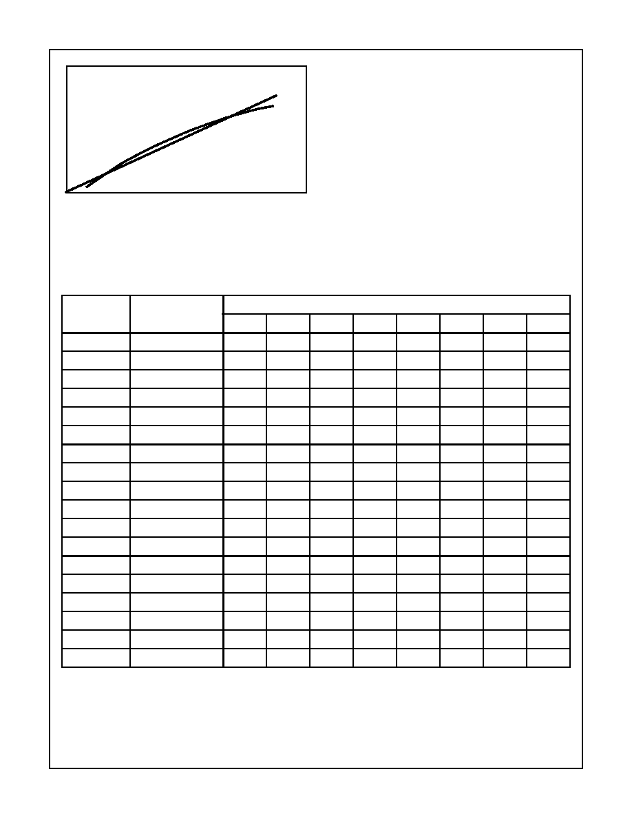
Trimming Out Errors
The ideal graph of current versus temperature for the AD590
is a straight line, but as Figure 1 shows, the actual shape is
slightly different. Since the sensor is limited to the range of
-55
o
C to 150
o
C, it is possible to optimize the accuracy by
trimming. Trimming also permits extracting maximum
performance from the lower-cost sensors.
The circuit of Figure 2 trims the slope of the AD590 output.
The effect of this is shown in Figure 3.
The circuit of Figure 4 trims both the slope and the offset.
This is shown in Figure 5. The diagrams are exaggerated to
show effects, but it should be clear that these trims can be
used to minimize errors over the whole range, or over any
selected part of the range. In fact, it is possible to adjust the
I-grade device to give less than 0.1
o
C error over the range
0
o
C to 90
o
C and less than 0.05
o
C error from 25
o
C to 60
o
C.
FIGURE 1. TRIMMING OUT ERRORS
I (
µ
A)
T (
o
K)
IDEAL
ACTUAL
(GREATLY
EXAGGERATED)
FIGURE 2. SLOPE TRIMMING
+5V
R 100
+
AD590
-
R = SLOPE
+
+
950
V
OUT
= 1mV/
o
K
FIGURE 3. EFFECT OF SLOPE TRIM
I (
µ
A)
T (
o
K)
IDEAL
ACTUAL
TRIMMED
FIGURE 4. SLOPE AND OFFSET TRIMMING
+10V
35.7k
R
1
2k
+
AD590
-
V
-
R
1
= OFFSET
R
2
= SLOPE
V
OUT
= 100mV/
o
C
97.6k
R
2
5k
FIGURE 5A. UNTRIMMED
FIGURE 5B. TRIM ONE: OFFSET
FIGURE 5C. TRIM TWO: SLOPE
AD590
12-6
Accuracy
Maximum errors over limited temperature spans, with
V
S
= +5V, are listed by device grade in the following tables.
The tables reflect the worst-case linearities, which invariably
occur at the extremities of the specified temperature range.
The trimming conditions for the data in the tables are shown
in Figure 2 and Figure 4.
All errors listed in the tables are
±
o
C. For example, if
±
1
o
C
maximum error is required over the 25
o
C to 75
o
C range (i.e.,
lowest temperature of 25
o
C and span of 50
o
C), then the
trimming of a J-grade device, using the single-trim circuit
(Figure 2), will result in output having the required accuracy
over the stated range. An I-grade device with two trims
(Figure 4) will have less than
±
0.2
o
C error. If the requirement
is for less than
±
1.4
o
C maximum error, from -25
o
C to 75
o
C
(100
o
C span from -25
o
C), it can be satisfied by an I-grade
device with two trims.
FIGURE 5D. TRIM THREE: OFFSET AGAIN
FIGURE 5. EFFECT OF SLOPE AND OFFSET TRIMMING
I Grade Maximum Errors (
o
C)
NUMBER OF
TRIMS
TEMPERATURE
SPAN (
o
C)
LOWEST TEMPERATURE IN SPAN (
o
C)
-55
-25
0
25
50
75
100
125
None
10
8.4
9.2
10.0
10.8
11.6
12.4
13.2
14.4
None
25
10.0
10.4
11.0
11.8
12.0
13.8
15.0
16.0
None
50
13.0
13.0
12.8
13.8
14.6
16.4
18.0
-
None
100
15.2
16.0
16.6
17.4
18.8
-
-
-
None
150
18.4
19.0
19.2
-
-
-
-
-
None
205
20.0
-
-
-
-
-
-
-
One
10
0.6
0.4
0.4
0.4
0.4
0.4
0.4
0.6
One
25
1.8
1.2
1.0
1.0
1.0
1.2
1.6
1.8
One
50
3.8
3.0
2.0
2.0
2.0
3.0
3.8
-
One
100
4.8
4.5
4.2
4.2
5.0
-
-
-
One
150
5.5
4.8
5.5
-
-
-
-
-
One
205
5.8
-
-
-
-
-
-
-
Two
10
0.3
0.2
0.1
(Note 9)
(Note 9)
0.1
0.2
0.3
Two
25
0.5
0.3
0.2
(Note 9)
0.1
0.2
0.3
0.5
Two
50
1.2
0.6
0.4
0.2
0.2
0.3
0.7
-
Two
100
1.8
1.4
1.0
2.0
2.5
-
-
-
Two
150
2.6
2.0
2.8
-
-
-
-
-
Two
205
3.0
-
-
-
-
-
-
-
NOTE:
9. Less than
±
0.05
o
C.
AD590

12-7
NOTES
1. Maximum errors over all ranges are guaranteed based on
the known behavior characteristic of the AD590.
2. For one-trim accuracy specifications, the 205
o
C span is
assumed to be trimmed at 25
o
C; for all other spans, it is
assumed that the device is trimmed at the midpoint.
3. For the 205
o
C span, it is assumed that the two-trim
temperatures are in the vicinity of 0
o
C and 140
o
C; for all
other spans, the specified trims are at the endpoints.
4. In precision applications, the actual errors encountered
are usually dependent upon sources of error which are
often overlooked in error budgets. These typically
include:
a. Trim error in the calibration technique used
b. Repeatability error
c. Long term drift errors
Trim Error is usually the largest error source. This error
arises from such causes as poor thermal coupling between
the device to be calibrated and the reference sensor; refer-
ence sensor errors; lack of adequate time for the device
being calibrated to settle to the final temperature; radically
different thermal resistances between the case and the sur-
roundings (R
CA
) when trimming and when applying the
device.
Repeatability Errors arise from a strain hysteresis of the
package. The magnitude of this error is solely a function of
the magnitude of the temperature span over which the
device is used. For example, thermal shocks between 0
o
C
and 100
o
C involve extremely low hysteresis and result in
repeatability errors of less than
±
0.05
o
C. When the thermal-
shock excursion is widened to -55
o
C to 150
o
C, the device
will typIcally exhibit a repeatability error of
±
0.05
o
C (
±
0.10
guaranteed maximum).
Long Term Drift Errors are related to the average operating
temperature and the magnitude of the thermal-shocks
experienced by the device. Extended use of the AD590 at
temperatures above 100
o
C typically results in long-term drift
of
±
0.03
o
C per month; the guaranteed maximum is
±
0.10
o
C
per month. Continuous operation at temperatures below
100
o
C induces no measurable drifts in the device. Besides
the effects of operating temperature, the severity of thermal
shocks incurred will also affect absolute stability. For
thermal-shock excursions less than 100
o
C, the drift is diffi-
cult to measure (<0.03
o
C). However, for 200
o
C excursions,
the device may drift by as much as
±
0.10
o
C after twenty
such shocks. If severe, quick shocks are necessary in the
application of the device, realistic simulated life tests are rec-
ommended for a thorough evaluation of the error introduced
by such shocks.
J Grade Maximum Errors (
o
C)
NUMBER OF
TRIMS
TEMPERATURE
SPAN (
o
C)
LOWEST TEMPERATURE IN SPAN (oC)
-55
-25
0
25
50
75
100
125
None
10
4.2
4.6
5.0
5.4
5.8
6.2
6.6
7.2
None
25
5.0
5.2
5.5
5.9
6.0
6.9
7.5
8.0
None
50
6.5
6.5
6.4
6.9
7.3
8.2
9.0
-
None
100
7.7
8.0
8.3
8.7
9.4
-
-
-
None
150
9.2
9.5
9.6
-
-
-
-
-
None
205
10.0
-
-
-
-
-
-
-
One
10
0.3
0.2
0.2
0.2
0.2
0.2
0.2
0.3
One
25
0.9
0.6
0.5
0.5
0.5
0.6
0.8
0.9
One
50
1.9
1.5
1.0
1.0
1.0
1.5
1.9
-
One
100
2.3
2.2
2.0
2.0
2.3
-
-
-
One
150
2.5
2.4
2.5
-
-
-
-
-
One
205
3.0
-
-
-
-
-
-
-
Two
10
0.1
(Note 10)
(Note 10)
(Note 10)
(Note 10)
(Note 10)
(Note 10)
0.1
Two
25
0.2
0.1
(Note 10)
(Note 10)
(Note 10)
(Note 10)
0.1
0.2
Two
50
0.4
0.2
0.1
(Note 10)
(Note 10)
0.1
0.2
(Note 10)
Two
100
0.7
0.5
0.3
0.7
1.0
-
-
-
Two
150
1.0
0.7
1.2
-
-
-
-
-
Two
205
1.6
-
-
-
-
-
-
-
NOTE:
10. Less than
±
0.05
o
C.
AD590