 | ÐлекÑÑоннÑй компоненÑ: AD7523K | СкаÑаÑÑ:  PDF PDF  ZIP ZIP |
AD7523, AD7533
1
TM
FN3105.2
AD7523, AD7533
8-Bit, 10-Bit Multiplying D/A Converters
The AD7523 and AD7533 are monolithic, low cost, high
performance, 8-bit and 10-bit accurate, multiplying digital-to-
analog converter (DAC), in a 16 pin DIP.
Intersil's thin film resistors on CMOS circuitry provide 10-bit
resolution (8-bit accuracy), with TTL/CMOS compatible
operation.
The AD7523 and AD7533's accurate four quadrant
multiplication, full input protection from damage due to static
discharge by clamps to V+ and GND, and very low power
dissipation make them very versatile converters.
Low noise audio gain controls, motor speed controls,
digitally controlled gain and digital attenuators are a few of
the wide range of applications of the AD7523 and AD7533.
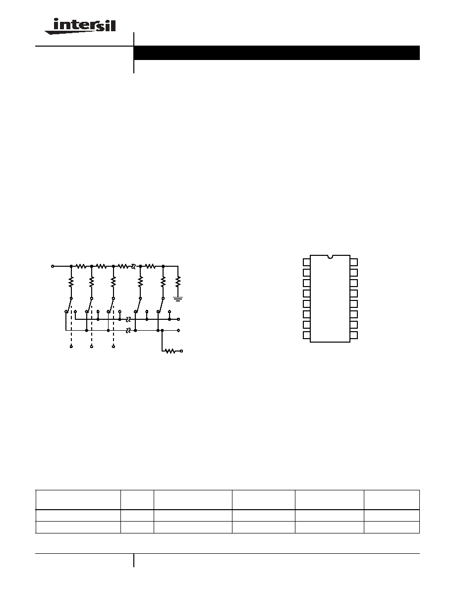
Functional Block Diagram
Features
· 8-Bit Linearity
· Low Gain and Linearity Temperature Coefficients
· Full Temperature Range Operation
· Static Discharge Input Protection
· TTL/CMOS Compatible
· Supply Range. . . . . . . . . . . . . . . . . . . . . . . . . +5V to +15V
· Fast Settling Time at 25
o
C. . . . . . . . . . . . . . 150ns (Max)
· Four Quadrant Multiplication
· AD7533 Direct AD7520 Equivalent
Pinout
AD7523, AD7533
(PDIP)
TOP VIEW
MSB
(4)
20k
(3)
BIT 3
BIT 2
V
REF IN
20k
20k
20k
20k
20k
10k
10k
10k
10k
SPDT
NMOS
10k
I
OUT2
(2)
I
OUT1
(1)
R
FEEDBACK
(15)
SWITCHES
(16)
(5)
(6)
NOTE: Switches shown for digital inputs "High"
14
15
16
9
13
12
11
10
1
2
3
4
5
7
6
8
I
OUT1
I
OUT2
GND
BIT 1 (MSB)
BIT 2
BIT 3
BIT 5
BIT 4
R
FEEDBACK
V+
NC/BIT 10
NC/BIT 9
BIT 8
BIT 7
BIT 6
V
REF IN
(NOTE)
(NOTE)
NOTE: NC for AD7523 only.
Ordering Information
PART NUMBER
NUMBER
OF BITS
LINEARITY (INL, DNL)
TEMP. RANGE (
o
C)
PACKAGE
PKG. NO.
AD7523JN
8
0.2% (8-Bit)
0 to 70
16 Ld PDIP
E16.3
AD7533JN
10
0.2% (8-Bit)
0 to 70
16 Ld PDIP
E16.3
Data Sheet
January 2001
CAUTION: These devices are sensitive to electrostatic discharge; follow proper IC Handling Procedures.
1-888-INTERSIL or 321-724-7143
|
Intersil (and design) is a trademark of Intersil Americas Inc.
Copyright © Intersil Americas Inc. 2002. All Rights Reserved
2
Absolute Maximum Ratings
Thermal Information
Supply Voltage (V+ to GND) . . . . . . . . . . . . . . . . . . . . . . . . . . .+17V
V
REF
. . . . . . . . . . . . . . . . . . . . . . . . . . . . . . . . . . . . . . . . . . . .
±
25V
Digital Input Voltage Range . . . . . . . . . . . . . . . . . . . . . . . V+ to GND
Output Voltage Compliance. . . . . . . . . . . . . . . . . . . . . -100mV to V+
Operating Conditions
Temperature Range. . . . . . . . . . . . . . . . . . . . . . . . . . . . 0
o
C to 70
o
C
Thermal Resistance (Typical, Note 1)
JA
(
o
C/W)
PDIP Package . . . . . . . . . . . . . . . . . . . . . . . . . . . . .
90
Maximum Junction Temperature (Plastic Package) . . . . . . . .150
o
C
Maximum Storage Temperature . . . . . . . . . . . . . . . -65
o
C to 150
o
C
Maximum Lead Temperature (Soldering 10s) . . . . . . . . . . . . . 300
o
C
CAUTION: Stresses above those listed in "Absolute Maximum Ratings" may cause permanent damage to the device. This is a stress only rating and operation of the
device at these or any other conditions above those indicated in the operational sections of this specification is not implied.
NOTE:
1.
JA
is measured with the component mounted on a low effective thermal conductivity test board in free air. See Tech Brief TB379 for details.
Electrical Specifications
V+ = +15V, V
REF
= +10V, V
OUT1
= V
OUT2
= 0V, Unless Otherwise Specified
PARAMETER
TEST CONDITIONS
AD7523
AD7533
UNITS
T
A
25
o
C
T
A
MIN-MAX
T
A
25
o
C
T
A
MIN-MAX
MIN
MAX
MIN
MAX
MIN
MAX
MIN
MAX
SYSTEM PERFORMANCE
Resolution
8
-
8
-
10
-
10
-
Bits
Nonlinearity
-10V
V
REF
+10V,
V
OUT1
= V
OUT2
= 0V
(Notes 2, 3, 6)
-
±
0.2
-
±
0.2
-
±
0.2
-
±
0.2
% of
FSR
Monotonicity
Guaranteed
Guaranteed
Gain Error
All Digital Inputs High (Note 3)
-
±
1.5
-
±
1.8
-
±
1.4
-
±
1.8
% of
FSR
Nonlinearity Tempco
-10V
V
REF
+ 10V
(Notes 3, 4)
-
±
2
-
±
2
-
±
2
-
±
2
ppm of
FSR/
o
C
Gain Error Tempco
-
±
10
-
±
10
-
±
10
-
±
10
ppm of
FSR/
o
C
Output Leakage Current
(Either Output)
V
OUT1
= V
OUT2
= 0
-
±
50
-
±
200
-
±
50
-
±
200
nA
DYNAMIC CHARACTERISTICS
Power Supply Rejection
V+ = 14.0V to 15.0V (Note 3)
-
±
0.02
-
±
0.03
-
±
0.005
-
±
0.008
% of
FSR/%
of
V+
Output Current Settling Time
To 0.2% of FSR,
R
L
= 100
(Note 4)
-
150
-
200
-
600
-
800
ns
Feedthrough Error
V
REF
= 20V
P-P
, 200kHz
Sine Wave, All Digital
Inputs Low (Note 4)
-
±
1/2
-
±
1
-
±
0.05
-
±
0.1
LSB
REFERENCE INPUTS
Input Resistance (Pin 15)
All Digital Inputs High I
OUT1
at Ground (Note 4)
5
-
5
-
5
-
5
-
k
-
20
-
20
-
20
-
20
k
Temperature Coefficient
-
-500
-
-500
-
-300
-
-300
ppm/
C
AD7523, AD7533
3
Definition of Terms
Nonlinearity: Error contributed by deviation of the DAC
transfer function from a "best straight line" through the actual
plot of transfer function. Normally expressed as a
percentage of full scale range or in (sub)multiples of 1 LSB.
Resolution: It is addressing the smallest distinct analog
output change that a D/A converter can produce. It is
commonly expressed as the number of converter bits. A
converter with resolution of n bits can resolve output changes
of 2
-N
of the full-scale range, e.g., 2
-N
V
REF
for a unipolar
conversion. Resolution by no means implies linearity.
Settling Time: Time required for the output of a DAC to
settle to within specified error band around its final value
(e.g.,
1
/
2
LSB) for a given digital input change, i.e., all digital
inputs LOW to HIGH and HIGH to LOW.
Gain Error: The difference between actual and ideal analog
output values at full-scale range, i.e., all digital inputs at
HIGH state. It is expressed as a percentage of full scale
range or in (sub)multiples of 1 LSB.
Feedthrough Error: Error caused by capacitive coupling
from V
REF
to I
OUT1
with all digital inputs LOW.
Output Capacitance: Capacitance from I
OUT1
, and I
OUT2
terminals to ground.
Output Leakage Current: Current which appears on
I
OUT1
, terminal when all digital inputs are LOW or on I
OUT2
terminal when all digital inputs are HIGH.
For further information on the use of this device, see the
following Application Notes:
ANALOG OUTPUT
Output Capacitance
C
OUT1
All Digital Inputs High (Note 4)
-
100
-
100
-
100
-
100
pF
C
OUT2
-
30
-
30
-
35
-
35
pF
C
OUT1
All Digital Inputs Low (Note 4)
-
30
-
30
-
35
-
35
pF
C
OUT2
-
100
-
100
-
100
-
100
pF
DIGITAL INPUTS
Low State Threshold, V
IL
-
0.8
-
0.8
-
0.8
-
0.8
V
High State Threshold, V
IH
2,4
-
2,4
-
2.4
-
2.4
-
V
Input Current (Low or High), I
IL
, I
IH
V
IN
= 0V or + 15V
-
±
1
-
±
1
-
±
1
-
±
1
µ
A
Input Coding
See Tables 1 through 3
Binary/Offset Binary
Binary/Offset Binary
Input Capacitance
(Note 4)
-
4
-
4
-
4
-
4
pF
POWER SUPPLY CHARACTERISTICS
Power Supply Voltage Range
(Note 6)
+5 to +16
+5 to +16
V
I+
All Digital Inputs High or Low
(Excluding Ladder Network)
-
2
-
2.5
-
2
-
2.5
mA
NOTES:
2. Full Scale Range (FSR) is 10V for unipolar and
±
10V for bipolar modes.
3. Using internal feedback resistor, R
FEEDBACK
.
4. Guaranteed by design or characterization and not production tested.
5. Accuracy not guaranteed unless outputs at ground potential.
6. Accuracy is tested and guaranteed at V+ = +15V, only.
Electrical Specifications
V+ = +15V, V
REF
= +10V, V
OUT1
= V
OUT2
= 0V, Unless Otherwise Specified (Continued)
PARAMETER
TEST CONDITIONS
AD7523
AD7533
UNITS
T
A
25
o
C
T
A
MIN-MAX
T
A
25
o
C
T
A
MIN-MAX
MIN
MAX
MIN
MAX
MIN
MAX
MIN
MAX
Application Notes
NOTE #
DESCRIPTION
AN002
"Principles of Data Acquisition and Conversion"
AN018
"Do's and Don'ts of Applying A/D Converters"
AN042
"Interpretation of Data Conversion Accuracy
Specifications"
AD7523, AD7533
4
Detailed Description
The AD7523 and AD7533 are monolithic multiplying D/A
converters. A highly stable thin film R-2R resistor ladder
network and NMOS SPDT switches form the basis of the
converter circuit, CMOS level shifters permit low power
TTL/CMOS compatible operation. An external voltage or
current reference and an operational amplifier are all that is
required for most voltage output applications.
A simplified equivalent circuit of the DAC is shown in the
Functional Diagram. The NMOS SPDT switches steer the
ladder leg currents between I
OUT1
and I
OUT2
buses which
must be held at ground potential. This configuration
maintains a constant current in each ladder leg independent
of the input code.
Converter errors are further reduced by using separate
metal interconnections between the major bits and the
outputs. Use of high threshold switches reduce offset
(leakage) errors to a negligible level.
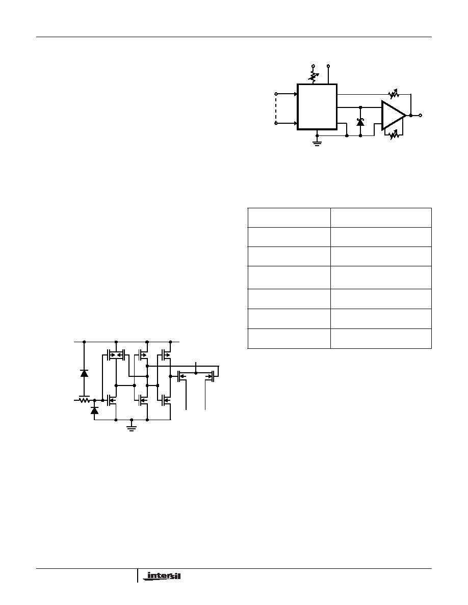
The level shifter circuits are comprised of three inverters with
positive feedback from the output of the second to the first,
see Figure 1. This configuration results in TTL/CMOS
compatible operation over the full military temperature
range. With the ladder SPDT switches driven by the level
shifter, each switch is binarily weighted for an ON resistance
proportional to the respective ladder leg current. This
assures a constant voltage drop across each switch,
creating equipotential terminations for the 2R ladder
resistors and high accurate leg currents.
Typical Applications
Unipolar Binary Operation - AD7523 (8-Bit DAC)
The circuit configuration for operating the AD7523 in
unipolar mode is shown in Figure 2. With positive and
negative V
REF
values the circuit is capable of 2-Quadrant
multiplication. The "Digital Input Code/Analog Output Value"
table for unipolar mode is given in Table 1.
Zero Offset Adjustment
1. Connect all digital inputs to GND.
2. Adjust the offset zero adjust trimpot of the output
operational amplifier for 0V
±
1mV (Max) at V
OUT
.
Gain Adjustment
1. Connect all digital inputs to V+.
2. Monitor V
OUT
for a -V
REF
(1
1
/
2
8
) reading.
3. To increase V
OUT
, connect a series resistor, R2, (0
to
250
) in the I
OUT1
amplifier feedback loop.
4. To decrease V
OUT
, connect a series resistor, R1, (0
to
250
) between the reference voltage and the V
REF
terminal.
Unipolar Binary Operation - AD7533 (10-Bit DAC)
The circuit configuration for operating the AD7533 in
unipolar mode is shown in Figure 2. With positive and
negative V
REF
values the circuit is capable of 2-Quadrant
multiplication. The "Digital Input Code/Analog Output Value"
table for unipolar mode is given in Table 2.
V+
TTL/
CMOS INPUT
1 3
4
5
6
7
2
8
9
TO LADDER
I
OUT2
I
OUT1
FIGURE 1. CMOS SWITCH
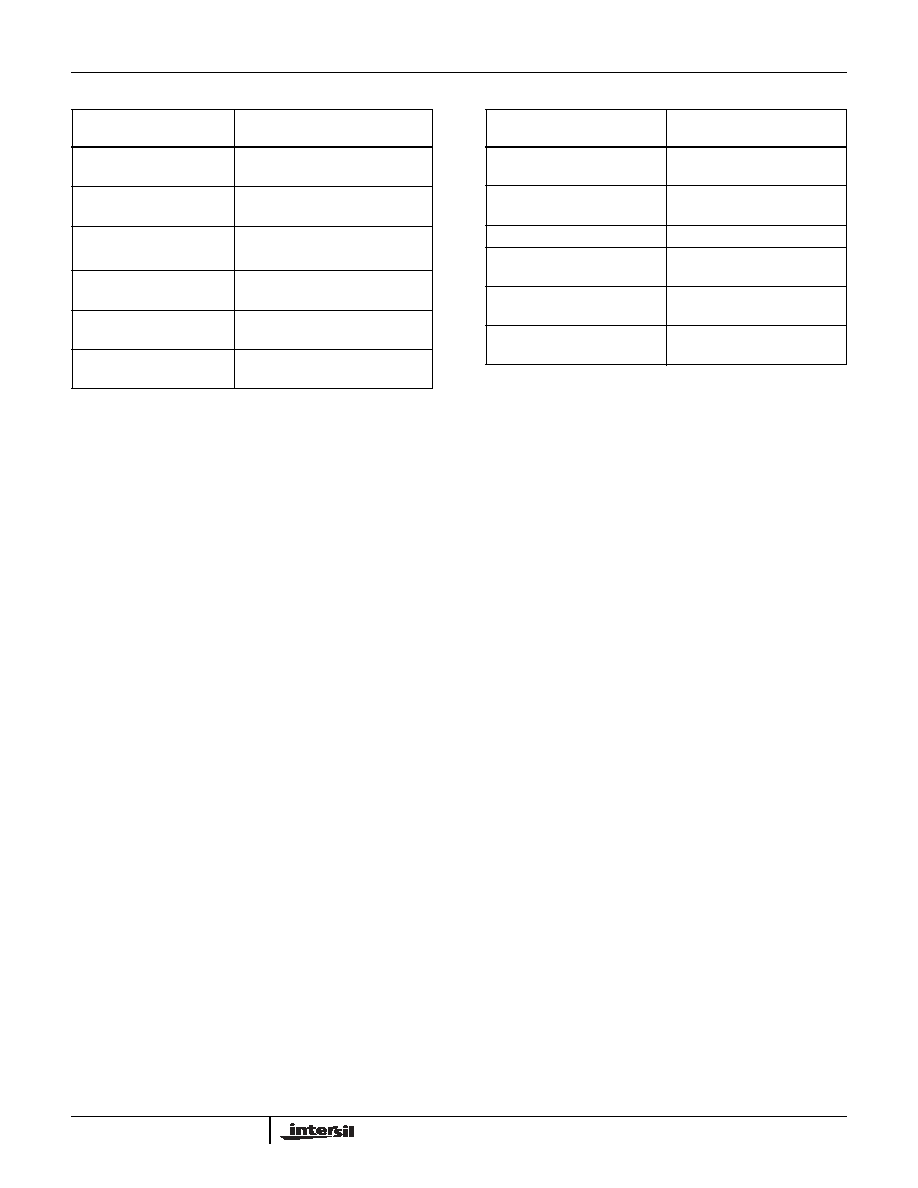
TABLE 1. UNlPOLAR BINARY CODE - AD7523
DIGITAL INPUT
MSB LSB
ANALOG OUTPUT (V
OUT
)
11111111
10000001
10000000
01111111
00000001
00000000
NOTES:
9.
.
15
16
1
4
11
3
2
AD7523/
MSB
LSB
14
+15V
V
REF
GND
OUT1
OUT2
6
V
OUT
-
+
R
FEEDBACK
DATA
INPUTS
AD7533
±
10V
R2
CR1
NOTES:
7. R1 and R2 used only if gain adjustment is required.
8. CR1 protects AD7523 and AD7533 against negative transients.
FIGURE 2. UNIPOLAR BINARY OPERATION
R1
VREF
255
256
----------
VREF
129
256
----------
VREF
128
256
----------
VREF
2
-----------------
=
VREF
127
256
----------
VREF
1
256
----------
VREF
0
256
----------
0
=
1 LSB
2
8
(
)
V
REF
(
)
1
256
----------
V
REF
(
)
=
=
AD7523, AD7533
5
Zero Offset Adjustment
5. Connect all digital inputs to GND.
6. Adjust the offset zero adjust trimpot of the output
operational amplifier for 0V
±
1mV (Max) at V
OUT
.
Gain Adjustment
1. Connect all digital inputs to V+.
2. Monitor V
OUT
for a -V
REF
(1 - 1/2
10
) reading.
3. To increase V
OUT
, connect a series resistor, R2, (0
to
250
) in the I
OUT1
amplifier feedback loop.
4. To decrease V
OUT
, connect a series resistor, R1, (0
to
250
) between the reference voltage and the V
REF
terminal.
Bipolar (Offset Binary) Operation - AD7523
The circuit configuration for operating the AD7523 in the
bipolar mode is given in Figure 3. Using offset binary digital
input codes and positive and negative reference voltage
values, Four-Quadrant multiplication can be realized. The
"Digital Input Code/Analog Output Value" table for bipolar
mode is given in Table 3.)
A "Logic 1" input at any digital input forces the corresponding
ladder switch to steer the bit current to I
OUT1
bus. A "Logic
0" input forces the bit current to I
OUT2
bus. For any code the
I
OUT1
and I
OUT2
bus currents are complements of one
another. The current amplifier at I
OUT2
changes the polarity
of I
OUT2
current and the transconductance amplifier at I
OUT
output sums the two currents. This configuration doubles the
output range. The difference current resulting at zero offset
binary code, (MSB = "Logic 1", all other bits = "Logic 0"), is
corrected by using an external resistor, (10M
), from V
REF
to I
OUT2
(Figure 3).
Offset Adjustment
1. Adjust V
REF
to approximately +10V.
2. Connect all digital inputs to "Logic 1".
3. Adjust I
OUT2
amplifier offset adjust trimpot for 0V
±
1mV at
I
OUT2
amplifier output.
4. Connect MSB (Bit 1) to "Logic 1" and all other bits to
"Logic 0".
5. Adjust I
OUT1
amplifier offset adjust trimpot for 0V
±
1mV
at V
OUT
.
Gain Adjustment
1. Connect all digital inputs to V+.
2. Monitor V
OUT
for a -V
REF
(1
1
/
2
8
) volts reading.
3. To increase V
OUT
, connect a series resistor, R2, of up to
250
between V
OUT
and R
FEEDBACK
.
4. To decrease V
OUT
, connect a series resistor, R1, of up to
250
between the reference voltage and the V
REF
terminal.
Bipolar (Offset Binary) Operation - AD7533
The circuit configuration for operating the AD7533 in the
bipolar mode is given in Figure 3. Using offset binary digital
input codes and positive and negative reference voltage
values, 4-Quadrant multiplication can be realized. The
"Digital Input Code/Analog Output Value" table for bipolar
mode is given in Table 4.
A "Logic 1" input at any digital input forces the
corresponding ladder switch to steer the bit current to
I
OUT1
bus. A "Logic 0" input forces the bit current to I
OUT2
bus. For any code the I
OUT1
and I
OUT2
bus currents are
complements of one another. The current amplifier at
I
OUT2
changes the polarity of I
OUT2
current and the
transconductance amplifier at I
OUT1
output sums the two
currents. This configuration doubles the output range. The
difference current resulting at zero offset binary code,
(MSB = "Logic 1", all other bits = "Logic 0"), is corrected by
using an external resistor, (10M
), from V
REF
to I
OUT2
.
TABLE 2. UNlPOLAR BINARY CODE - AD7533
DIGITAL INPUT
MSB LSB
(NOTE 10)
NOMINAL ANALOG OUTPUT
1111111111
1000000001
1000000000
0111111111
0000000001
0000000000
NOTES:
10. V
OUT
as shown in Figure 2.
11. Nominal Full Scale for the circuit of Figure 2 is given by:
.
12. Nominal LSB magnitude for the circuit of Figure 2 is given by:
.
V
REF
1023
1024
-------------
V
REF
513
1024
-------------
VREF
512
1024
-------------
V
REF
2
---------------
=
V
REF
511
1024
-------------
V
REF
1
1024
-------------
V
REF
0
1024
-------------
0
=
FS
VREF
1023
1024
-------------
=
LSB
VREF
1
1024
-------------
=
TABLE 3. BlPOLAR (OFFSET BINARY) CODE - AD7523
DIGITAL INPUT
MSB LSB
ANALOG OUTPUT
11111111
10000001
10000000
0
01111111
00000001
00000000
NOTES:
13.
.
VREF
127
128
----------
VREF
1
128
----------
+VREF
1
128
----------
+VREF
127
128
----------
+VREF
128
128
----------
1 LSB
2
7
(
)
VREF
(
)
1
128
----------
VREF
(
)
=
=
AD7523, AD7533