 | –≠–ª–µ–∫—Ç—Ä–æ–Ω–Ω—ã–π –∫–æ–º–ø–æ–Ω–µ–Ω—Ç: AD7530 | –°–∫–∞—á–∞—Ç—å:  PDF PDF  ZIP ZIP |
10-7
Features
∑ AD7520/AD7530, 10-Bit Resolution; 8-Bit, 9-Bit and
10-Bit Linearity
∑ AD7521/AD7531, 12-Bit Resolution; 8-Bit, 9-Bit and
10-Bit Linearity
∑ Low Power Dissipation (Max) . . . . . . . . . . . . . . . .20mW
∑ Low Nonlinearity Tempco at 2ppm of FSR/
o
C
∑ Current Settling Time to 0.05% of FSR . . . . . . . . 1.0
µ
s
∑ Supply Voltage Range . . . . . . . . . . . . . . . .
±
5V to +15V
∑ TTL/CMOS Compatible
∑ Full Input Static Protection
∑ /883B Processed Versions Available
Description
The AD7520/AD7530 and AD7521/AD7531 are monolithic,
high accuracy, low cost 10-bit and 12-bit resolution,
multiplying digital-to-analog converters (DAC). Intersil'
thin-film on CMOS processing gives up to 10-bit accuracy
with TTL/CMOS compatible operation. Digital inputs are fully
protected against static discharge by diodes to ground and
positive supply.
Typical applications include digital/analog interfacing,
multiplication and division, programmable power supplies,
CRT character generation, digitally controlled gain circuits,
integrators and attenuators, etc.
The AD7530 and AD7531 are identical to the AD7520 and
AD7521, respectively, with the exception of output leakage
current and feedthrough specifications.
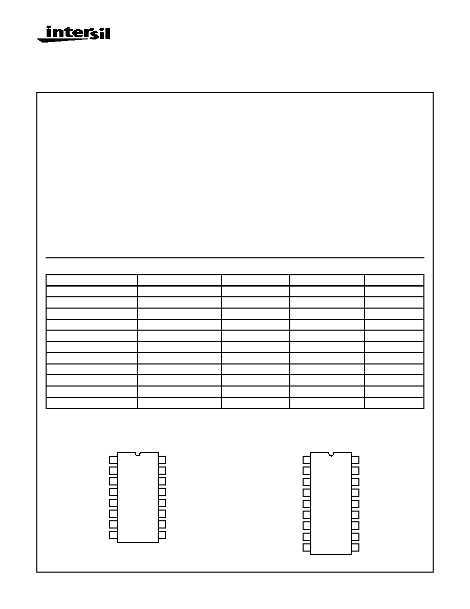
Ordering Information
Pinouts
PART NUMBER
LINEARITY (INL, DNL)
TEMP. RANGE (
o
C)
PACKAGE
PKG. NO.
AD7520JN, AD7530JN
0.2% (8-Bit)
0 to 70
16 Ld PDIP
E16.3
AD7520KN, AD7530KN
0.1% (9-Bit)
0 to 70
16 Ld PDIP
E16.3
AD7521JN, AD7531JN
0.2% (8-Bit)
0 to 70
18 Ld PDIP
E18.3
AD7521KN, AD7531KN
0.1% (9-Bit)
0 to 70
18 Ld PDIP
E18.3
AD7520LN, AD7530LN
0.05% (10-Bit)
-40 to 85
16 Ld PDIP
E16.3
AD7521LN, AD7531LN
0.05% (10-Bit)
-40 to 85
18 Ld PDIP
E18.3
AD7520JD
0.2% (8-Bit)
-25 to 85
16 Ld CERDIP
F16.3
AD7520KD
0.1% (9-Bit)
-25 to 85
16 Ld CERDIP
F16.3
AD7520LD
0.05% (10-Bit)
-25 to 85
16 Ld CERDIP
F16.3
AD7520SD, AD7520SD/883B
0.2% (8-Bit)
-55 to 125
16 Ld CERDIP
F16.3
AD7520UD, AD7520UD/883B
0.05% (10-Bit)
-55 to 125
16 Ld CERDIP
F16.3
AD7520, AD7530
(CERDIP, PDIP)
TOP VIEW
AD7521, AD7531
(PDIP)
TOP VIEW
14
15
16
9
13
12
11
10
1
2
3
4
5
7
6
8
I
OUT1
I
OUT2
GND
BIT 1 (MSB)
BIT 2
BIT 3
BIT 5
BIT 4
R
FEEDBACK
V+
BIT 10 (LSB)
BIT 9
BIT 8
BIT 7
BIT 6
V
REF
I
OUT1
I
OUT2
GND
BIT 1 (MSB)
BIT 2
BIT 3
BIT 5
BIT 4
R
FEEDBACK
V+
BIT 11
BIT 9
BIT 8
BIT 7
V
REF
10
11
12
13
14
15
16
17
18
9
8
7
6
5
4
3
2
1
BIT 12 (LSB)
BIT 10
BIT 6
August 1997
AD7520, AD7530,
AD7521, AD7531
10-Bit, 12-Bit, Multiplying D/A Converters
File Number
3104.1
CAUTION: These devices are sensitive to electrostatic discharge; follow proper IC Handling Procedures.
http://www.intersil.com or 407-727-9207
|
Copyright
©
Intersil Corporation 1999
10-8
Absolute Maximum Ratings
Thermal Information
Supply Voltage (V+ to GND). . . . . . . . . . . . . . . . . . . . . . . . . . . +17V
V
REF
. . . . . . . . . . . . . . . . . . . . . . . . . . . . . . . . . . . . . . . . . . . . .
±
25V
Digital Input Voltage Range . . . . . . . . . . . . . . . . . . . . . . . V+ to GND
Output Voltage Compliance . . . . . . . . . . . . . . . . . . . . -100mV to V+
Operating Conditions
Temperature Ranges
JN, KN, LN Versions . . . . . . . . . . . . . . . . . . . . . . . . . .0
o
C to 70
o
C
JD, KD, LD Versions . . . . . . . . . . . . . . . . . . . . . . . . -25
o
C to 85
o
C
SD, UD Versions . . . . . . . . . . . . . . . . . . . . . . . . . . -55
o
C to 125
o
C
Thermal Resistance (Typical, Note 1)
JA
(
o
C/W)
JC
(
o
C/W)
16 Ld PDIP Package . . . . . . . . . . . . . . . .
100
N/A
18 Ld PDIP Package . . . . . . . . . . . . . . . .
90
N/A
CERDIP Package . . . . . . . . . . . . . . . . . .
75
20
Maximum Junction Temperature (Hermetic Package) . . . . . . . . 175
o
C
Maximum Junction Temperature (Plastic Packages) . . . . . . . 150
o
C
Maximum Storage Temperature Range . . . . . . . . . .-65
o
C to 150
o
C
Maximum Lead Temperature (Soldering 10s) . . . . . . . . . . . . . 300
o
C
CAUTION: Stresses above those listed in "Absolute Maximum Ratings" may cause permanent damage to the device. This is a stress only rating and operation
of the device at these or any other conditions above those indicated in the operational sections of this specification is not implied.
The digital control inputs are zener protected; however, permanent damage may occur on unconnected units under high energy electrostatic fields. Keep
unused units in conductive foam at all times.
Do not apply voltages higher than V
DD
or less than GND potential on any terminal except V
REF
and R
FEEDBACK
.
NOTE:
1.
JA
is measured with the component mounted on an evaluation PC board in free air.
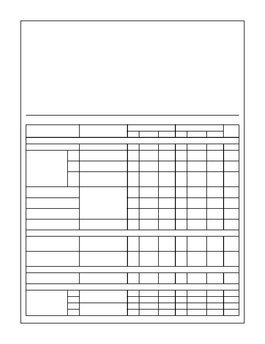
Electrical Specifications
V+ = +15V, V
REF
= +10V, T
A
= 25
o
C Unless Otherwise Specified
PARAMETER
TEST CONDITIONS
AD7520/AD7530
AD7521/AD7531
UNITS
MIN
TYP
MAX
MIN
TYP
MAX
SYSTEM PERFORMANCE (Note 2)
Resolution
10
10
10
12
12
12
Bits
Nonlinearity
J, S
S Over -55
o
C to 125
o
C
(Notes 2, 5) (Figure 3)
-
-
±
0.2
(8-Bit)
-
-
±
0.2
(8-Bit)
% of
FSR
K
T Over -55
o
C to 125
o
C
(Figure 2)
-
-
±
0.1
(9-Bit)
-
-
±
0.1
(9-Bit)
% of
FSR
L, U
-10V
V
REF
+10V
U Over -55
o
C to 125
o
C
(Figure 2)
-
-
±
0.05
(10-Bit)
-
-
±
0.05
(10-Bit)
% of
FSR
Nonlinearity Tempco
-10V
V
REF
+10V
(Notes 3, 4)
-
-
±
2
-
-
±
2
ppm of
FSR/
o
C
Gain Error
-
±
0.3
-
-
±
0.3
-
% of
FSR
Gain Error Tempco
-
-
±
10
-
-
±
10
ppm of
FSR/
o
C
Output Leakage Current
(Either Output)
Over the Specified
Temperature Range
-
-
±
200
(
±
300)
-
-
±
200
(
±
300)
nA
DYNAMIC CHARACTERISTICS
Output Current Settling Time
To 0.05% of FSR (All Digital
Inputs Low To High And High
To Low) (Note 4) (Figure 7)
-
1.0
-
-
1.0
-
µ
s
Feedthrough Error
V
REF
= 20V
P-P
, 10kHz
(50kHz) All Digital Inputs Low
(Note 4) (Figure 6)
-
-
10
-
-
10
mV
P-P
REFERENCE INPUT
Input Resistance
All Digital Inputs High
I
OUT1
at Ground
5
10
20
5
10
20
k
ANALOG OUTPUT
Output Capacitance
I
OUT1
All Digital Inputs High
(Note 4) (Figure 5)
-
200
-
-
200
-
pF
I
OUT2
-
75
-
-
75
-
pF
I
OUT1
All Digital Inputs Low
(Note 4) (Figure 5)
-
75
-
-
75
-
pF
I
OUT2
-
200
-
-
200
-
pF
AD7520, AD7530, AD7521, AD7531

10-9
Functional Diagram
NOTES:
Switches shown for Digital Inputs "High".
Resistor values are typical.
Output Noise
Both Outputs
(Note 4) (Figure 4)
-
Equivalent
to 10k
-
-
Equivalent
to 10k
-
Johnson
Noise
DIGITAL INPUTS
Low State Threshold, V
IL
Over the Specified
Temperature Range
V
IN
= 0V or +15V
-
-
0.8
-
-
0.8
V
High State Threshold, V
IH
2.4
-
-
2.4
-
-
V
Input Current, I
IL
, I
IH
-
-
±
1
-
-
±
1
µ
A
Input Coding
See Tables 1 and 2
Binary/Offset Binary
POWER SUPPLY CHARACTERISTICS
Power Supply Rejection
V+ = 14.5V to 15.5V
(Note 3) (Figure 3)
-
±
0.005
-
-
±
0.005
-
% FSR/
%
V+
Power Supply Voltage Range
+5 to +15
+5 to +15
V
I+
All Digital Inputs at 0V or V+
Excluding Ladder Network
-
±
1
-
-
±
1
-
µ
A
All Digital Inputs High or Low
Excluding Ladder Network
-
-
2
-
-
2
mA
Total Power Dissipation
Including the Ladder Network
-
20
-
-
20
-
mW
NOTES:
2. Full scale range (FSR) is 10V for Unipolar and
±
10V for Bipolar modes.
3. Using internal feedback resistor R
FEEDBACK
.
4. Guaranteed by design, or characterization and not production tested.
5. Accuracy not guaranteed unless outputs at GND potential.
6. Accuracy is tested and guaranteed at V+ = 15V only.
Electrical Specifications
V+ = +15V, V
REF
= +10V, T
A
= 25
o
C Unless Otherwise Specified (Continued)
PARAMETER
TEST CONDITIONS
AD7520/AD7530
AD7521/AD7531
UNITS
MIN
TYP
MAX
MIN
TYP
MAX
20k
GND
I
OUT2
I
OUT1
R
FEEDBACK
BIT 3
BIT 2
MSB
V
REF
20k
20k
20k
20k
20k
10k
10k
10k
10k
SPDT NMOS
SWITCHES
10k
AD7520, AD7530, AD7521, AD7531

10-10
Definition of Terms
Nonlinearity: Error contributed by deviation of the DAC
transfer function from a "best straight line" through the actual
plot of transfer function. Normally expressed as a percent-
age of full scale range or in (sub)multiples of 1 LSB.
Resolution: It is addressing the smallest distinct analog
output change that a D/A converter can produce. It is
commonly expressed as the number of converter bits. A
converter with resolution of n bits can resolve output changes
of 2
-N
of the full-scale range, e.g., 2
-N
V
REF
for a unipolar
conversion. Resolution by no means implies linearity.
Settling Time: Time required for the output of a DAC to set-
tle to within specified error band around its final value (e.g.,
1
/
2
LSB) for a given digital input change, i.e., all digital inputs
LOW to HIGH and HIGH to LOW.
Gain Error: The difference between actual and ideal analog
output values at full scale range, i.e., all digital inputs at
HIGH state. It is expressed as a percentage of full scale
range or in (sub)multiples of 1 LSB.
Feedthrough Error: Error caused by capacitive coupling
from V
REF
to I
OUT1
with all digital inputs LOW.
Output Capacitance: Capacitance from I
OUT1
and I
OUT2
terminals to ground.
Output Leakage Current: Current which appears on I
OUT1
terminal when all digital inputs are LOW or on I
OUT2
terminal when all digital inputs are HIGH.
Detailed Description
The AD7520, AD7530, AD7521 and AD7531 are monolithic,
multiplying D/A converters. A highly stable thin film R-2R
resistor ladder network and NMOS SPDT switches form the
basis of the converter circuit, CMOS level shifters permit low
power TTL/CMOS compatible operation. An external voltage
or current reference and an operational amplifier are all that
is required for most voltage output applications.
A simplified equivalent circuit of the DAC is shown in the
Functional Diagram. The NMOS SPDT switches steer the lad-
der leg currents between I
OUT1
and I
OUT2
buses which must
be held either at ground potential. This configuration main-
tains a constant current in each ladder leg independent of the
input code.
Converter errors are further reduced by using separate
metal interconnections between the major bits and the
outputs. Use of high threshold switches reduce offset (leak-
age) errors to a negligible level.
The level shifter circuits are comprised of three inverters with
positive feedback from the output of the second to the first, see
Figure 1. This configuration results in TTL/CMOS compatible
operation over the full military temperature range. With the lad-
der SPDT switches driven by the level shifter, each switch is
binarily weighted for an ON resistance proportional to the
respective ladder leg current. This assures a constant voltage
drop across each switch, creating equipotential terminations for
the 2R ladder resistors and highly accurate leg currents.
Pin Descriptions
AD7520/30
AD7521/31
PIN NAME
DESCRIPTION
1
1
I
OUT1
Current Out summing junction of the R2R ladder network.
2
2
I
OUT2
Current Out virtual ground, return path for the R2R ladder network.
3
3
GND
Digital Ground. Ground potential for digital side of D/A.
4
4
Bits 1(MSB)
Most Significant Digital Data Bit.
5
5
Bit 2
Digital Bit 2.
6
6
Bit 3
Digital Bit 3.
7
7
Bit 4
Digital Bit 4.
8
8
Bit 5
Digital Bit 5.
9
9
Bit 6
Digital Bit 6.
10
10
Bit 7
Digital Bit 7.
11
11
Bit 8
Digital Bit 8.
12
12
Bit 9
Digital Bit 9.
13
13
Bit 10
Digital Bit 10 (AD7521/31). Least Significant Digital Data Bit (AD7520/30).
-
14
Bit 11
Digital Bit 11 (AD7521/31).
-
15
Bit 12
Least Significant Digital Data Bit (AD7521/31).
14
16
V+
Power Supply +5V to +15V.
15
17
V
REF
Voltage Reference Input to set the output range. Supplies the R2R resistor ladder.
16
18
R
FEEDBACK
Feedback resistor used for the current to voltage conversion when using an external Op Amp.
V+
DTL/TTL/
CMOS INPUT
1 3
4
5
6
7
2
8
9
TO LADDER
I
OUT2
I
OUT1
FIGURE 1. CMOS SWITCH
AD7520, AD7530, AD7521, AD7531
10-11
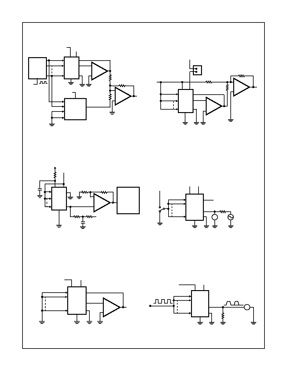
Test Circuits
The following test circuits apply for the AD7520. Similar circuits are used for the AD7530, AD7521 and AD7531.
FIGURE 2. NONLINEARITY
FIGURE 3. POWER SUPPLY REJECTION
FIGURE 4. NOISE
FIGURE 5. OUTPUT CAPACITANCE
FIGURE 6. FEEDTHROUGH ERROR
FIGURE 7. OUTPUT CURRENT SETTLING TIME
10-BIT
BINARY
COUNTER
GND
15
16
1
5
4
13 3 2
AD7520
BIT 1
(MSB)
BIT 10
(LSB)
LINEARITY
ERROR
X 100
R
FEEDBACK
I
OUT1
I
OUT2
HA2600
-
+
V
REF
BIT 1
(LSB)
BIT 10
BIT 11
BIT 12
10k
0.01%
1M
10k
0.01%
CLOCK
+15V
V
REF
HA2600
-
+
12-BIT
REFERENCE
DAC
15
16
1
5
4
13 3 2
AD7520
BIT 1
(MSB)
BIT 10
(LSB)
HA2600
-
+
HA2600
-
+
500k
UNGROUNDED
SINE WAVE
GENERATOR
400Hz 1V
P-P
5k
0.01%
5K 0.01%
R
FEEDBACK
+15V
+10V
V
REF
I
OUT1
I
OUT2
14
GND
15
2
5
4
13 3 1
AD7520
101ALN
-
+
0.1
µ
F
I
OUT1
I
OUT2
14
10k
V
OUT
100
15
µ
F
1K
+15V
50k
1k
50V
f = 1kHz
BW = 1Hz
QUAN
TECH
MODEL 134D
WAVE
ANALYZER
+11V (ADJUST FOR V
OUT
= 0V)
15
16
1
5
4
13 3
2
AD7520
BIT 1 (MSB)
BIT 10 (LSB)
14
+15V
NC
SCOPE
100mV
P-P
1MHz
NC
1k
+15V
15
16
1
5
4
13 3
2
AD7520
BIT 1 (MSB)
BIT 10 (LSB)
14
+15V
V
REF
= 20V
P-P
GND
I
OUT1
I
OUT2
2
3
6
V
OUT
100kHz SINE WAVE
HA2600
-
+
15
1
5
4
13 3
2
AD7520
BIT 1 (MSB)
BIT 10 (LSB)
14
+15V
SCOPE
+100mV
100
GND
V
REF
DIGITAL
I
OUT2
EXTRAPOLATE
5t: 1% SETTLING (1mV)
8t: 0.03% SETTLING
t = RISE TIME
INPUT
+5V
0V
-10V
AD7520, AD7530, AD7521, AD7531