 | –≠–ª–µ–∫—Ç—Ä–æ–Ω–Ω—ã–π –∫–æ–º–ø–æ–Ω–µ–Ω—Ç: AD7541 | –°–∫–∞—á–∞—Ç—å:  PDF PDF  ZIP ZIP |

10-9
August 1997
AD7541
12-Bit, Multiplying D/A Converter
File Number
3107.1
Features
∑ 12-Bit Linearity 0.01%
∑ Pretrimmed Gain
∑ Low Gain and Linearity Tempcos
∑ Full Temperature Range Operation
∑ Full Input Static Protection
∑ TTL/CMOS Compatible
∑ +5V to +15V Supply Range
∑ 20mW Low Power Dissipation
∑ Current Settling Time 1
µ
s to 0.01% of FSR
∑ Four Quadrant Multiplication
Description
The AD7541 is a monolithic, low cost, high performance,
12-bit accurate, multiplying digital-to-analog converter
(DAC).
Intersil' wafer level laser-trimmed thin-film resistors on
CMOS circuitry provide true 12-bit linearity with TTL/CMOS
compatible operation.
Special tabbed-resistor geometries (improving time stability),
full input protection from damage due to static discharge by
diode clamps to V+ and ground, large I
OUT1
and I
OUT2
bus
lines (improving superposition errors) are some of the fea-
tures offered by Intersil AD7541.
Pin compatible with AD7521, this DAC provides accurate
four quadrant multiplication over the full military temperature
range.
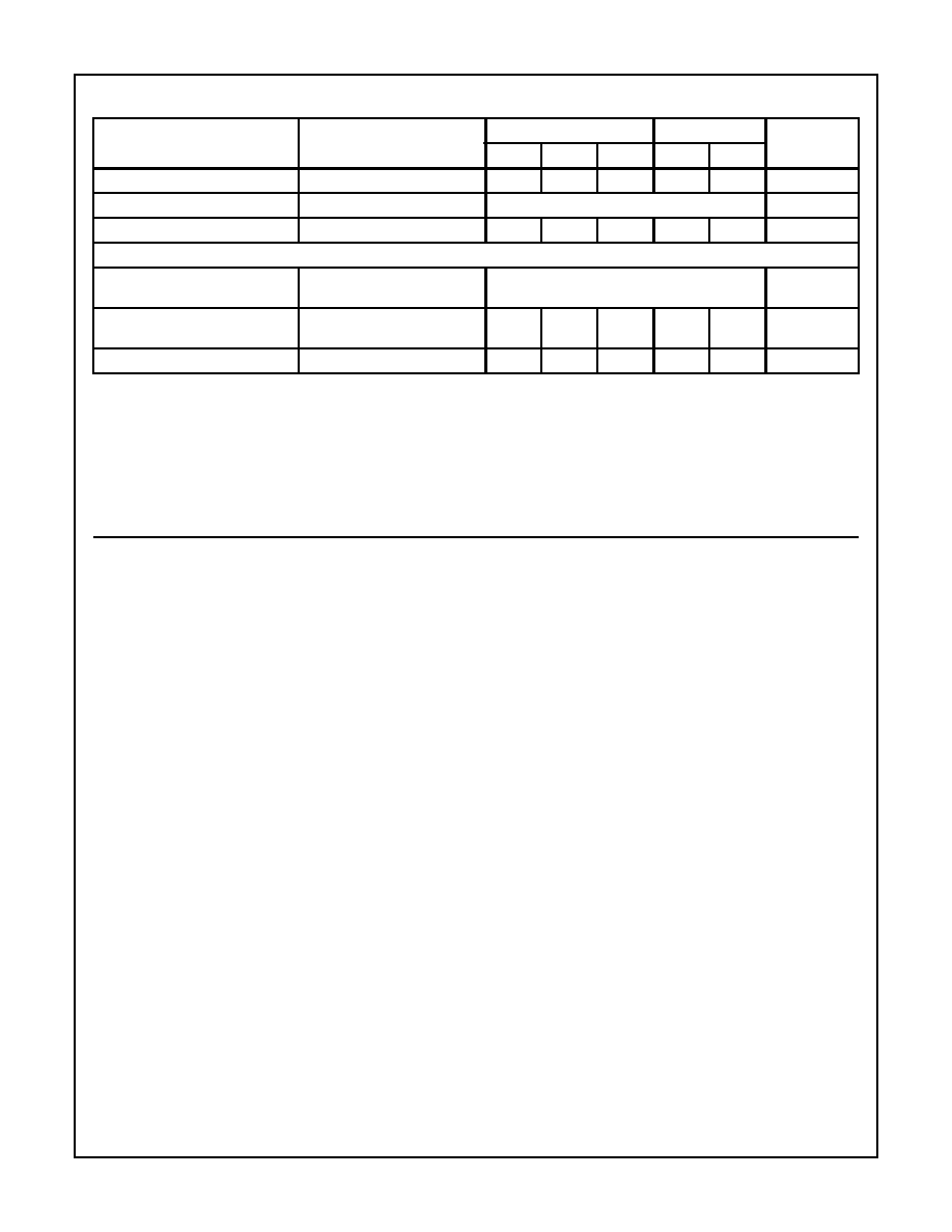
Ordering Information
PART NUMBER
NONLINEARITY
TEMP. RANGE (
o
C)
PACKAGE
PKG. NO.
AD7541JN
0.02% (11-Bit)
0 to 70
18 Ld PDIP
E18.3
AD7541KN
0.01% (12-Bit)
0 to 70
18 Ld PDIP
E18.3
AD7541LN
0.01% (12-Bit) Guaranteed
Monotonic
0 to 70
18 Ld PDIP
E18.3
Pinout
AD7541
(PDIP)
TOP VIEW
Functional Block Diagram
NOTE: Switches shown for digital inputs "High".
10
11
12
13
14
15
16
17
18
9
8
7
6
5
4
3
2
1
R
FEEDBACK
V+
BIT 12 (LSB)
BIT 11
BIT 10
BIT 9
BIT 8
V
REF IN
BIT 7
I
OUT1
I
OUT2
GND
BIT 1 (MSB)
BIT 2
BIT 3
BIT 5
BIT 4
BIT 6
MSB
(4)
20k
(3)
BIT 3
BIT 2
V
REF IN
20k
20k
20k
20k
20k
10k
10k
10k
10k
SPDT
NMOS
10k
I
OUT2
(2)
I
OUT1
(1)
R
FEEDBACK
(17)
SWITCHES
(18)
(5)
(6)
CAUTION: These devices are sensitive to electrostatic discharge; follow proper IC Handling Procedures.
http://www.intersil.com or 407-727-9207
|
Copyright
©
Intersil Corporation 1999

10-10
Absolute Maximum Ratings
Thermal Information
Supply Voltage (V+ to GND). . . . . . . . . . . . . . . . . . . . . . . . . . . +17V
V
REF
. . . . . . . . . . . . . . . . . . . . . . . . . . . . . . . . . . . . . . . . . . . . .
±
25V
Digital Input Voltage Range . . . . . . . . . . . . . . . . . . . . . . . V+ to GND
Output Voltage Compliance . . . . . . . . . . . . . . . . . . . . -100mV to V+
Operating Conditions
Temperature Range
JN, KN, LN Versions . . . . . . . . . . . . . . . . . . . . . . . . . .0
o
C to 70
o
C
Thermal Resistance (Typical, Note 1)
JA
(
o
C/W)
PDIP Package . . . . . . . . . . . . . . . . . . . . . . . . . . . . .
90
Maximum Junction Temperature . . . . . . . . . . . . . . . . . . . . . . . 150
o
C
Maximum Storage Temperature . . . . . . . . . . . . . . . .-65
o
C to 150
o
C
Maximum Lead Temperature (Soldering 10s) . . . . . . . . . . . . . 300
o
C
CAUTION: Stresses above those listed in "Absolute Maximum Ratings" may cause permanent damage to the device. This is a stress only rating and operation
of the device at these or any other conditions above those indicated in the operational sections of this specification is not implied.
NOTE:
1.
JA
is measured with the component mounted on an evaluation PC board in free air.
Electrical Specifications
V+ = +15V, V
REF
= +10V, V
OUT1
= V
OUT2
= 0V, T
A
= 25
o
C, Unless Otherwise Specified
PARAMETER
TEST CONDITIONS
T
A
= 25
o
C
T
A
MIN-MAX
UNITS
MIN
TYP
MAX
MIN
MAX
SYSTEM PERFORMANCE
Resolution
12
-
-
12
-
Bits
Nonlinearity
A, S, J
-10V
V
REF
+10V
V
OUT1
= V
OUT2
= 0V
See Figure 3
(Note 5)
-
-
±
0.024
-
±
0.024
% of FSR
B, T, K
-
-
±
0.012
-
±
0.012
% of FSR
L
-
-
±
0.012
-
±
0.012
% of FSR
Monotonicity
Guaranteed
Gain Error
-10V
V
REF
+10V (Note 5)
-
-
±
0.3
-
±
0.4
% of FSR
Output Leakage Current
(Either Output)
V
OUT1
= V
OUT2
= 0
-
-
±
50
-
±
200
nA
DYNAMIC CHARACTERISTICS
Power Supply Rejection
V+ = 14.5V to 15.5V
See Figure 5 (Note 5)
-
-
±
0.005
-
±
0.01
% of FSR/% of
V+
Output Current Settling Time
To 0.1% of FSR
See Figure 9 (Note 6)
-
-
1
-
1
µ
s
Feedthrough Error
V
REF
= 20V
P-P
, 10kHz
All Digital Inputs Low
See Figure 8 (Note 6)
-
-
1
-
1
mV
P-P
REFERENCE INPUTS
Input Resistance
All Digital Inputs High
I
OUT1
at Ground
5
10
20
5
20
k
ANALOG OUTPUT
Voltage Compliance
Both Outputs, See Maximum
Ratings (Note 7)
-100mV to V+
Output Capacitance
C
OUT1
All Digital Inputs High
See Figure 7 (Note 6)
-
-
200
-
200
pF
C
OUT2
-
-
60
-
60
pF
C
OUT1
All Digital Inputs Low)
See Figure 7 (Note 6)
-
-
60
-
60
pF
C
OUT2
-
-
200
-
200
pF
Output Noise (Both Outputs)
See Figure 6
Equivalent to 10k
Johnson Noise
DIGITAL INPUTS
Low State Threshold, V
IL
(Notes 2, 6)
-
-
0.8
-
0.8
V
High State Threshold, V
IH
2.4
-
-
2.4
-
V
AD7541
10-11
Definition of Terms
Nonlinearity: Error contributed by deviation of the DAC
transfer function from a "best fit straight line" function. Nor-
mally expressed as a percentage of full scale range. For a
multiplying DAC, this should hold true over the entire V
REF
range.
Resolution: Value of the LSB. For example, a unipolar
converter with n bits has a resolution of LSB = (V
REF
)/2
-N
. A
bipolar converter of n bits has a resolution of
LSB = (V
REF
)/2
-(N-1)
. Resolution in no way implies linearity.
Settling Time: Time required for the output function of the
DAC to settle to within
1
/
2
LSB for a given digital input
stimulus, i.e., 0 to Full Scale.
Gain Error: Ratio of the DAC's operational amplifier output
voltage to the nominal input voltage value.
Feedthrough Error: Error caused by capacitive coupling
from V
REF
to output with all switches OFF.
Output Capacitance: Capacitance from I
OUT1
, and I
OUT2
terminals to ground.
Output Leakage Current: Current which appears on
I
OUT1
, terminal when all digital inputs are LOW or on I
OUT2
terminal when all inputs are HIGH.
Detailed Description
The AD7541 is a 12-bit, monolithic, multiplying D/A converter.
A highly stable thin film R-2R resistor ladder network and
NMOS SPDT switches form the basis of the converter circuit.
CMOS level shifters provide low power TTL/CMOS compati-
ble operation. An external voltage or current reference and an
operational amplifier are all that is required for most voltage
output applications. A simplified equivalent circuit of the DAC
is shown on page 1, (Functional Diagram). The NMOS SPDT
switches steer the ladder leg currents between I
OUT1
and
I
OUT2
buses which must be held at ground potential. This
configuration maintains a constant current in each ladder leg
independent of the input code. Converter errors are further
eliminated by using wider metal interconnections between the
major bits and the outputs. Use of high threshold switches
reduces the offset (leakage) errors to a negligible level.
Each circuit is laser-trimmed, at the wafer level, to better than
12-bits linearity. For the first four bits of the ladder, special
trim-tabbed geometries are used to keep the body of the
resistors, carrying the majority of the output current, undis-
turbed. The resultant time stability of the trimmed circuits is
comparable to that of untrimmed units.
The level shifter circuits are comprised of three inverters with
a positive feedback from the output of the second to first
(Figure 1). This configuration results in TTL/COMS compati-
ble operation over the full military temperature range. With
the ladder SPDT switches driven by the level shifter, each
switch is binary weighted for an "ON" resistance proportional
to the respective ladder leg current. This assures a constant
voltage drop across each switch, creating equipotential ter-
minations for the 2R ladder resistor, resulting in accurate leg
currents.
Input Current
V
IN
= 0V or V+ (Note 6)
-
-
±
1
-
±
1
µ
A
Input Coding
See Tables 1 and 2 (Note 6)
Binary/Offset Binary
Input Capacitance
(Note 6)
-
-
8
-
8
pF
POWER SUPPLY CHARACTERISTICS
Power Supply Voltage Range
Accuracy Is Not Guaranteed
Over This Range
+5 to +16
V
I+
All Digital Inputs High or Low
(Excluding Ladder Network)
-
-
2.0
-
2.5
mA
Total Power Dissipation
(Including Ladder Network)
-
20
-
-
-
mW
NOTES:
2. The digital control inputs are zener protected; however, permanent damage may occur on unconnected units under high energy
electrostatic fields. Keep unused units in conductive foam at all times.
3. Do not apply voltages higher than V
DD
or less than GND potential on any terminal except V
REF
and R
FEEDBACK
.
4. Full scale range (FSR) is 10V for unipolar and
±
10V for bipolar modes.
5. Using internal feedback resistor, R
FEEDBACK
.
6. Guaranteed by design or characterization and not production tested.
7. Accuracy not guaranteed unless outputs at ground potential.
Electrical Specifications
V+ = +15V, V
REF
= +10V, V
OUT1
= V
OUT2
= 0V, T
A
= 25
o
C, Unless Otherwise Specified (Continued)
PARAMETER
TEST CONDITIONS
T
A
= 25
o
C
T
A
MIN-MAX
UNITS
MIN
TYP
MAX
MIN
MAX
AD7541
10-12
Typical Applications
General Recommendations
Static performance of the AD7541 depends on I
OUT1
and
I
OUT2
(pin 1 and pin 2) potentials being exactly equal to
GND (pin 3).
The output amplifier should be selected to have a low input
bias current (typically less than 75nA), and a low drift
(depending on the temperature range). The voltage offset of
the amplifier should be nulled (typically less than
±
200
µ
V).
The bias current compensation resistor in the amplifier's
non-inverting input can cause a variable offset. Non-inverting
input should be connected to GND with a low resistance
wire.
Ground-loops must be avoided by taking all pins going to
GND to a common point, using separate connections.
The V+ (pin 18) power supply should have a low noise level
and should not have any transients exceeding +17V.
Unused digital inputs must be connected to GND or V
DD
for
proper operation.
A high value resistor (~1M
) can be used to prevent static
charge accumulation, when the inputs are open-circuited for
any reason.
When gain adjustment is required, low tempco
(approximately 50ppm/
o
C) resistors or trim-pots should be
selected.
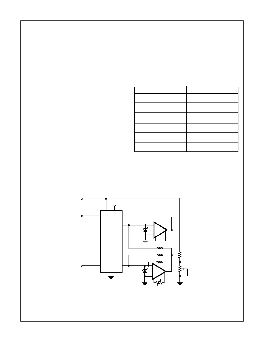
Unipolar Binary Operation
The circuit configuration for operating the AD7541 in
unipolar mode is shown in Figure 2. With positive and
negative V
REF
values the circuit is capable of 2-Quadrant
multiplication. The "Digital Input Code/Analog Output Value"
table for unipolar mode is given in Table 1. A Schottky diode
(HP5082-2811 or equivalent) prevents I
OUT1
from negative
excursions which could damage the device. This precaution
is only necessary with certain high speed amplifiers.
Zero Offset Adjustment
1. Connect all digital inputs to GND.
2. Adjust the offset zero adjust trimpot of the output
operational amplifier for 0V
±
0.5mV (Max) at V
OUT
.
Gain Adjustment
1. Connect all digital inputs to V
DD
.
2. Monitor V
OUT
for a -V
REF
(1
1
/
2
12
) reading.
3. To increase V
OUT
, connect a series resistor, (0
to
250
), in the I
OUT1
amplifier feedback loop.
4. To decrease V
OUT
, connect a series resistor, (0
to 250
),
between the reference voltage and the V
REF
terminal.
Bipolar (Offset Binary) Operation
The circuit configuration for operating the AD7541 in the
bipolar mode is given in Figure 3. Using offset binary digital
input codes and positive and negative reference voltage
values Four-Quadrant multiplication can be realized. The
"Digital Input Code/Analog Output Value" table for bipolar
mode is given in Table 2.
V+
TTL/CMOS
INPUT
1 3
4
5
6
7
2
8
9
TO LADDER
I
OUT2
I
OUT1
FIGURE 1. CMOS SWITCH
TABLE 1. CODE TABLE - UNIPOLAR BINARY OPERATION
DIGITAL INPUT
ANALOG OUTPUT
111111111111
-V
REF
(1 -
1
/
2
12
)
100000000001
-V
REF
(
1
/
2
+
1
/
2
12
)
100000000000
-V
REF
/2
011111111111
-V
REF
(
1
/
2
-
1
/
2
12
)
000000000001
-V
REF
(
1
/
2
12
)
000000000000
0
17
18
1
4
15
3
2
AD7541
BIT 1 (MSB)
BIT 12 (LSB)
16
+15V
V
REF
GND
I
OUT1
I
OUT2
6
V
OUT
-
+
R
FEEDBACK
DIGITAL
INPUT
CR1
5
±
10V
A
FIGURE 2. UNIPOLAR BINARY OPERATION (2-QUADRANT
MULTIPLICATION)
AD7541
10-13
A "Logic 1" input at any digital input forces the corresponding
ladder switch to steer the bit current to I
OUT1
bus. A "Logic
0" input forces the bit current to I
OUT2
bus. For any code the
I
OUT1
and I
OUT2
bus currents are complements of one
another. The current amplifier at I
OUT2
changes the polarity
of I
OUT2
current and the transconductance amplifier at
I
OUT1
output sums the two currents. This configuration dou-
bles the output range of the DAC. The difference current
resulting at zero offset binary code, (MSB = "Logic 1", All
other bits = "Logic 0"), is corrected by using an external
resistive divider, from V
REF
to I
OUT2
.
Offset Adjustment
1. Adjust V
REF
to approximately +10V.
2. Set R4 to zero.
3. Connect all digital inputs to "Logic 1".
4. Adjust I
OUT1
amplifier offset zero adjust trimpot for 0V
±
0.1mV at I
OUT2
amplifier output.
5. Connect a short circuit across R2.
6. Connect all digital inputs to "Logic 0".
7. Adjust I
OUT2
amplifier offset zero adjust trimpot for 0V
±
0.1mV at I
OUT1
amplifier output.
8. Remove short circuit across R2.
9. Connect MSB (Bit 1) to "Logic 1" and all other bits to "Logic 0".
10. Adjust R4 for 0V
±
0.2mV at V
OUT
.
Gain Adjustment
1. Connect all digital inputs to V
DD
.
2. Monitor V
OUT
for a -V
REF
(1 -
1
/
2
11
) volts reading.
3. To increase V
OUT
, connect a series resistor, (0
to
250
), in the I
OUT1
amplifier feedback loop.
4. To decrease V
OUT
, connect a series resistor, (0
to 250
),
between the reference voltage and the V
REF
terminal.
TABLE 2. CODE TABLE - BIPOLAR (OFFSET BINARY)
OPERATION
DIGITAL INPUT
ANALOG OUTPUT
111111111111
-V
REF
(1 -
1
/
2
11
)
100000000001
-V
REF
(
1
/
2
11
)
100000000000
0
011111111111
V
REF
(
1
/
2
11
)
000000000001
V
REF
(1 -
1
/
2
11
)
000000000000
V
REF
I
OUT2
6
6
I
OUT1
17
18
1
4
15
3
2
AD7541
BIT 1 (MSB)
BIT 12 (LSB)
16
+15V
V
REF
DIGITAL
INPUT
±
10V
R1 10K
R5 10K
V
OUT
-
+
A1
-
+
A2
GND
R2 10K
R3
390K
R4
500
NOTE: R1 and R2 should be 0.01%, low-TCR resistors.
FIGURE 3. BIPOLAR OPERATION (4-QUADRANT MULTIPLICATION)
AD7541