 | –≠–ª–µ–∫—Ç—Ä–æ–Ω–Ω—ã–π –∫–æ–º–ø–æ–Ω–µ–Ω—Ç: AD7545 | –°–∫–∞—á–∞—Ç—å:  PDF PDF  ZIP ZIP |
10-10
August 1997
AD7545
12-Bit, Buffered, Multiplying CMOS DAC
Features
∑ 12-Bit Resolution
∑ Low Gain T.C. 2ppm/
o
C (Typ)
∑ Fast TTL/CMOS Compatible Data Latches
∑ Single +5V to +15V Supply
∑ Low Power
∑ Low Cost
∑ /883 Processed Versions Available
Description
The AD7545 is a low cost monolithic 12-bit, CMOS
multiplying DAC with on-board data latches. Data is loaded
in a single 12-bit wide word which allows interfacing directly
to most 12-bit and 16-bit bus systems. Loading of the input
latches is under the control of the CS and WR inputs. A logic
low on these control inputs makes the input latches transpar-
ent allowing direct unbuffered operation of the DAC.
Ordering Information
PART NUMBER
TEMP.
RANGE (
o
C)
PACKAGE
PKG.
NO.
AD7545JN
0 to 70
20 Ld PDIP
E20.3
AD7545KN
0 to 70
20 Ld PDIP
E20.3
AD7545AN
-40 to 85
20 Ld PDIP
E20.3
AD7545BN
-40 to 85
20 Ld PDIP
E20.3
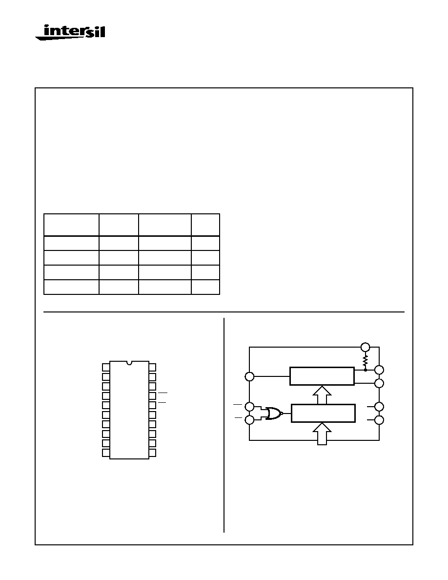
Pinout
AD7545
(PDIP)
TOP VIEW
Functional Diagram
11
12
13
14
15
16
17
18
20
19
10
9
8
7
6
5
4
3
2
1
OUT 1
AGND
DGND
DB11 (MSB)
DB10
DB9
DB7
DB8
DB6
DB5
R
FB
V
DD
WR
CS
V
REF
DB0 (LSB)
DB1
DB2
DB3
DB4
12-BIT
MULTIPLYING DAC
DB11 - DB0
(PINS 4 - 15)
12
12
INPUT DATA LATCHES
19
17
16
2
1
3
18
20
R
FB
R
OUT1
AGND
V
DD
DGND
V
REF
WR
CS
AD7545
File Number
3108.1
CAUTION: These devices are sensitive to electrostatic discharge; follow proper IC Handling Procedures.
http://www.intersil.com or 407-727-9207
|
Copyright
©
Intersil Corporation 1999

10-11
Absolute Maximum Ratings
Thermal Information
Supply Voltage (V
DD
to DGND) . . . . . . . . . . . . . . . . . . . -0.3V, +17V
Digital Input Voltage to DGND . . . . . . . . . . . . . . . .-0.3V, V
DD
+0.3V
V
RFB
, V
REF
to DGND . . . . . . . . . . . . . . . . . . . . . . . . . . . . . . .
±
25V
V
PIN1
to DGND . . . . . . . . . . . . . . . . . . . . . . . . . . .-0.3V, V
DD
+0.3V
AGND to DGND . . . . . . . . . . . . . . . . . . . . . . . . . . .-0.3V, V
DD
+0.3V
Operating Conditions
Temperature Ranges
Commercial (J, K, Grades) . . . . . . . . . . . . . . . . . . . . .0
o
C to 70
o
C
Industrial (A, B, Grades) . . . . . . . . . . . . . . . . . . . . . -40
o
C to 85
o
C
Extended (S Grades) . . . . . . . . . . . . . . . . . . . . . . -55
o
C to 125
o
C
Thermal Resistance (Typical, Note 1)
JA
(
o
C/W)
PDIP Package . . . . . . . . . . . . . . . . . . . . . . . . . . . . .
125
Maximum Junction Temperature (PDIP Package) . . . . . . . . . 150
o
C
Maximum Storage Temperature Range . . . . . . . . . .-65
o
C to 150
o
C
Maximum Lead Temperature (Soldering 10s) . . . . . . . . . . . . 300
o
C
CAUTION: Stresses above those listed in "Absolute Maximum Ratings" may cause permanent damage to the device. This is a stress only rating and operation
of the device at these or any other conditions above those indicated in the operational sections of this specification is not implied.
NOTE:
1.
JA
is measured with the component mounted on an evaluation PC board in free air.
Electrical Specifications
T
A
= See Note 2, V
REF
= +10V, V
OUT1
= 0V, AGND = DGND, Unless Otherwise Specified
PARAMETER
TEST CONDITIONS
V
DD
= +5V
V
DD
= +15V
UNITS
MIN
TYP
MAX
MIN
TYP
MAX
STATIC PERFORMANCE
Resolution
12
12
Bits
Relative Accuracy
J, A, S
-
-
±
2
-
-
±
2
LSB
K, B
-
-
±
1
-
-
±
1
LSB
Differential Nonlinearity
J, A, S 10-Bit Monotonic T
MIN
to T
MAX
-
-
±
4
-
-
±
4
LSB
K, B
12-Bit Monotonic T
MIN
to T
MAX
-
-
±
1
-
-
±
1
LSB
Gain Error
(Using Internal RFB)
J, A, S DAC Register Loaded with
1111 1111 1111
-
-
±
20
-
-
±
25
LSB
K, B
Gain Error is Adjustable
Using the Circuits of
Figures 4 and 5 (Note 3)
-
-
±
10
-
-
±
15
LSB
Gain Temperature Coefficient
Gain/
Temperature
Typical Value is 2ppm/
o
C for
V
DD
= +5V (Note 4)
-
-
±
5
-
-
±
10
ppm/
o
C
DC Supply Rejection
Gain/
V
DD
V
DD
=
±
5%
0.015
-
0.03
0.01
-
0.02
%
Output Leakage Current
at OUT1
J, K
DB0 - DB11 = 0V; WR,
CS = 0V (Note 2)
-
-
50
-
-
50
nA
A, B
-
-
50
-
-
50
nA
S
-
-
200
-
-
200
nA
DYNAMIC CHARACTERISTICS
Current Setting Time
To
1
/
2
LSB, OUT1 LOAD = 100
,
DAC Output Measured from
Falling Edge of WR, CS = 0V
(Note 4)
-
-
2
-
-
2
µ
s
Propagation Delay from Digital Input
Change to 90% of Final Analog
Output
OUT1 LOAD = 100
,
C
EXT
= 13pF (Notes 4 and 5)
-
-
300
-
-
250
ns
Digital to Analog Glitch Impulse
V
REF
= AGND
-
400
-
-
250
-
nV/s
AC Feedthrough at OUT1
V
REF
=
±
10V, 10kHz Sinewave
(Note 6)
-
5
-
-
5
-
mV
P-P
ANALOG OUTPUTS
Output Capacitance
C
OUT1
DB0 - DB11 = 0V,
WR, CS = 0V (Note 4)
-
-
70
-
-
70
pF
C
OUT1
DB0 - DB11 = V
DD
,
WR, CS = 0V (Note 4)
-
-
200
-
-
200
pF
AD7545
10-12
REFERENCE INPUT
Input Resistance (Pin 19 to GND)
Input Resistance
TC = -300ppm/
o
C (Typ)
7
-
-
7
-
-
k
Typical Input Resistance = 11k
-
-
25
-
-
25
k
DIGITAL INPUTS
Input High Voltage, V
IH
2.4
-
-
-
-
13.5
V
Input Low Voltage, V
IL
-
-
0.8
-
-
1.5
V
Input Current, I
IN
V
IN
= 0 or V
DD
(Note 7)
±
1
-
±
10
±
1
-
±
10
µ
A (Max)
Input Capacitance
DB0 - DB11
V
IN
= 0 (Note 4)
-
-
7
-
-
7
pF
WR, CS
V
IN
= 0 (Note 4)
-
-
20
-
-
20
pF
SWITCHING CHARACTERISTICS (Note 4)
Chip Select to Write Setup Time, t
CS
See Figure 1
380
200
-
200
120
-
ns
Chip Select to Write Hold Time, t
CH
See Figure 1
0
-
-
0
-
-
ns
Write Pulse Width, t
WR
t
CS
t
WR
, t
CH
0, See Figure 1
400
175
-
240
100
ns
Data Setup Time, t
DS
See Figure 1
210
100
-
120
60
-
ns
Data Hold Time, t
DH
See Figure 1
10
-
-
10
-
-
ns
POWER SUPPLY CHARACTERISTICS
I
DD
All Digital Inputs V
IL
or V
IH
-
-
2
-
-
2
mA
All Digital Inputs 0V or V
DD
-
100
500
-
100
500
µ
A
All Digital Inputs 0V or V
DD
-
10
-
-
10
-
µ
A
NOTES:
2. Temperature Ranges as follows: J, K versions:
0
o
C to 70
o
C
A, B versions: -20
o
C to 85
o
C
S version:
-55
o
C to 125
o
C
T
A
= 25
o
C for TYP Specifications. MIN and MAX are measured over the specified operating range.
3. This includes the effect of 5ppm maximum gain TC.
4. Parameter not tested. Parameter guaranteed by design, simulation, or characterization.
5. DB0 - DB11 = 0V to V
DD
or V
DD
to 0V in plastic and sidebraze package.
6. Feedthrough can be further reduced by connecting the metal lid on the ceramic package to DGND.
7. Logic inputs are MOS gates. Typical input current (25
o
C) is less than 1nA.
8. Typical values are not guaranteed but reflect mean performance specification.
Specifications subject to change without notice.
Electrical Specifications
T
A
= See Note 2, V
REF
= +10V, V
OUT1
= 0V, AGND = DGND, Unless Otherwise Specified (Continued)
PARAMETER
TEST CONDITIONS
V
DD
= +5V
V
DD
= +15V
UNITS
MIN
TYP
MAX
MIN
TYP
MAX
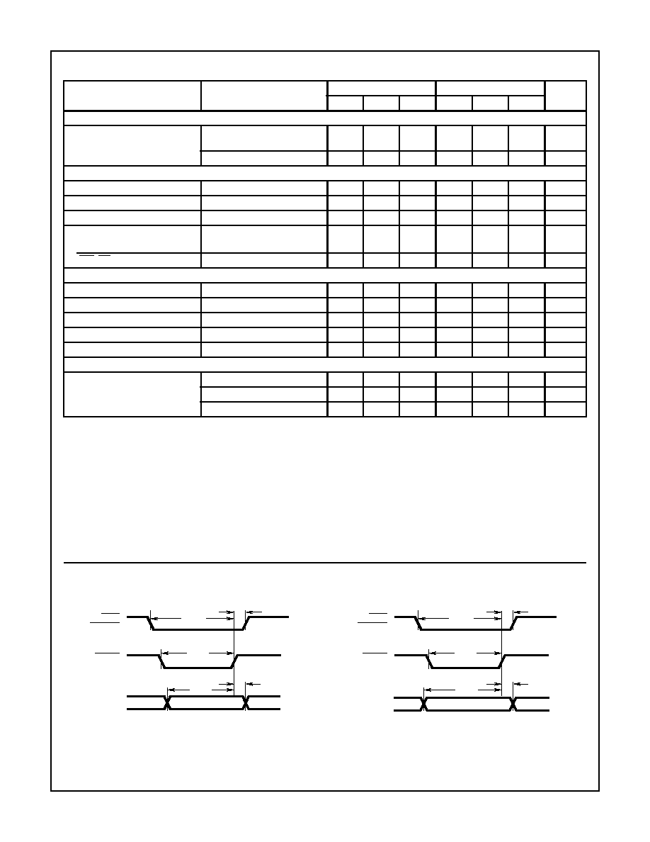
Timing Diagrams
FIGURE 1A. TYPICAL WRITE CYCLE
FIGURE 1B. PREFERRED WRITE CYCLE
FIGURE 1. WRITE CYCLE TIMING DIAGRAM
DATA VALID
CHIP
SELECT
WRITE
DATA IN
(DB0 - DB11)
V
DD
0
V
DD
V
DD
0
0
t
CS
t
WR
t
DS
t
DH
t
CH
DATA VALID
CHIP
SELECT
WRITE
DATA IN
(DB0 - DB11)
V
DD
0
V
DD
V
DD
0
0
t
CS
t
WR
t
DS
t
DH
t
CH
AD7545
10-13
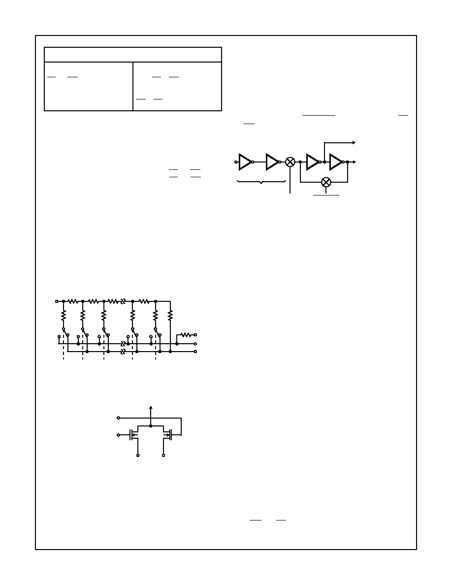
Circuit Information - D/A Converter Section
Figure 2 shows a simplified circuit of the D/A converter
section of the AD7545. Note that the ladder termination
resistor is connected to AGND. R is typically 11k
.
The binary weighted currents are switched between the OUT1
bus line and AGND by N-Channel switches, thus maintaining a
constant current in each ladder leg independent of the switch
state. One of the current switches is shown in Figure 3.
The capacitance at the OUT1 bus line, C
OUT1
, is code
dependent and varies from 70pF (all switches to AGND) to
200pF (all switches to OUT1).
The input resistance at V
REF
(Figure 2) is always equal to
R
LDR
(R
LDR
is the R/2R ladder characteristic resistance and is
equal to the value "R"). Since R
IN
at the V
REF
pin is constant,
the reference terminal can be driven by a reference voltage or a
reference current, AC or DC, of positive or negative polarity. (If a
current source is used, a low temperature coefficient external
R
FB
is recommended to define scale factor).
Circuit Information - Digital Section
Figure 4 shows the digital structure for one bit. The digital
signals CONTROL and CONTROL are generated from CS
and WR.
The input buffers are simple CMOS inverters designed such
that when the AD7545 is operated with V
DD
= 5V, the buffers
convert TTL input levels (2.4V and 0.8V) into CMOS logic
levels. When V
IN
is in the region of 2.0V to 3.5V the input
buffers operate in their linear region and draw current from
the power supply. To minimize power supply currents it is
recommended that the digital input voltages be as close to
the supply rails (V
DD
and DGND) as is practically possible.
The AD7545 may be operated with any supply voltage in the
range 5V
V
DD
15V. With V
DD
= +15V the input logic
levels are CMOS compatible only, i.e., 1.5V and 13.5V.
Application
Output Offset
CMOS current-steering D/A converters exhibit a code
dependent output resistance which in turn causes a code
dependent amplifier noise gain. The effect is a code depen-
dent differential nonlinearity term at the amplifier output
which depends on V
OS
where V
OS
is the amplifier input
offset voltage. To maintain monotonic operation it is recom-
mended that V
OS
be no greater than (25 x 10
-6
) (V
REF
) over
the temperature range of operation.
General Ground Management
AC or transient voltages between AGND and DGND can
cause noise injection into the analog output. The simplest
method of ensuring that voltages at AGND and DGND are
equal is to tie AGND and DGND together at the AD7545. In
more complex systems where the AGND and DGND con-
nection is on the backplane, it is recommended that two
diodes be connected in inverse parallel between the AD7545
AGND and DGND pins (1N914 or equivalent).
Digital Glitches
When WR and CS are both low the latched are transparent
and the D/A converter inputs follow the data inputs. In some
MODE SELECTION
WRITE MODE:
CS and WR low, DAC responds
to data bus (DB0 - DB11) inputs
HOLD MODE:
Either CS or WR high, data bus
(DB0 - DB11) is locked out; DAC
holds last data present when
WR or CS assumed high state.
NOTES:
9. V
DD
= +5V; t
r
= t
f
= 20ns
10. V
DD
= +15V; t
r
= t
f
= 40ns
11. All input signal rise and fall times measured from 10% to 90% of
V
DD
.
12. Timing measurement reference level is (V
IH
+ V
IL
)/2.
13. Since input data latches are transparent for CS and WR both
low, it is preferred to have data valid before CS and WR both go
low. This prevents undesirable changes at the analog output
while the data inputs settle.
DB11
(MSB)
V
REF
R
R
R
R
2R
2R
2R
2R
2R
2R
R
FB
OUT1
AGND
DB10
DB9
DB1
DB0
(LSB)
FIGURE 2. SIMPLIFIED D/A CIRCUIT OF AD7545
TO LADDER
FROM
INTERFACE
LOGIC
AGND
OUT1
FIGURE 3. N-CHANNEL CURRENT STEERING SWITCH
FIGURE 4. DIGITAL INPUT STRUCTURE
CONTROL
CONTROL
INPUTS
BUFFERS
TO OUT1 SWITCH
TO AGND SWITCH
AD7545
10-14
bus systems, data on the data bus is not always valid for the
whole period during which WR is low and as a result invalid
data can briefly occur at the D/A converter inputs during a
write cycle. Such invalid data can cause unwanted glitches
at the output of the D/A converter. The solution to this prob-
lem, if it occurs, is to retime the write pulse (WR) so that it
only occurs when data is valid.
Another cause of digital glitches is capacitive coupling from
the digital lines to the OUT1 and AGND terminals. This
should be minimized by isolating the analog pins of the
AD7545 (pins 1, 2, 19, 20) from the digital pins by a ground
track run between pins 2 and 3 and between pins 18 and 19
of the AD7545. Note how the analog pins are at one end of
the package and separated from the digital pins by V
DD
and
DGND to aid isolation at the board level. On-chip capacitive
coupling can also give rise to crosstalk from the digital to
analog sections of the AD7545, particularly in circuits with
high currents and fast rise and fall times. This type of
crosstalk is minimized by using V
DD
= +5V. However, great
care should be taken to ensure that the +5V used to power
the AD7545 is free from digitally induces noise.
Temperature Coefficients
The gain temperature coefficient of the AD7545 has a maxi-
mum value of 5ppm/
o
C and a typical value of 2ppm/
o
C. This
corresponds to worst case gain shifts of 2 LSBs and
0.8 LSBs respectively over a 100
o
C temperature range.
When trim resistors R1 and R2 are used to adjust full scale
range, the temperature coefficient of R1 and R2 should also
be taken into account.
Basic Applications
Figures 5 and 6 show simple unipolar and bipolar circuits
using the AD7545. Resistor R1 is used to trim for full scale.
Capacitor C1 provides phase compensation and helps pre-
vent overshoot and ringing when using high speed op amps.
Note that the circuits of Figures 5 and 6 have constant input
impedance at the V
REF
terminal.
The circuit of Figure 4 can either be used as a fixed reference
D/A converter so that it provides an analog output voltage in
the range 0V to -V
IN
(note the inversion introduced by the op
amp) or V
IN
can be an AC signal in which case the circuit
behaves as an attenuator (2-Quadrant Multiplier). V
IN
can be
any voltage in the range -20V
V
IN
+20V (provided the op
amp can handle such voltages) since V
REF
is permitted to
exceed V
DD
. Table 2 shows the code relationship for the
circuit of Figure 4.
Figure 5 and Table 3 illustrate the recommended circuit and
code relationship for bipolar operation. The D/A function itself
uses offset binary code and inverter U
1
on the MSB line con-
verts 2's complement input code to offset binary code. If appro-
priate, inversion of the MSB may be done in software using an
exclusive -OR instruction and the inverter omitted. R3, R4 and
R5 must be selected to match within 0.01% and they should be
the same type of resistor (preferably wire-wound or metal foil),
so that their temperature coefficients match. Mismatch of R3
value to R4 causes both offset and full scale error. Mismatch of
R5 to R4 and R3 causes full scale error.
The choice of the operational amplifiers in Figure 4 and Figure
5 depends on the application and the trade off between
required precision and speed. Below is a list of operational
amplifiers which are good candidates for many applications.
The main selection criteria for these operational amplifiers is to
have low V
OS
, low V
OS
drift, low bias current and low settling
time.
These amplifiers need to maintain the low nonlinearity and
monotonic operation of the D/A while providing enough
speed for maximum converter performance.
Operational Amplifiers
HA5127
Ultra Low Noise, Precision
HA5137
Ultra Low Noise, Precision, Wide Band
HA5147
Ultra Low Noise, Precision, High Slew Rate
HA5170
Precision, JFET Input
TABLE 1. RECOMMENDED TRIM RESISTOR VALUES vs
GRADES FOR V
DD
= +5V
TRIM RESISTOR
J, A, S
K, B
R1
500
200
R2
150
68
TABLE 2. UNIPOLAR BINARY CODE TABLE FOR CIRCUIT OF
FIGURE 4
BINARY NUMBER IN DAC
REGISTER
ANALOG OUTPUT
1111
1111
1111
1000
0000
0000
0000
0000
0001
0000
0000
0000
0V
TABLE 3. 2'S COMPLEMENT CODE TABLE FOR CIRCUIT OF
FIGURE 5
DATA INPUT
ANALOG OUTPUT
0111
1111
1111
0000
0000
0001
0000
0000
0000
0V
1111
1111
1111
1000
0000
0000
V
IN
4095
4096
-------------
≠
V
IN
2048
4096
-------------
≠
1
2
---
V
IN
≠
=
V
IN
1
4096
-------------
≠
+V
IN
2047
2048
-------------
∑
+V
IN
1
2048
-------------
∑
V
IN
1
2048
-------------
∑
≠
V
IN
2048
2048
-------------
∑
≠
AD7545