 | –≠–ª–µ–∫—Ç—Ä–æ–Ω–Ω—ã–π –∫–æ–º–ø–æ–Ω–µ–Ω—Ç: ADC0804L | –°–∫–∞—á–∞—Ç—å:  PDF PDF  ZIP ZIP |
1
Æ
FN3094.4
ADC0803, ADC0804
8-Bit, Microprocessor-Compatible, A/D
Converters
The ADC080X family are CMOS 8-Bit, successive-
approximation A/D converters which use a modified
potentiometric ladder and are designed to operate with the
8080A control bus via three-state outputs. These converters
appear to the processor as memory locations or I/O ports,
and hence no interfacing logic is required.
The differential analog voltage input has good common-
mode-rejection and permits offsetting the analog zero-input-
voltage value. In addition, the voltage reference input can be
adjusted to allow encoding any smaller analog voltage span
to the full 8 bits of resolution.
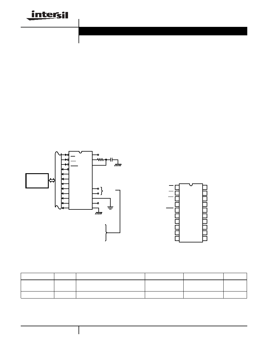
Typical Application Schematic
Features
∑ 80C48 and 80C80/85 Bus Compatible - No Interfacing
Logic Required
∑ Conversion Time . . . . . . . . . . . . . . . . . . . . . . . . . . <100
µ
s
∑ Easy Interface to Most Microprocessors
∑ Will Operate in a "Stand Alone" Mode
∑ Differential Analog Voltage Inputs
∑ Works with Bandgap Voltage References
∑ TTL Compatible Inputs and Outputs
∑ On-Chip Clock Generator
∑ Analog Voltage Input Range
(Single + 5V Supply) . . . . . . . . . . . . . . . . . . . . . . 0V to 5V
∑ No Zero-Adjust Required
∑ 80C48 and 80C80/85 Bus Compatible - No Interfacing
Logic Required
Pinout
ADC0803, ADC0804
(PDIP)
TOP VIEW
3
2
1
12
11
5
15
14
13
18
17
16
7
6
10
9
8
4
19
20
WR
RD
CS
DB
6
DB
7
INTR
DB
3
DB
4
DB
5
DB
0
DB
1
DB
2
CLK IN
CLK R
V+
V
IN
(-)
V
IN
(+)
DGND
V
REF
/2
AGND
ANY
µ
PROCESSOR
8-BIT RESOLUTION
OVER ANY
DESIRED
ANALOG INPUT
VOLTAGE RANGE
DIFF
INPUTS
10K
150pF
V
REF
/2
µ
P BUS
+5V
11
12
13
14
15
16
17
18
20
19
10
9
8
7
6
5
4
3
2
1
WR
RD
CS
CLK IN
INTR
V
IN
(-)
V
IN
(+)
DGND
V
REF
/2
AGND
V+ OR V
REF
CLK R
DB
0 (LSB)
DB
1
DB
2
DB
3
DB
4
DB
5
DB
6
DB
7 (MSB)
Ordering Information
PART NUMBER
ERROR
EXTERNAL CONDITIONS
TEMP. RANGE (
o
C)
PACKAGE
PKG. NO
ADC0803LCN
±
1
/
2
LSB
V
REF
/2 Adjusted for Correct Full Scale
Reading
0 to 70
20 Ld PDIP
E20.3
ADC0804LCN
±
1 LSB
V
REF
/2 = 2.500V
DC
(No Adjustments)
0 to 70
20 Ld PDIP
E20.3
Data Sheet
August 2002
CAUTION: These devices are sensitive to electrostatic discharge; follow proper IC Handling Procedures.
1-888-INTERSIL or 321-724-7143
|
Intersil (and design) is a registered trademark of Intersil Americas Inc.
Copyright © Intersil Americas Inc. 2002. All Rights Reserved
2
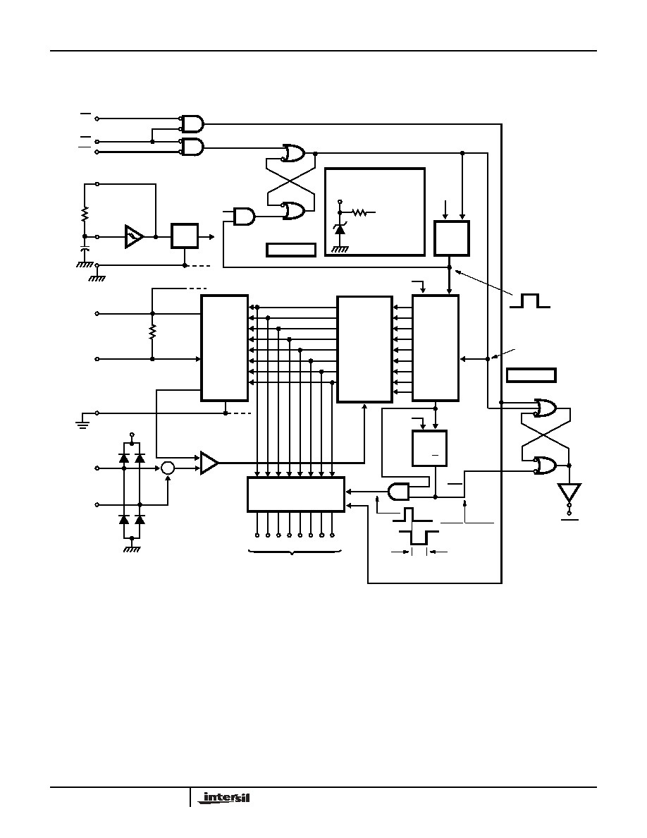
Functional Diagram
12
11
15
14
13
18
17
16
WR
RD
CS
INTR
CLK OSC
CLK R
V+
V
IN
(-)
V
IN
(+)
DGND
V
REF
/2
AGND
(V
REF
)
DAC
V
OUT
COMP
CLK
GEN CLKS
CLK A
RESET
START F/F
LADDER
AND
DECODER
SUCCESSIVE
APPROX.
REGISTER
AND LATCH
8-BIT
SHIFT
REGISTER
D
RESET
SET
CONV. COMPL.
THREE-STATE
OUTPUT LATCHES
DIGITAL OUTPUTS
THREE-STATE CONTROL
"1" = OUTPUT ENABLE
DFF2
CLK A
XFER
G2
Q
8 X 1/f
R
Q
INTR F/F
IF RESET = "0"
D
DFF1
Q
D
Q
CLK B
START
CONVERSION
MSB
LSB
Q
"1" = RESET SHIFT REGISTER
"0" = BUSY AND RESET STATE
RESET
READ
SET
3
2
1
5
7
6
10
9
8
4
19
20
CLK IN
MSB
G1
CLK
-
+
LSB
INPUT PROTECTION
FOR ALL LOGIC INPUTS
INPUT
TO INTERNAL
BV = 30V
CIRCUITS
V+
+
-
ADC0803, ADC0804
3
Absolute Maximum Ratings
Thermal Information
Supply Voltage . . . . . . . . . . . . . . . . . . . . . . . . . . . . . . . . . . . . . . 6.5V
Voltage at Any Input. . . . . . . . . . . . . . . . . . . . . . -0.3V to (V
+
+0.3V)
Operating Conditions
Temperature Range . . . . . . . . . . . . . . . . . . . . . . . . . . . . 0
o
C to 70
o
C
Thermal Resistance (Typical, Note 1)
JA
(
o
C/W)
PDIP Package . . . . . . . . . . . . . . . . . . . . . . . . . . . . .
80
Maximum Junction Temperature
Plastic Package . . . . . . . . . . . . . . . . . . . . . . . . . . . . . . . . . .150
o
C
Maximum Storage Temperature Range . . . . . . . . . . -65
o
C to 150
o
C
Maximum Lead Temperature (Soldering, 10s). . . . . . . . . . . . .300
o
C
CAUTION: Stresses above those listed in "Absolute Maximum Ratings" may cause permanent damage to the device. This is a stress only rating and operation of the
device at these or any other conditions above those indicated in the operational sections of this specification is not implied.
NOTE:
1.
JA
is measured with the component mounted on a low effective thermal conductivity test board in free air. See Tech Brief TB379 for details.
Electrical Specifications
(Notes 2, 8)
PARAMETER
TEST CONDITIONS
MIN
TYP
MAX
UNITS
CONVERTER SPECIFICATIONS V+ = 5V, T
A
= 25
o
C and f
CLK
= 640kHz, Unless Otherwise Specified
Total Unadjusted Error
ADC0803
V
REF
/2 Adjusted for Correct Full Scale Reading
-
-
±
1
/
2
LSB
ADC0804
V
REF
/2 = 2.500V
-
-
±
1
LSB
V
REF
/2 Input Resistance
Input Resistance at Pin 9
1.0
1.3
-
k
Analog Input Voltage Range
(Note 3)
GND-0.05
-
(V+) + 0.05
V
DC Common-Mode Rejection
Over Analog Input Voltage Range
-
±
1
/
16
±
1
/
8
LSB
Power Supply Sensitivity
V+ = 5V
±
10% Over Allowed Input Voltage
Range
-
±
1
/
16
±
1
/
8
LSB
CONVERTER SPECIFICATIONS V+ = 5V, 0
o
C to 70
o
C and f
CLK
= 640kHz, Unless Otherwise Specified
Total Unadjusted Error
ADC0803
V
REF
/2 Adjusted for Correct Full Scale Reading
-
-
±
1
/
2
LSB
ADC0804
V
REF
/2 = 2.500V
-
-
±
1
LSB
V
REF
/2 Input Resistance
Input Resistance at Pin 9
1.0
1.3
-
k
Analog Input Voltage Range
(Note 3)
GND-0.05
-
(V+) + 0.05
V
DC Common-Mode Rejection
Over Analog Input Voltage Range
-
±
1
/
8
±
1
/
4
LSB
Power Supply Sensitivity
V+ = 5V
±
10% Over Allowed Input Voltage
Range
-
±
1
/
16
±
1
/
8
LSB
AC TIMING SPECIFICATIONS V+ = 5V, and T
A
=
25
o
C, Unless Otherwise Specified
Clock Frequency, f
CLK
V+ = 6V (Note 4)
100
640
1280
kHz
V+ = 5V
100
640
800
kHz
Clock Periods per Conversion (Note 5),
t
CONV
62
-
73
Clocks/Conv
Conversion Rate In Free-Running Mode, CR INTR tied to WR with CS = 0V, f
CLK
= 640kHz
-
-
8888
Conv/s
Width of WR Input (Start Pulse Width),
t
W(WR)I
CS = 0V (Note 6)
100
-
-
ns
Access Time (Delay from Falling Edge of
RD to Output Data Valid), t
ACC
C
L
= 100pF (Use Bus Driver IC for Larger C
L)
-
135
200
ns
Three-State Control (Delay from Rising
Edge of RD to Hl-Z State), t
1H
, t
0H
C
L
= 10pF, R
L
= 10K
(See Three-State Test Circuits)
-
125
250
ns
Delay from Falling Edge of WR to Reset of
INTR, t
WI
, t
RI
-
300
450
ns
Input Capacitance of Logic Control Inputs,
C
IN
-
5
-
pF
Three-State Output Capacitance (Data
Buffers), C
OUT
-
5
-
pF
ADC0803, ADC0804

4
DC DIGITAL LEVELS AND DC SPECIFICATIONS V+ = 5V, and T
MIN
to T
MAX
, Unless Otherwise Specified
CONTROL INPUTS (Note 7)
Logic "1" Input Voltage (Except Pin 4 CLK
IN), V
INH
V+ = 5.25V
2.0
-
V+
V
Logic "0" Input Voltage (Except Pin 4 CLK
IN), V
INL
V+
= 4.75V
-
-
0.8
V
CLK IN (Pin 4) Positive Going Threshold
Voltage, V+
CLK
2.7
3.1
3.5
V
CLK IN (Pin 4) Negative Going Threshold
Voltage, V-
CLK
1.5
1.8
2.1
V
CLK IN (Pin 4) Hysteresis, V
H
0.6
1.3
2.0
V
Logic "1" Input Current (All Inputs), I
INHI
V
lN
= 5V
-
0.005
1
µ
Logic "0" Input Current (All Inputs), I
INLO
V
lN
= 0V
-1
-0.005
-
µ
A
Supply Current (Includes Ladder Current), I+ f
CLK
= 640kHz, T
A
= 25
o
C and CS = Hl
-
1.3
2.5
mA
DATA OUTPUTS AND INTR
Logic "0" Output Voltage, V
OL
l
O
= 1.6mA, V+ = 4.75V
-
-
0.4
V
Logic "1" Output Voltage, V
OH
l
O
= -360
µ
A, V+ = 4.75V
2.4
-
-
V
Three-State Disabled Output Leakage (All
Data Buffers)
, I
LO
V
OUT
= 0V
-3
-
-
µ
A
V
OUT
= 5V
-
-
3
µ
A
Output Short Circuit Current, I
SOURCE
V
OUT
Short to GND, T
A
= 25
o
C
4.5
6
-
mA
Output Short Circuit Current, I
SINK
V
OUT
Short to V+, T
A
= 25
o
C
9.0
16
-
mA
NOTES:
2. All voltages are measured with respect to GND, unless otherwise specified. The separate AGND point should always be wired to the DGND,
being careful to avoid ground loops.
3. For V
IN(-)
V
IN(+)
the digital output code will be 0000 0000. Two on-chip diodes are tied to each analog input (see Block Diagram) which will
forward conduct for analog input voltages one diode drop below ground or one diode drop greater than the V+ supply. Be careful, during testing
at low V+ levels (4.5V), as high level analog inputs (5V) can cause this input diode to conduct - especially at elevated temperatures, and cause
errors for analog inputs near full scale. As long as the analog V
IN
does not exceed the supply voltage by more than 50mV, the output code will
be correct. To achieve an absolute 0V to 5V input voltage range will therefore require a minimum supply voltage of 4.950V over temperature
variations, initial tolerance and loading.
4. With V+ = 6V, the digital logic interfaces are no longer TTL compatible.
5. With an asynchronous start pulse, up to 8 clock periods may be required before the internal clock phases are proper to start the conversion process.
6. The CS input is assumed to bracket the WR strobe input so that timing is dependent on the WR pulse width. An arbitrarily wide pulse width will
hold the converter in a reset mode and the start of conversion is initiated by the low to high transition of the WR pulse (see Timing Diagrams).
7. CLK IN (pin 4) is the input of a Schmitt trigger circuit and is therefore specified separately.
8. None of these A/Ds requires a zero-adjust. However, if an all zero code is desired for an analog input other than 0V, or if a narrow full scale span exists
(for example: 0.5V to 4V full scale) the V
IN(-)
input can be adjusted to achieve this. See the Zero Error description in this data sheet.
Electrical Specifications
(Notes 2, 8) (Continued)
PARAMETER
TEST CONDITIONS
MIN
TYP
MAX
UNITS
Timing Waveforms
FIGURE 1A. t
1H
FIGURE 1B. t
1H
, C
L
= 10pF
10K
V+
RD
CS
C
L
DATA
OUTPUT
RD
2.4V
t
r
90%
50%
10%
t
1H
0.8V
DATA
OUTPUTS
GND
t
r
= 20ns
V
OH
90%
ADC0803, ADC0804

5
FIGURE 1C. t
0H
FIGURE 1D. t
0H
, C
L
= 10pF
FIGURE 1. THREE-STATE CIRCUITS AND WAVEFORMS
Timing Waveforms
(Continued)
10K
V+
RD
CS
C
L
DATA
OUTPUT
V+
RD
2.4V
t
r
90%
50%
10%
t
0H
0.8V
DATA
OUTPUTS
V
OI
t
r
= 20ns
V+
10%
Typical Performance Curves
FIGURE 2. LOGIC INPUT THRESHOLD VOLTAGE vs SUPPLY
VOLTAGE
FIGURE 3. DELAY FROM FALLING EDGE OF RD TO OUTPUT
DATA VALID vs LOAD CAPACITANCE
FIGURE 4. CLK IN SCHMITT TRIP LEVELS vs SUPPLY
VOLTAGE
FIGURE 5. f
CLK
vs CLOCK CAPACITOR
-55
o
C TO 125
o
C
1.8
1.7
1.6
1.5
1.4
1.3
4.75
4.50
5.00
5.25
5.50
V+ SUPPLY VOLTAGE (V)
L
O
GIC INPUT THRES
H
OLD V
O
L
T
AGE
(V
)
DE
LA
Y (ns)
500
400
300
200
100
0
LOAD CAPACITANCE (pF)
200
400
600
800
1000
CL
K IN
THRESHOL
D VOL
T
A
GE (V)
3.5
3.1
2.7
2.3
1.9
1.5
4.50
V+ SUPPLY VOLTAGE (V)
-55
o
C TO 125
o
C
V
T(-)
V
T(+)
4.75
5.00
5.25
5.50
1000
CLOCK CAPACITOR (pF)
f
CL
K
(kHz)
100
100
10
1000
R = 10K
R = 50K
R = 20K
ADC0803, ADC0804