 | –≠–ª–µ–∫—Ç—Ä–æ–Ω–Ω—ã–π –∫–æ–º–ø–æ–Ω–µ–Ω—Ç: AN1077 | –°–∫–∞—á–∞—Ç—å:  PDF PDF  ZIP ZIP |

1
Æ
ISL6244EVAL1 Multi-phase Evaluation Board
Setup Procedure
This document describes the setup procedure for the
ISL6244EVAL1 Rev B board for AMD Mobile K8 Processors.
Description
The AMD Hammer family microprocessors feature higher
clock speeds and greater device density than previous
product families. The power management solution for this
next generation family of microprocessors must contend with
lower core voltages, tighter transient specifications, and
higher peak current demands. Responding to the changing
power management needs of its customers, Intersil
introduces the ISL6244 controller to power the AMD
Hammer family microprocessors.
Intersil ISL6244 and ISL6207
The ISL6244EVAL1 Rev B is a versatile voltage regulator-
down (VRD) design. The evaluation board comes configured
for 3-phase multi-phase buck operation, designed to meet
AMD Hammer Family Desktop Processor specifications. The
board layout supports removal or addition of the third and
fourth phases to support multiple applications. The ISL6244
controller features are specifically designed to compliment
and support the Hammer Family processors. Interfaced with
ISL6207 drivers, the chipset forms a highly integrated
solution for AMD Hammer processor applications.
The ISL6244 regulates output voltage and balances load
currents for two to four synchronous buck converter
channels. The controller features a 5-bit DAC which provides
a digital interface for accurate step down conversion over
the entire Hammer Family range of 0.800V to 1.550V. New
multi-phase family features include differential remote output
voltage sensing to improve regulation tolerance, pin-
adjustable reference offset for ease of implementation, VID-
on-the-Fly to respond to DAC changes during operation, and
optional load line regulation. For a more detailed description
of the ISL6244 functionality, refer to the data sheet [1].
The ISL6207 driver is chosen to drive two N-Channel power
MOSFETs in a synchronous-rectified buck converter
channel. Each channel has a single logic input which
controls the upper and lower MOSFETs. Dead time is
optimized on both switching edges to provide shoot-thru
protection. Internal bootstrap circuitry only requires an
external capacitor and provides better enhancement of the
upper MOSFET. For a more detailed description of the
ISL6207, refer to the data sheet [1].
The Intersil multi-phase family driver portfolio continues to
expand with new selections to better fit our customer's
needs.
1. Refer to our website for updated information, the ISL6207 data
sheet, and the ISL6244 data sheet: www.intersil.com.
Features
∑ Multi-Phase Power Conversion
- 2, 3 or 4 Phase Operation
∑ Precision r
DS(ON)
Current Sharing
- Lossless
- Low Cost
∑ Precision CORE Voltage Regulation
- Differential Remote Output Voltage Sensing
- Programmable Reference Offset
- ±
1
% System Accuracy
∑ Programmable Droop Voltage
∑ Excellent Dynamic Response
- Combined Input Voltage Feed-Forward and Pulse-by-
Pulse Average Current Mode
Pinout
ISL6244CR
(32 LEAD QFN 5X5)
TOP VIEW
Ordering Information
PART NUMBER TEMP. (
o
C)
PACKAGE
PKG. DWG. #
ISL6244CR
0 to 70
32 Ld QFN
L32.5X5
ISL6244CRZ
0 to 70
32 Lead-Free QFN
L32.5X5
ISL6244HR
-10 to 100 32 Ld QFN
L32.5X5
ISL6244HRZ
-10 to 100 32 Lead-Free QFN
L32.5X5
NOTE: Add "-T" suffix for 32 QFN 5x5 Tape and Reel packages.
NC = NO CONNECT
1
2
3
4
5
6
7
8
24
23
22
21
20
19
18
17
32
31
30
29
28
27
26
25
9
10
11
12
13
14
15
16
VID2
VID1
VID0
NC
OFS
COMP
FB
NC
ISEN3
ISEN2
GND
PWM2
PWM1
ISEN1
ISEN4
PWM4
PG
O
O
D
FS
EN
GND
VFF
VI
D4
NC
VI
D
3
IO
UT
VDI
F
F
VS
EN
RGND
GND
GND
VCC
PW
M
3
September 2003
AN1077
Application Note
CAUTION: These devices are sensitive to electrostatic discharge; follow proper IC Handling Procedures.
1-888-INTERSIL or 321-724-7143
|
Intersil (and design) is a registered trademark of Intersil Americas Inc.
Copyright © Intersil Americas Inc. 2003. All Rights Reserved
All other trademarks mentioned are the property of their respective owners.

2
Application Note 1077
What's Inside
The Evaluation Board Kit contains the following materials:
∑ The ISL6244 EVAL Board
∑ The ISL6244 Evaluation Board document
What is Needed
The following materials will be needed to perform testing:
∑ 1 to 2 electronic loads [see note]
≠ 0-25V @ 15A (+VDC)
≠ 0-5V @ 5A (+5V)
≠ 0-12V @ 1A (+12V)
∑ precision digital multi-meters
NOTE: amperage rating of power supplies are determined by
maximum expected loading plus a percentage margin of error
Quick Setup Guide
Step 1:
Set the 0-5V power supply to +5V and place in the
"STANDBY" or "OFF" position. Connect the
positive terminal (+) of the supply to the +5V
terminal J5 and the negative terminal (-) of the
supply to GND J7.
Step 2:
Connect the positive terminal (+) of a DMM to the
+5V terminal J5 and the negative terminal (-) to the
GND terminal J7.
Step 3:
Set the +VDC power supply to +19V and place in
the "STANDBY" or "OFF" position. Connect the
positive terminal (+) of the supply to the +VDC
terminal J3 and the negative terminal (-) of the
supply to GND J4.Connect the load
Step 4:
Connect the positive terminal (+) of a DMM to the
+VDC terminal J3 and the negative terminal (-) to
the GND terminal J4.
Step 5:
Set the 0-12V power supply to +12V and place in
the "STANDBY" or "OFF" position. Connect the
positive terminal (+) of the supply to the +12V
terminal J6 and the negative terminal (-) of the
supply to GND J8.
Step 6:
Connect the positive terminal (+) of a DMM to the
+5V terminal J5 and the negative terminal (-) to the
GND terminal J7.
Step 7:
Connect the positive terminal (+) of the electronic
load to the VOUT terminal J1. Connect the
negative terminal (-) of the electronic load to the
GND terminal J2. Make sure the electronic load is
set to the 0A condition.
Step 8:
Connect the positive terminal (+) of a DMM to the
VOUT test point TP13 and the negative terminal (-)
to the GND test point TP14.
Step 9:
Check to ensure all jumpers and switches are in
their default positions prior to application of power
(refer to"Detailed Description of Jumper Settings"
and "Detailed Description of Switch Settings" ).
Step 10: Set all power supplies to the "ON" position. LED
CR1 should show Red. Check all DMM displays for
correct voltage levels. Adjust if necessary.
Step 11: Turn the ENABLE switch SW2 to the "ON" position.
LED CR1 should show Green. The VOUT DMM
should read 1.60V (
±
1%).
At this point the board has been properly powered up.
Normal testing can begin.
NOTE: If you need technical assistance, or other assistance, with
the ISL6244 Evaluation Board, call 1-888-INTERSIL (468-3774).
Detailed Description of Jumper Settings
Detailed Description of Switch Settings
JUMPER
POSITION
FUNCTION
JP1
Shunted
Berg Jumper for VCORE Set Point
JUMPER
POSITION
FUNCTION
SW1
On
ENABLE On-Board Load Transient
Off (default)
DISABLE On-Board Load Transient
SW2
On
ENABLE ISL6244 and ISL6207
Off(default)
DISABLE ISL6244 and ISL6207
3
Application Note 1077
ISL6244
CONTROLLER
SW2 (ENABLE SWITCH) = OFF
JP1
SW1 (LOAD TRANSIENT SWITCH) = OFF
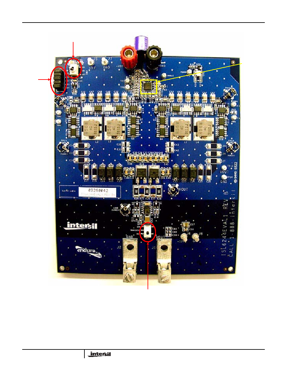
FIGURE 1. ISL6244 EVAL BOARD INITIAL JUMPER AND SWITCH SETTINGS
5 BIT VID
JUMPERS =
SHUNTED
4
Application Note 1077
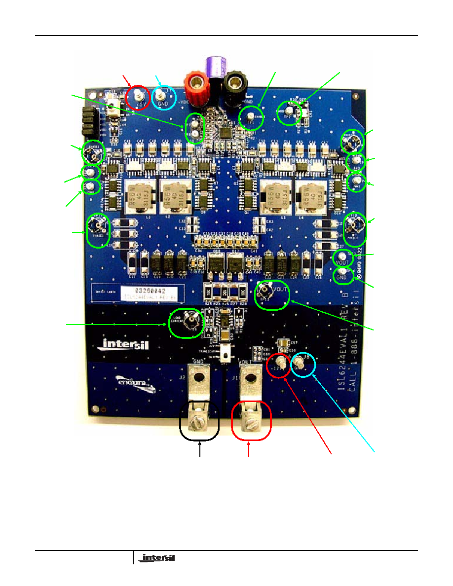
FIGURE 2. ISL6244 EVAL BOARD TEST POINTS
TEST POINT
FOR PWM1
TEST POINT
FOR PWM2
SCOPE JACK
FOR PHASE2
MONITORING
SCOPE JACK
FOR PHASE3
MONITORING
SCOPE JACK
FOR ON-BOARD
LOAD TRANSIENT
CURRENT
MEASUREMENT
SCOPE JACK
FOR VOUT
MONITORING
TEST POINT
FOR VCORE
REMOTE SENSE
TEST POINT
FOR VCORE
REMOTE SENSE
SCOPE JACK
FOR PHASE4
MONITORING
SCOPE JACK
FOR PHASE4
MONITORING
TEST POINT
FOR PWM1
TEST POINT
FOR PWM2
SPECTRUM ANALYZER
FOR LOOP
MEASUREMENT
INPUT
GAIN/PHASE
+5V
VCC INPUT
SOURCE
GND
VCC INPUT
RETURN
J3
+VDC
J4
GND
+12V
INPUT
SOURCE
+12V
INPUT
RETURN
J6
J8
POSITIVE CONNECTION
FOR ELECTRONIC LOAD
+
NEGATIVE CONNECTION
FOR ELECTRONIC LOAD
≠
TEST POINT FOR
ENABLE SENSE
TEST POINT FOR
PGOOD SENSE

5
Application Note 1077
Board Layout Information
5
5
4
4
3
3
2
2
1
1
D
D
C
C
B
B
A
A
0
+VDC
+5V
0
0
0
0
+5V
VCORE-
ISEN1
PWM2
VCORE+
PGOOD
PWM4
ISEN2
PWM1
ISEN3
PWM3
ENABLE
ISEN4
VID4
VID3
VID2
VID1
VID0
Title
Size
Rev
Date:
Sheet
of
B
ISL6244 EVAL 1 for AMD Hammer
A
1
5
Tuesday, June 17, 2003
4020 Stirrup Creek Drive
Durham, NC 27703
Steve Laur
Use to switch between
3 & 4-phase operation:
4-phase: pop R42 (0-ohm)
nopop R41
3-phase: nopop R42
pop R41 (0-ohm)
C1
0.1uF
C3
nopop
TP6
1
TP8
1
R35
0.0
R6
715
TP5
1
TP1
1
R3
107k
U1
ISL6244CR
1
VID2
2
VID1
3
VID0
4
NC
5
OFS
6
COMP
7
FB
8
NC
9
IOUT
10
VDIFF
11
VSEN
12
RGND
13
GND
14
GND
15
VC
C
16
PW
M3
17
ISEN3
18
ISEN2
19
GND
20
PWM2
21
PWM1
22
ISEN1
23
ISEN4
24
PWM4
25
PGOOD
26
FS
27
EN
28
GND
29
VFF
30
VID4
31
NC
32
VID3
33
PAD
TP4
1
R1
90K
TP2
1
R4
2.5k
R8
603
R36
10k
R9
10.0
R2
10K
TP3
1
R7
20.0
C2
12nF
C5
1uF
R42
nopop
C4
6.8nF
TP7
1
R41
0.0
R5
2.43k
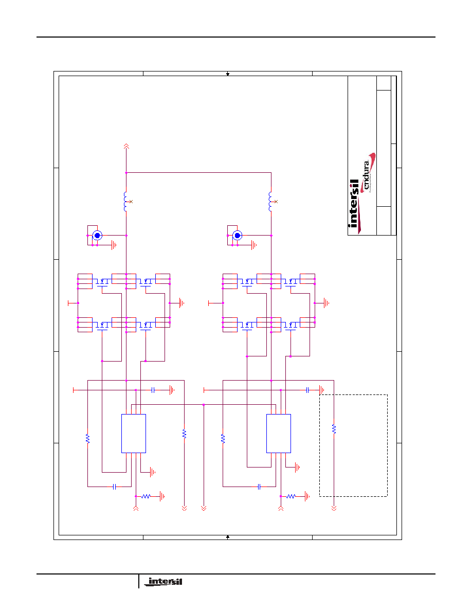
FIGURE 3. SCHEMATIC 1

6
Application Note 1077
Board Layout Information
(Continued)
FIGURE 4. SCHEMATIC 2
5
5
4
4
3
3
2
2
1
1
D
D
C
C
B
B
A
A
0
0
+VDC
+VDC
0
0
+5V
0
0
+5V
0
0
0
0
PWM2
PWM1
VOUT
ISEN2
ISEN1
ENABLE
Title
Size
Rev
Date:
Sheet
of
B
ISL6244 EVAL 1 for AMD Hammer
A
2
5
Wednesday, June 11, 2003
4020 Stirrup Creek Drive
Durham, NC 27703
Steve Laur
R12
0.0
C6
0.1uF
Q8
L2
0.56uH
1
2
3
R13
820PTC
Q6 - nopop
Q1
U3
ISL6207
UGATE
1
BOOT
2
PWM
3
GND
4
LGATE
5
VCC
6
EN
7
PHASE
8
Q7
PHASE2
TP10
Q4
U2
ISL6207
UGATE
1
BOOT
2
PWM
3
GND
4
LGATE
5
VCC
6
EN
7
PHASE
8
Q5
C9
1uF
C8
0.1uF
R37
nopop
L1
0.56uH
1
2
3
R38
nopop
PHASE1
TP9
Q3
R11
820PTC
C7
1uF
R10
0.0
Q2 - nopop
7
Application Note 1077
Board Layout Information
(Continued)
5
5
4
4
3
3
2
2
1
1
D
D
C
C
B
B
A
A
0
0
+VDC
+VDC
0
0
+5V
+5V
0
0
0
0
0
0
ISEN3
ISEN4
PWM4
PWM3
ENABLE
VOUT
Title
Size
Rev
Date:
Sheet
of
B
ISL6244 EVAL 1 for AMD Hammer
A
3
5
Tuesday, June 17, 2003
4020 Stirrup Creek Drive
Durham, NC 27703
Steve Laur
Use to switch between
3 & 4-phase operation:
4-phase: pop R17 (820-PTC)
3-phase: nopop R17
Q15
C12
0.1uF
R14
0.0
U5
ISL6207
UGATE
1
BOOT
2
PWM
3
GND
4
LGATE
5
VCC
6
EN
7
PHASE
8
R40
nopop
Q10 - nopop
R17
nopop
Q11
PHASE3
TP11
U4
ISL6207
UGATE
1
BOOT
2
PWM
3
GND
4
LGATE
5
VCC
6
EN
7
PHASE
8
Q14 - nopop
L3
0.56uH
1
2
3
C13
1uF
R39
nopop
R16
0.0
Q9
Q16
C10
0.1uF
L4
0.56uH
1
2
3
C11
1uF
Q12
PHASE4
TP12
Q13
R15
820PTC
FIGURE 5. SCHEMATIC 3

8
Application Note 1077
Board Layout Information
(Continued)
5
5
4
4
3
3
2
2
1
1
D
D
C
C
B
B
A
A
0
+VDC
0
+5V
0
0
VOUT
+12V
Title
Size
Rev
Date:
Sheet
of
B
ISL6244 EVAL 1 for AMD Hammer
A
4
5
Monday, July 14, 2003
4020 Stirrup Creek Drive
Durham, NC 27703
Steve Laur
Output Capacitance
Input Capacitance
+5V decoupling
(locate by power terminals)
+12V decoupling
(locate by power terminals)
C29
nopop
C36
22uF
C58
1uF
C48
10uF
C51
10uF
C42
nopop
C16
nopop
C39
22uF
C41
22uF
C46
10uF
C21
330uF
J5
+5V
C26
nopop
J4
GND
C31
22uF
C54
10uF
C66
10uF
C34
22uF
C55
10uF
C30
22uF
C45
22uF
C18
nopop
C28
nopop
C37
22uF
C23
330uF
TP14
1
C49
10uF
C15
nopop
C40
22uF
C24
330uF
J7
GND
C27
nopop
C52
10uF
C32
nopop
C67
10uF
C20
330uF
TP13
1
C56
1uF
C35
22uF
C17
nopop
J3
+VDC2
J8
GND
C47
10uF
C38
22uF
C50
10uF
J2
GND
C44
22uF
C22
330uF
C57
10uF
J1
VOUT
C25
nopop
C43
nopop
C14
nopop
C53
10uF
C65
10uF
C33
nopop
C19
330uF
J6
+12V
FIGURE 6. SCHEMATIC 4
9
Application Note 1077
Board Layout Information
(Continued)
5
4
D
C
B
0
0
0
0
0
0
0
0
+5V
0
+5V
0
0
0
0
0
VOUT
VCORE+
VCORE-
ENABLE
VOUT
+12V
PGOOD
VID4
VID1
VID2
VID0
VID3
+12V
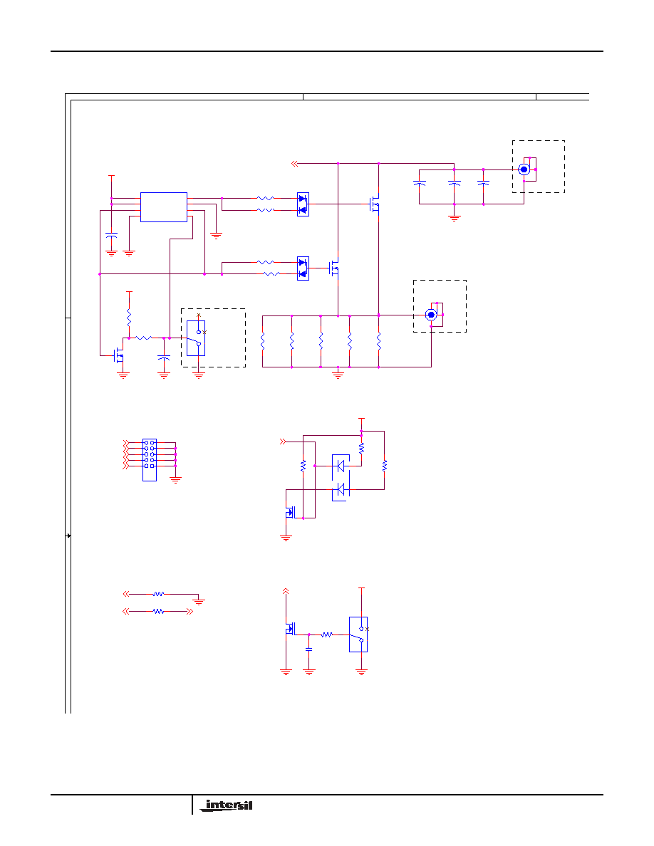
Top Side
Top Side
OFF
TRANSIENT
ON
POWER GOOD
INDICATOR
VID4
VID3
VID2
VID1
VID0
VID CODE
Transient Load Generator
ON
ENABLE VR
OFF
ENABLE SIGNAL
REMOTE SENSE LINES
connect at output caps
VCC_CORE
TP15
R24
.100
C62
1uF
Q18
HUF76129D3S
1
3
2
Q21
2n7002
1
3
2
C60
no pop
JP1
1
3
5
7
9
10
8
6
4
2
C64
1n
R22
46.4k_1%
Q19
2N7002
1
2
3
R18 357_1%
R30
10k
R19 324_1%
R28
.100
SW1
R20 357_1%
R33
0.0
R27
nopop
Q20
2n7002
1
3
2
C61
no pop
LOAD CURRENT
TP16
SW2
U6
HIP2100
VDD
1
HB
2
HO
3
HS
4
HI
5
LI
6
VSS
7
LO
8
Q17
HUF76129D3S
1
3
2
R23 402_1%
R26
nopop
D1
D2
R29
2.43k
R32
0.0
RE
D
G
RE
E
N
CR1
1
3
2
4
R21 324_1%
R34
10k
C59
no pop
R25
nopop
C63
10uF
R31
2.43k
FIGURE 7. SCHEMATIC 5

10
Application Note 1077
TABLE 1. BILL OF MATERIALS
ITEM
QTY
REFERENCE
VALUE
TYPE
FOOTPRINT
VOLTAGE*
1
1
CR1
Dual LED2
DIGIKEY 67-1372-1-ND
smdp_led_gw
-
2
18
C3, C59, C60, C61, C14-C18, Q2, Q6,
Q10, Q14, C25-C29, R25, R26, R27,
R37, R38, R39, R40, R42, R17
nopop
-
-
-
3
1
C4
7.4nF
-
-
-
4
1
C2
12nF
-
0805
10V
5
7
C5, C7, C9, C11, C56, C58, C13
1
µ
F
-
0805
16V
6
4
C32, C33, C42, C43
nopop
-
1210
10V
7
1
C62
1
µ
F
-
1206
16V
8
4
C1, C6, C8, C10, C12
0.1
µ
F
-
0805
10V
9
16
C19, C20, C21, C22, C23, C24
330
µ
F
Panasonic EEFSE0E331R
7343
-
10
12
C30, C31, C34-C41, C44, C45
22
µ
F
Panasonic: ECJ3YB0J226M
1206
6.3V
11
14
C46, C47, C48, C49, C50, C51, C52,
C53, C54, C55, C57, C65, C66, C67
10
µ
F
Taiyo Yuden TMK325F106ZH
1210
25V
12
1
C63
10
µ
F
Taiyo Yuden TMK325F106ZH
1812
25V
13
1
C64
1n
-
0805
10V
14
2
D1, D2
BAV99LT1
BAV99LT1
SOT23
-
15
1
JP1
Jumper - 5Pos
BERG 2x5 100MIL Header
jumper10
-
16
1
J1
VOUT
BURNDY KPA8CTP
kpa8ctp
-
17
1
J2
GND
BURNDY KPA8CTP
kpa8ctp
-
18
1
J3
+VDC
NEWARK 111-0702-001 RED
pad-170
-
19
1
J4
GND
NEWARK 111-0703-001 BLK
pad-170
-
20
1
J5
+5V
DIGIKEY 1514-2K-ND
tp-150c100p
-
21
1
J6
+12V
DIGIKEY 1514-2K-ND
tp-150c100p
-
22
2
J7, J8
GND
DIGIKEY 1514-2K-ND
tp-150c100p
-
23
3
L1, L2, L3, L4
0.56
µ
H
Panasonic PCC-M104L Series
pcc-nx1_nx2_j
-
24
4
Q1, Q5, Q9, Q13
IRF7811W
-
pwrpak_so8_single
-
25
8
Q3, Q4, Q7, Q8, Q11, Q12, Q15
SI4362
-
pwrpak_so8_single
-
Q16
-
-
-
-
26
2
Q18, Q17
HUF76129D3S
-
TO-252AA
-
27
3
Q19, Q20, Q21
2N7002
-
SOT23
-
28
1
R1
90K
-
0603
-
29
4
R2, R30, R34, R36
10K
-
0603
-
30
1
R3
107K
-
0603
-
31
1
R4
2.5K
-
0603
-
32
1
R5
2.43K
-
0603
-
33
1
R6
710
-
0603
-
34
1
R7
20
-
0603
-
35
1
R8
603
-
-
-
36
1
R9
10
-
0603
-

11
Application Note 1077
37
7
R10, R12, R14, R32, R33, R16, R35,
R41
0.0
-
0603
-
38
3
R11, R13, R15
820PTC
Vishay TFPT0805L820F
0805
-
39
2
R18, R20
357_1%
-
0603
-
40
2
R19, R21
324_1%
-
0603
-
41
1
R22
46.4K_1%
-
0603
-
42
1
R23
402_1%
-
0603
-
43
2
R24, R28
0.1
Vishay WSL series
2512
-
44
2
R29, R31
2.43K
0603
-
45
1
SW1
SPDT
C&K SMT DIGIKEY PN
CKN1101CT-ND
gt11sc
-
46
1
SW2
DPST
C&K SMT DIGIKEY PN
CKN1099CT-ND
gt11sc
-
47
10
TP1, TP2, TP3, TP4, TP5, TP6,
Test Point
KEYSTONE 5002
PAD-100
-
TP7, TP8, TP13, TP14
-
-
-
-
48
1
TP9
Phase1
TEK 131-4244-00
TEK 131-4244-00
-
49
1
TP10
Phase2
TEK 131-4244-00
TEK 131-4244-00
-
50
1
TP11
Phase3
TEK 131-4244-00
TEK 131-4244-00
-
51
1
TP12
Phase4
TEK 131-4244-00
TEK 131-4244-00
-
52
1
TP15
VCC_CORE
TEK 131-4244-00
TEK 131-4244-00
-
53
1
TP16
Load Current
TEK 131-4244-00
TEK 131-4244-00
-
54
1
U1
ISL6244CR
Intersil ISL6244
32mlfp_5x5
-
55
4
U2, U3, U4, U5
ISL6207
Intersil ISL6207
soic8
-
56
1
U6
HIP2100
Intersil HIP2100
soic8
-
TABLE 1. BILL OF MATERIALS (Continued)
ITEM
QTY
REFERENCE
VALUE
TYPE
FOOTPRINT
VOLTAGE*

12
Application Note 1077
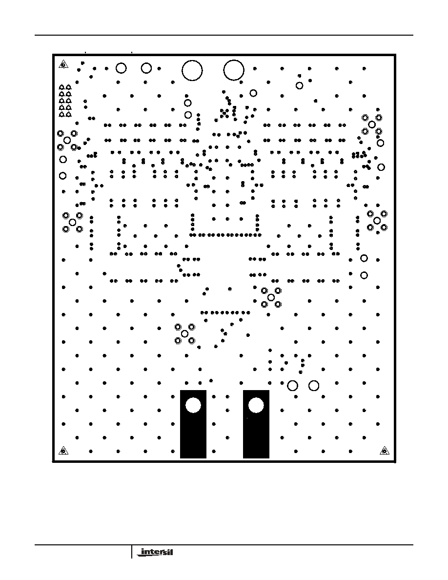
TOP LAYER SILKSCREEN
13
Application Note 1077
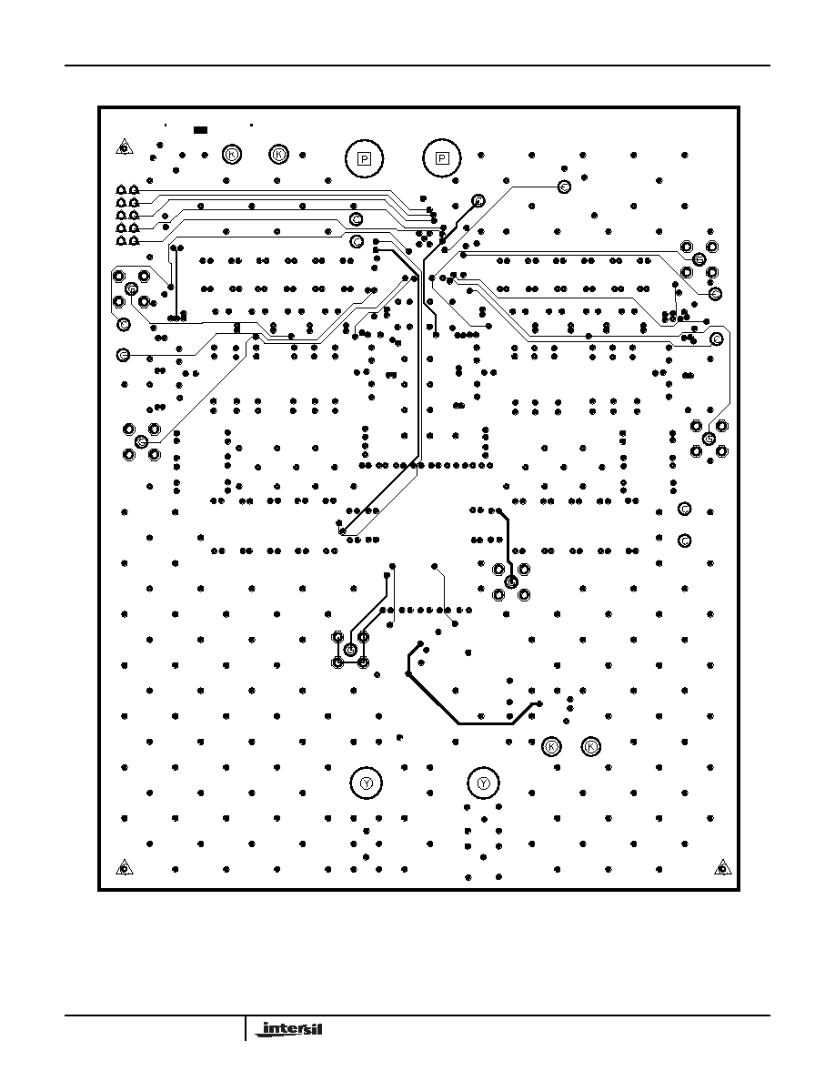
LAYER 2
14
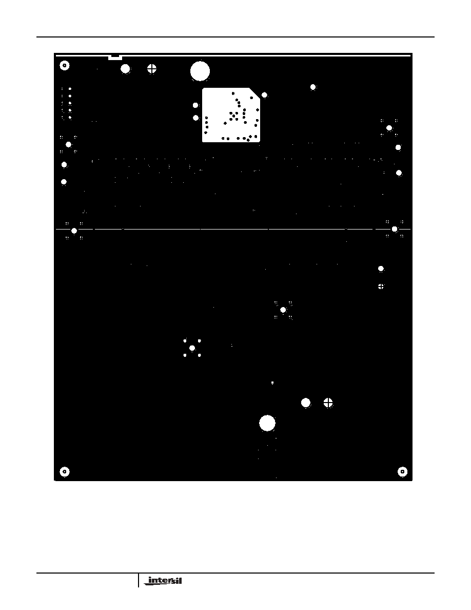
Application Note 1077
LAYER 3
15
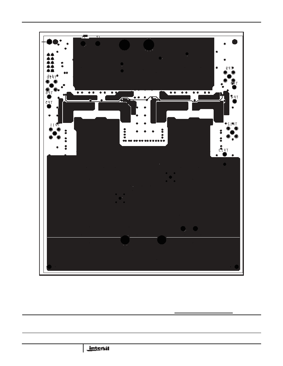
Application Note 1077
LAYER 4
16
All Intersil products are manufactured, assembled and tested utilizing ISO9000 quality systems.
Intersil Corporation's quality certifications can be viewed at website www.intersil.com/design/quality
Intersil products are sold by description only. Intersil Corporation reserves the right to make changes in circuit design and/or specifications at any time without notice.
Accordingly, the reader is cautioned to verify that data sheets are current before placing orders. Information furnished by Intersil is believed to be accurate and reliable. How-
ever, no responsibility is assumed by Intersil or its subsidiaries for its use; nor for any infringements of patents or other rights of third parties which may result from its use.
No license is granted by implication or otherwise under any patent or patent rights of Intersil or its subsidiaries.
For information regarding Intersil Corporation and its products, see web site www.intersil.com
Application Note 1077
BOTTOM SILKSCREEN