 | ÐлекÑÑоннÑй компоненÑ: CA3098E | СкаÑаÑÑ:  PDF PDF  ZIP ZIP |
Äîêóìåíòàöèÿ è îïèñàíèÿ www.docs.chipfind.ru
1
TM
CA3098
Programmable Schmitt Trigger with
Memory, Dual Input Precision Level
Detector
The CA3098 Programmable Schmitt Trigger is a monolithic
silicon integrated circuit designed to control high operating
current loads such as thyristors, lamps, relays, etc. The
CA3098 can be operated with either a single power supply
with maximum operating voltage of 16V, or a dual power
supply with maximum operating voltage of
±
8V. It can
directly control currents up to 150mA and operates with
microwatt standby power dissipation when the current to be
controlled is less than 30mA. The CA3098 contains the
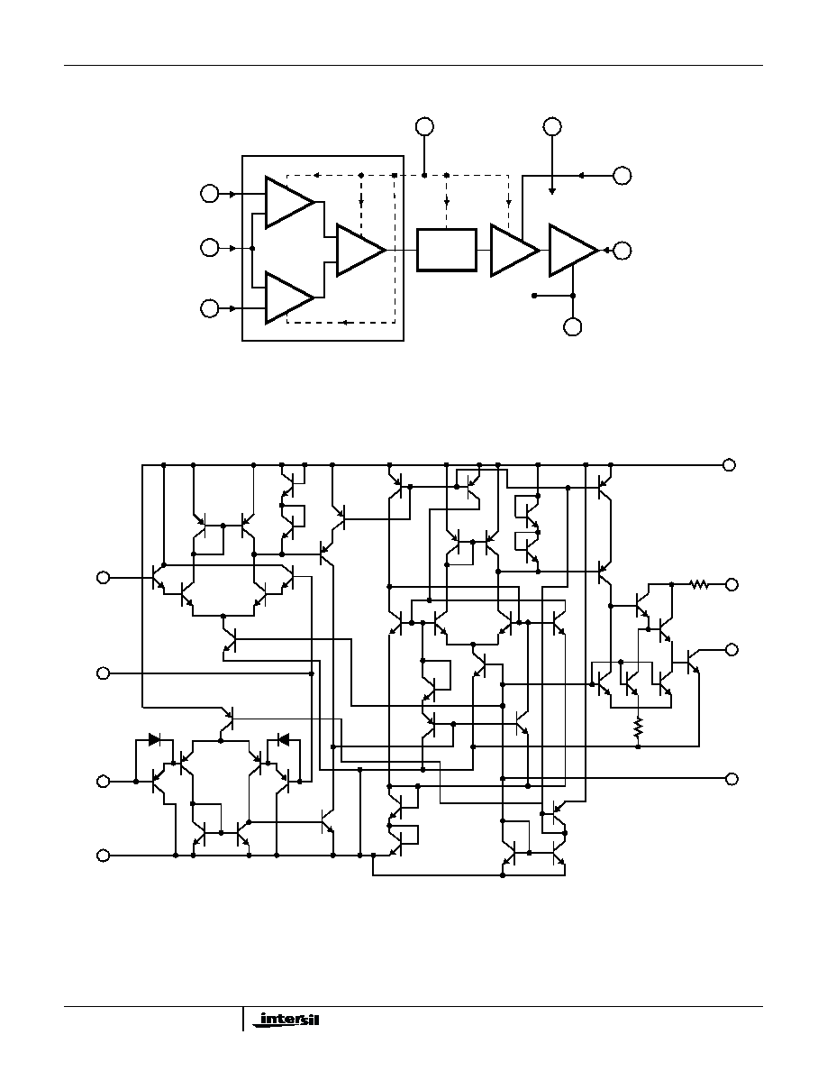
following major circuit function features (see Block Diagram):
1. Differential amplifiers and summer: the circuit uses two
differential amplifiers, one to compare the input voltage
with the "high" reference, and the other to compare the
input with the "low" reference. The resultant output of the
differential amplifiers actuates a summer circuit which
delivers a trigger that initiates a change in state of a flip-
flop.
2. Flip-flop: the flip-flop functions as a bistable "memory"
element that changes state in response to each trigger
command.
3. Driver and output stages: these stages permit the circuit
to "sink" maximum peak load currents up to 150mA at
terminal 3.
4. Programmable operating current: the circuit incorporates
access at terminal 2 to permit programming the desired
quiescent operating current and performance parameters.
Pinout
CA3098
(PDIP)
TOP VIEW
Features
· Programmable Operating Current
· Micropower Standby Dissipation
· Direct Control of Currents Up to . . . . . . . . . . . . . . . 150mA
· Low Input On/Off Current of Less Than 1nA for
Programmable Bias Current of 1
µ
A
· Built-in Hysteresis . . . . . . . . . . . . . . . . . . . . . 20mV (Max)
Applications
· Control of Relays, Heaters, LEDs, Lamps, Photosensitive
Devices, Thyristors, Solenoids, etc.
· Signal Reconditioning
· Phase and Frequency Modulators
· On/Off Motor Switching
· Schmitt Triggers, Level Detectors
· Time Delays
· Overvoltage, Overcurrent, Overtemperature Protection
· Battery-Operated Equipment
· Square and Triangular-Wave Generators
LOW REF.
I
BIAS
OUT
V-
1
2
3
4
8
7
6
5
+IN
HIGH REF.
V+
CURRENT
CONTROL
Part Number Information
PART
NUMBER
TEMP
RANGE (
o
C)
PACKAGE
PKG. NO.
CA3098E
-55 to 125
8 Ld PDIP
E8.3
January 1999
File Number
896.5
)
ma
itt
ith
,
ut
)
()
ds
duc
e,
tor,
t
ent,
le
low
l
ut,
ure
itt
ilt
is,
put
OBS
OLE
TE P
ROD
UCT
NO
REC
OMM
END
ED R
EPL
ACE
MEN
T
Call
1-88
8-IN
TER
SIL
or 3
21-7
24-7
143
CAUTION: These devices are sensitive to electrostatic discharge; follow proper IC Handling Procedures.
1-888-INTERSIL or 321-724-7143
|
Intersil (and design) is a trademark of Intersil Americas Inc.
Copyright © Intersil Americas Inc. 2001. All Rights Reserved
2
Block Diagram
Schematic Diagram
DIFF.
AMP
DIFF.
AMP
7
1
8
SUMMER
"HIGH"
REF. (HR)
SIGNAL
INPUT
"LOW"
REF. (LR)
FLIP-FLOP
(MEMORY)
2
PROGRAMMABLE
BIAS CURRENT
INPUT (I
BIAS
)
DRIVER
OUTPUT
3
5
4
V-
"SINK
OUTPUT"
OUTPUT
CURRENT
CONTROL
SUBSTRATE
6
V+
COMPARATOR
8
7
"LOW"
REF. (LR)
1
4
SIGNAL
INPUT
5
6
3
2
V-
Q
1
"HIGH"
REF. (HR)
Q
2
Q
6
Q
7
Q
3
Q
4
Q
5
Q
9
Q
8
Q
10
Q
11
Q
20
Q
26
Q
16
Q
14
Q
15
Q
12
Q
17
Q
18
Q
19
Q
31
Q
30
Q
27
Q
28
Q
22
Q
23
Q
32
Q
33
Q
29
Q
34
Q
35
Q
36
Q
38
Q
37
Q
25
Q
24
Q
39
Q
40
Q
41
Q
42
Q
46
Q
45
Q
44
Q
43
R
3
50K
R
14
500
"SINK"
PROGRAMMABLE
V+
BIAS CURRENT
INPUT (I
BIAS
)
OUTPUT
CURRENT
CONTROL
OUTPUT
CA3098
3
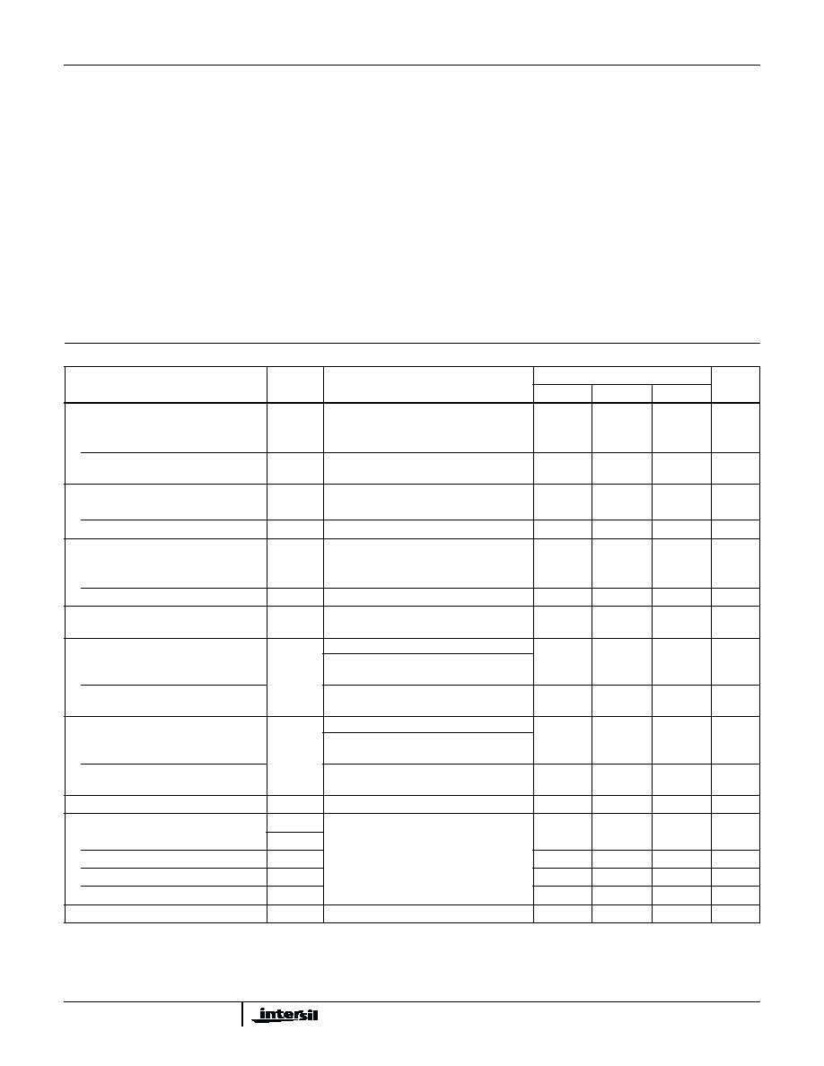
Absolute Maximum Ratings
Thermal Information
Supply Voltage Between V+ and V- . . . . . . . . . . . . . . . . . . . . . . .16V
Voltage Between High Reference or Sink Output and V-. . . . . . .16V
Differential Input Voltage Between Terminals 8 and 1 . . . . . . . . .10V
and Terminals 7 and 8
Load Current (Terminal 3) (Duty Cycle
25%) . . . . . . . . . . . . 150mA
Input Current to Voltage Regulator (Terminal 5) . . . . . . . . . . . 25mA
Programmable Bias Current (Terminal 2) . . . . . . . . . . . . . . . . . 1mA
Output Current Control (Terminal 5). . . . . . . . . . . . . . . . . . . . . 15mA
Operating Conditions
Temperature Range . . . . . . . . . . . . . . . . . . . . . . . . . -55
o
C to 125
o
C
Voltage Range
+IN . . . . . . . . . . . . . . . . . . . . . . . . . . . . . . . . . . . . . . . . . . V- to V+
HIGH REF . . . . . . . . . . . . . . . . . . . . . . . . . . . . . . (V- +2.0V) to V+
LOW REF . . . . . . . . . . . . . . . . . . . . . . . . . . . . . . (V-) to (V+ -2.0V)
Thermal Resistance (Typical, Note 3)
JA
PDIP Package . . . . . . . . . . . . . . . . . . . . . . . . . . . . . .
125
o
C/W
Maximum Junction Temperature (Die). . . . . . . . . . . . . . . . . . . 175
o
C
Maximum Junction Temperature (Plastic Package). . . . . . . . . 150
o
C
Maximum Storage Temperature Range . . . . . . . . . . -65
o
C to 150
o
C
Maximum Lead Temperature (Soldering 10s) . . . . . . . . . . . . 300
o
C
CAUTION: Stresses above those listed in "Absolute Maximum Ratings" may cause permanent damage to the device. This is a stress only rating and operation of the
device at these or any other conditions above those indicated in the operational sections of this specification is not implied.
Electrical Specifications
T
A
= 25
o
C, Unless Otherwise Specified
PARAMETER
SYMBOL
TEST CONDITIONS
CA3098
UNITS
MIN
TYP
MAX
Input Offset Voltage
"Low" Reference (Figures 2, 5)
V
IO(LR)
V
LR
= GND, V
HR
= V+ to (V- +2V),
I
BIAS
= 100
µ
A
-15
-3
6
mV
"High Reference (Figures 2, 6)
V
IO(HR)
V
HR
= GND, V
LR
= V- to (V+ -2V),
I
BIAS
= 100
µ
A
-10
-1
10
mV
Temperature Coefficient
"Low" Reference (Figure 7)
-55
o
C to 125
o
C
-
4.5
-
µ
V/
o
C
"High" Reference (Figure 8)
-55
o
C to 125
o
C
-
±
8.2
-
µ
V/
o
C
Minimum Hysteresis
Voltage (Figure 9)
V
IO(HR-
LR)
V
REG
= 0V (Note 1), V+ = 4V, V- = -4V,
I
BIAS
= 1
µ
A
-
3
20
mV
Temperature Coefficient (Figure 10)
-55
o
C to 125
o
C
-
6.7
-
µ
V/
o
C
Output Saturation Voltage
(Figures 11, 12)
V
CE(SAT)
V
I
= 5V, V
REG
= 6V (Note 1), V+ = 12V,
I
BIAS
= 100
µ
A
-
0.72
1.2
V
Total Supply Current
I
TOTAL
"ON" (Figures 3, 13, 14)
V
I
= 6V, V
REG
> 6V (Note 1), V+ = 16V,
I
BIAS
= 100
µ
A
500
710
800
µ
A
"OFF" (Figures 3, 13, 14)
V
I
= 10V, V
REG
< 10V (Note 1),
V+ = 16V, I
BIAS
= 100
µ
A
400
560
750
µ
A
Input Bias Current (Figures 3, 15)
I
IB
I
B(PNP)
V
I
= 16V, V
REG
< 16V (Note 1),
V+ = 16V, I
BIAS
= 100
µ
A
-
42
100
nA
I
B(NPN)
V
I
= 6V, V
REG
> 6V (Note 1), V+ = 16V,
I
BIAS
= 100
µ
A
-
28
100
nA
Output Leakage Current
I
CE(OFF)
Current from Terminal 3 when Q
46
is "OFF"
-
-
10
µ
A
Switching Times (Figures 4, 16-27)
I
BIAS
= 100
µ
A, V+ = 5V, V
REG
= 2.5V
(Note 1)
Delay Time
tD
-
900
-
ns
Fall Time
tF
-
30
-
ns
Rise Time
tR
-
2000
-
ns
Storage Time
tS
-
6.5
-
µ
s
Output Current (Note 2)
I
O
100
-
-
mA
NOTES:
1. For definition of V
REG
see Figure 3.
2. Continuous (DC) output current must be limited to
40mA. For 100mA output current, the duty cycle must be
40%.
3.
JA
is measured with the component mounted on an evaluation PC board in free air.
CA3098
4
General Description of Circuit Operation
When the signal input voltage of the CA3098 is equal to or
less than the "low" reference voltage (LR), current flows from
an external power supply through a load connected to
Terminal 3 ("sink" output). This condition is maintained until
the signal input voltage rises to or exceeds the "high"
reference voltage (HR), thereby effecting a change in the
state of the flip-flop (memory) such that the output stage
interrupts current flow in the external load. This condition, in
turn, is maintained until such time as the signal again
becomes equal to or less than the "low" reference voltage.
The CA3098 comparator is unique in that it contains circuit
provisions to permit programmability. This feature provides
flexibility to the designer to optimize quiescent power
consumption, input circuit characteristics, hysteresis, and
additionally permits independent control of the comparator,
namely, pulsing, strobing, keying, squelching, etc.
Programmability is accomplished by means of the bias
current (I
BIAS
) supplied to Terminal 2.
An auxiliary means of controlling the magnitude of load
current flow at Terminal 3 is provided by "sinking" current into
Terminal 5. Figure 1 highlights the operation of the CA3098
when connected as a simple hysteresis switch (Schmitt
trigger).
2
6
5
CA3098
I
O
R
L
E
O
V+ = 12V
DC
7
8
1
"LOW" REF. = 4V
"HIGH" REF. = 8V
4
INPUT
SIGNAL
E
IN
120k
R
B
SEQUENCE
INPUT SIGNAL
LEVEL
OUTPUT VOLTAGE (V)
(TERMINAL 3)
1
4
E
IN
> 0
0
2
8
E
IN
> 4
0
3
E
IN
> 8
12
2
8
E
IN
> 4
12
1
4
E
IN
> 0
0
3
FIGURE 1. BASIC HYSTERESIS SWITCH (SCHMITT
TRIGGER) AND RESULTANT OUTPUT STATES
Metallization Mask Layout
Dimensions in parentheses are in millimeters and are derived
from the basic inch dimensions as indicated. Grid graduations
are in mils (10
-3
inch).
The layout represents a chip when it is part of the wafer. When
the wafer is cut into chips, the cleavage angles are 57
o
instead
of 90
o
with respect to the face of the chip. Therefore, the
isolated chip is actually 7mils (0.17mm) larger in both
dimensions.
60
50
40
30
20
10
0
61
0
10
20
30
40
50
58
63 (1.600)
66 (1.676)
CA3098
5
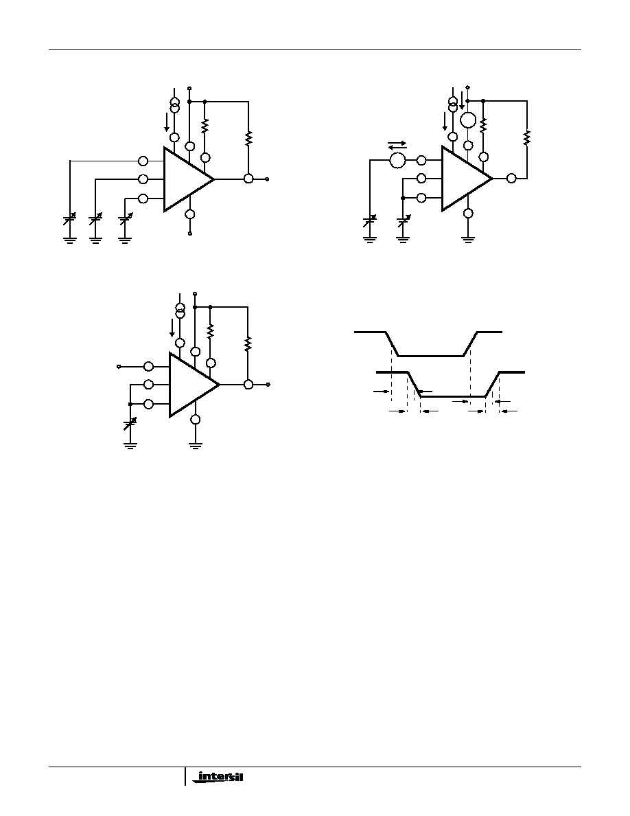
Test Circuits
FIGURE 2. INPUT OFFSET VOLTAGE TEST CIRCUIT
FIGURE 3. TOTAL SUPPLY CURRENT, AND INPUT BIAS
CURRENT TEST CIRCUIT
FIGURE 4. SWITCHING TIME TEST CIRCUIT
2
6
5
CA3098
3
V
O
8
7
1
4
1.5k
-6V
V
LR
V
HR
V
I
I
BIAS
150
+6V
2
6
5
CA3098
3
8
7
1
4
1.1k
V
REG
V
I
I
BIAS
110
V+
mA
mA
I
IB
I
TOTAL
2
6
5
CA3098
8
7
1
4
450
V
REG
I
BIAS
45
V+
V
I
3
V
O
t
D
t
F
t
R
t
S
V
I
V
O
CA3098