5-1
CA3127
High Frequency NPN Transistor Array
Description
The CA3127 consists of five general purpose silicon NPN
transistors on a common monolithic substrate. Each of the
completely isolated transistors exhibits low 1/f noise and a
value of f
T
in excess of 1GHz, making the CA3127 useful
from DC to 500MHz. Access is provided to each of the termi-
nals for the individual transistors and a separate substrate
connection has been provided for maximum application flexi-
bility. The monolithic construction of the CA3127 provides
close electrical and thermal matching of the five transistors.
Ordering Information
PART
NUMBER
(BRAND)
TEMP.
RANGE (
o
C)
PACKAGE
PKG.
NO.
CA3127E
-55 to 125
16 Ld PDIP
E16.3
CA3127M
(3127)
-55 to 125
16 Ld SOIC
M16.15
CA3127M96
(3127)
-55 to 125
16 Ld SOIC Tape and Reel M16.15
Features
� Gain Bandwidth Product (f
T
). . . . . . . . . . . . . . . . >1GHz
� Power Gain . . . . . . . . . . . . . . . . . 30dB (Typ) at 100MHz
� Noise Figure . . . . . . . . . . . . . . . . 3.5dB (Typ) at 100MHz
� Five Independent Transistors on a Common Substrate
Applications
� VHF Amplifiers
� Multifunction Combinations - RF/Mixer/Oscillator
� Sense Amplifiers
� Synchronous Detectors
� VHF Mixers
� IF Converter
� IF Amplifiers
� Synthesizers
� Cascade Amplifiers
August 1996
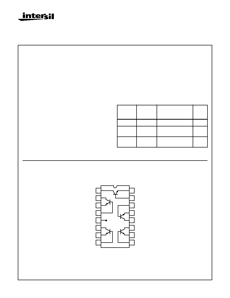
Pinout
CA3127
(PDIP, SOIC)
TOP VIEW
14
15
16
9
13
12
11
10
1
2
3
4
5
7
6
8
SUBSTRATE
Q
2
Q
3
Q
4
Q
5
Q
1
File Number
662.3
CAUTION: These devices are sensitive to electrostatic discharge; follow proper IC Handling Procedures.
1-888-INTERSIL or 321-724-7143 | Copyright � Intersil Corporation 1999
5-2
CA3127
Absolute Maximum Ratings
Thermal Information
The following ratings apply for each transistor in the device
Collector-to-Emitter Voltage, V
CEO
. . . . . . . . . . . . . . . . . . . . . 15V
Collector-to-Base Voltage, V
CBO
. . . . . . . . . . . . . . . . . . . . . . . 20V
Collector-to-Substrate Voltage, V
CIO
(Note 1). . . . . . . . . . . . . 20V
Collector Current, I
C
. . . . . . . . . . . . . . . . . . . . . . . . . . . . . . . 20mA
Operating Conditions
Temperature Range . . . . . . . . . . . . . . . . . . . . . . . . . -55
o
C to 125
o
C
Thermal Resistance (Typical, Note 2)
JA
(
o
C/W)
PDIP Package . . . . . . . . . . . . . . . . . . . . . . . . . . . . .
90
SOIC Package . . . . . . . . . . . . . . . . . . . . . . . . . . . . .
175
Maximum Power Dissipation, P
D
(Any One Transistor). . . . . . 85mW
Maximum Junction Temperature (Die) . . . . . . . . . . . . . . . . . . 175
o
C
Maximum Junction Temperature (Plastic Packages). . . . . . . . 150
o
C
Maximum Storage Temperature Range . . . . . . . . . -65
o
C to 150
o
C
Maximum Lead Temperature (Soldering 10s) . . . . . . . . . . . . . 300
o
C
(SOIC - Lead Tips Only)
CAUTION: Stresses above those listed in "Absolute Maximum Ratings" may cause permanent damage to the device. This is a stress only rating and operation
of the device at these or any other conditions above those indicated in the operational sections of this specification is not implied.
NOTES:
1. The collector of each transistor of the CA3127 is isolated from the substrate by an integral diode. The substrate (Terminal 5) must be con-
nected to the most negative point in the external circuit to maintain isolation between transistors and to provide for normal transistor action.
2.
JA
is measured with the component mounted on an evaluation PC board in free air.
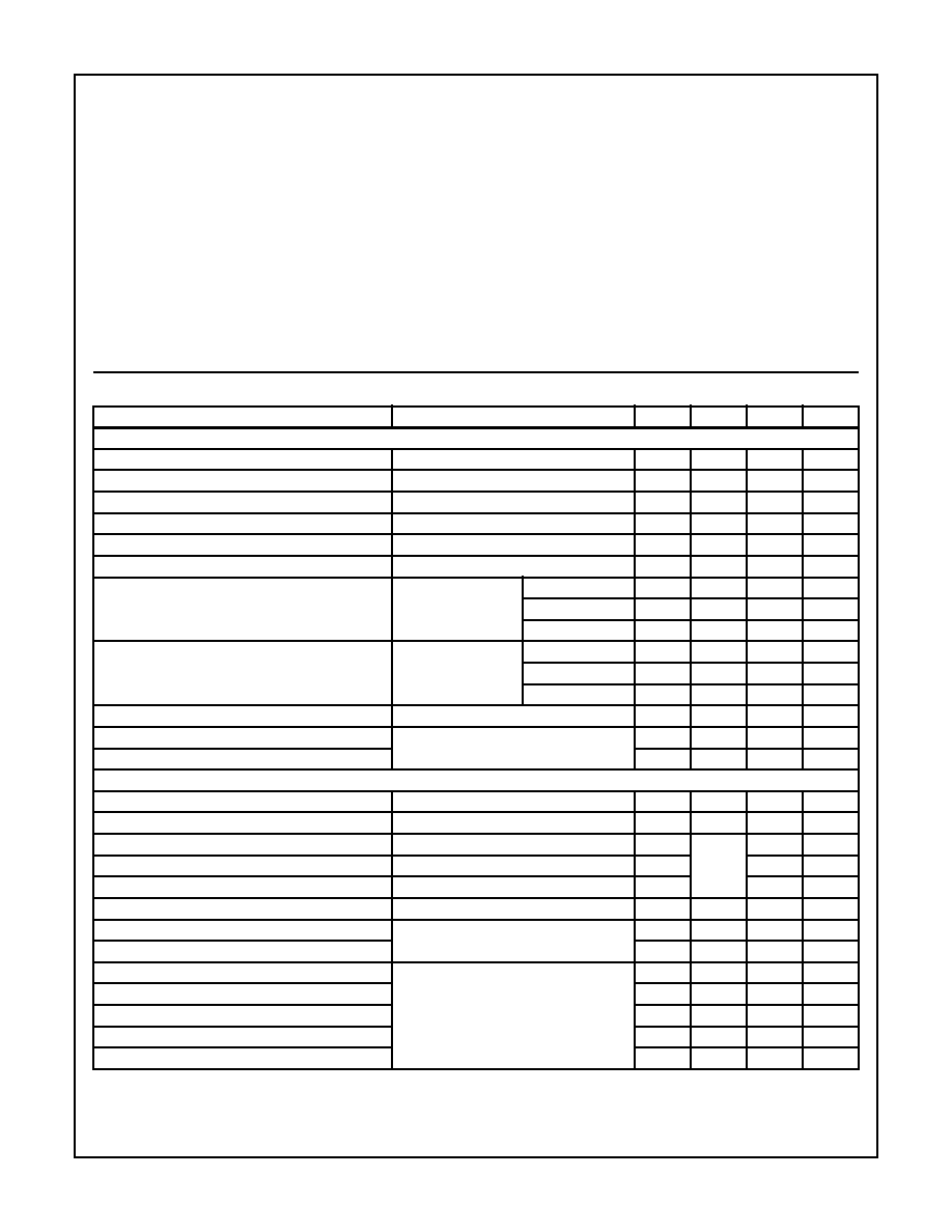
Electrical Specifications
T
A
= 25
o
C
PARAMETER
TEST CONDITIONS
MIN
TYP
MAX
UNITS
DC CHARACTERISTICS (For Each Transistor)
Collector-to-Base Breakdown Voltage
I
C
= 10
�
A, I
E
= 0
20
32
-
V
Collector-to-Emitter Breakdown Voltage
I
C
= 1mA, I
B
= 0
15
24
-
V
Collector-to-Substrate Breakdown-Voltage
I
C1
= 10
�
A, I
B
= 0, I
E
= 0
20
60
-
V
Emitter-to-Base Breakdown Voltage (Note 3)
I
E
= 10
�
A, I
C
= 0
4
5.7
-
V
Collector-Cutoff-Current
V
CE
= 10V I
B
= 0
-
-
0.5
�
A
Collector-Cutoff-Current
V
CB
= 10V, I
E
= 0
-
-
40
nA
DC Forward-Current Transfer Ratio
V
CE
= 6V
I
C
= 5mA
35
88
-
I
C
= 1mA
40
90
-
I
C
= 0.1mA
35
85
-
Base-to-Emitter Voltage
V
CE
= 6V
I
C
= 5mA
0.71
0.81
0.91
V
I
C
= 1mA
0.66
0.76
0.86
V
I
C
= 0.1mA
0.60
0.70
0.80
V
Collector-to-Emitter Saturation Voltage
I
C
= 10mA, I
B
= 1mA
-
0.26
0.50
V
Magnitude of Difference in V
BE
Q
1
and Q
2
Matched
V
CE
= 6V, I
C
= 1mA
-
0.5
5
mV
Magnitude of Difference in I
B
-
0.2
3
�
A
DYNAMIC CHARACTERISTICS
Noise Figure
f = 100kHz, R
S
= 500
, I
C
= 1mA
-
2.2
-
dB
Gain-Bandwidth Product
V
CE
= 6V, I
C
= 5mA
-
1.15
-
GHz
Collector-to-Base Capacitance
V
CB
= 6V, f = 1MHz
-
See
Fig. 5
-
pF
Collector-to-Substrate Capacitance
V
CI
= 6V, f = 1MHz
-
-
pF
Emitter-to-Base Capacitance
V
BE
= 4V, f = 1MHz
-
-
pF
Voltage Gain
V
CE
= 6V, f = 10MHz, R
L
= 1k
, I
C
= 1mA
-
28
-
dB
Power Gain
Cascode Configuration
f = 100MHz, V+ = 12V, I
C
= 1mA
27
30
-
dB
Noise Figure
-
3.5
-
dB
Input Resistance
Common-Emitter Configuration
V
CE
= 6V, I
C
= 1mA, f = 200 MHz
-
400
-
Output Resistance
-
4.6
-
k
Input Capacitance
-
3.7
-
pF
Output Capacitance
-
2
-
pF
Magnitude of Forward Transadmittance
-
24
-
mS
NOTE:
3. When used as a zener for reference voltage, the device must not be subjected to more than 0.1mJ of energy from any possible capacitance
or electrostatic discharge in order to prevent degradation of the junction. Maximum operating zener current should be less than 10mA.
5-3
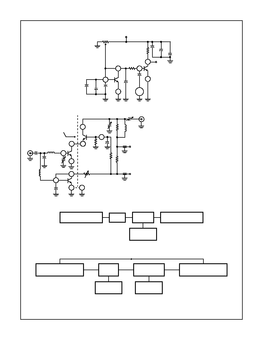
Test Circuits
FIGURE 1. VOLTAGE-GAIN TEST CIRCUIT USING CURRENT-MIRROR BIASING FOR Q
2
FIGURE 2. 100MHz POWER-GAIN AND NOISE-FIGURE TEST CIRCUIT
FIGURE 3A. POWER GAIN SET-UP
FIGURE 3B. NOISE FIGURE SET-UP
FIGURE 3. BLOCK DIAGRAMS OF POWER-GAIN AND NOISE-FIGURE TEST SET-UPS
7
8
4
2
3
6
GEN
10k
BIAS-CURRENT
ADJ
V+
R
L
470
0.01
1
�
F
V
O
Q
2
0.01
�
F
470pF
51
V
I
Q
3
0.01
1
�
F
pF
�
F
�
F
470pF
1000
pF
NOTES:
4. This circuit was chosen because it conveniently repre-
sents a close approximation in performance to a proper-
ly unilateralized single transistor of this type. The use of
Q
3
in a current-mirror configuration facilitates simplified
biasing. The use of the cascode circuit in no way implies
that the transistors cannot be used individually.
5. E.F. Johnson number 160-104-1 or equivalent.
4
3
2
13
12
14
6
7
5
8
SHIELD
Q
5
620
Q
2
C
1
1.8pF
0.3
�
H
1000pF
V
I
OHMITE
Z144
(NOTE 5)
Q
3
25k
1000
pF
1000
pF
560
750
1%
1000
pF
8.2
k
0.47
�
H
1.5 - 8pF
V
O
+12V
C
2
TEST
POINT
(NOTE 5)
ATTN
100MHz
BOONTON 91C
RF VOLTMETER
12V
DC
POWER SUPPLY
TEST SET
GENERAL RADIO 1021-P1
100MHz GENERATOR
100MHz
100MHz
NOISE FIGURE METER
POST AMPLIFIER
VHF NOISE SOURCE
HEWLETT PACKARD HP343A
TEST SET
HEWLETT PACKARD HP342A
12V
DC
POWER SUPPLY
15V
DC
POWER SUPPLY
CA3127
5-4
CA3127
Typical Performance Curves
FIGURE 4. NOISE FIGURE vs COLLECTOR CURRENT
FIGURE 5. NOISE FIGURE vs COLLECTOR CURRENT
FIGURE 6. GAIN-BANDWIDTH PRODUCT vs COLLECTOR
CURRENT
FIGURE 7. BASE-TO-EMITTER VOLTAGE vs COLLECTOR
CURRENT
FIGURE 8A. CAPACITANCE vs BIAS VOLTAGE FOR Q
2
FIGURE 8B. TYPICAL CAPACITANCE VALUES AT f = 1MHz.
THREE TERMINAL MEASUREMENT. GUARD ALL
TERMINALS EXCEPT THOSE UNDER TEST.
30
20
10
0
NOISE FIGURE (dB)
0.01
0.1
1.0
COLLECTOR CURRENT (mA)
T
A
= 25
o
C
R
SOURCE
= 500
f = 10Hz
f = 100Hz
f = 1kHz
f = 10kHz
f = 100kHz
V
CE
= 6V
30
20
10
0
NOISE FIGURE (dB)
0.01
0.1
1.0
COLLECTOR CURRENT (mA)
f = 10Hz
f = 100Hz
f = 1kHz
f = 10kHz
f = 100kHz
T
A
= 25
o
C
R
SOURCE
= 1k
V
CE
= 6V
T
A
= 25
o
C
V
CE
= 6V
GAIN-B
AND
WIDTH PR
ODUCT (GHz)
1.2
1.1
1.0
0.9
0.8
1
2
3
4
5
6
7
8
9
10
COLLECTOR CURRENT (mA)
0
B
ASE-T
O-EMITTER V
O
L
T
A
GE (V)
1.0
0.9
0.8
0.7
0.6
0.5
0.4
0.1
COLLECTOR CURRENT (mA)
1
10
T
A
= 25
o
C
T
A
= -55
o
C
T
A
= 125
o
C
CAP
A
CIT
ANCE (pF)
BIAS VOLTAGE (V)
2.25
1.25
1.00
0.75
0.50
0.25
0
1
2
3
4
5
6
7
8
9
10
C
CB
C
CI
C
EB
T
A
= 25
o
C
f = 1MHz
1.50
1.75
2.00
TRAN-
SISTOR
CAPACITANCE (pF)
C
CB
C
CE
C
EB
C
CI
PKG TOTAL PKG TOTAL PKG TOTAL PKG TOTAL
BIAS
(V)
-
6V
-
6V
-
4V
-
6V
Q
1
0.025 0.190 0.090 0.125 0.365 0.610 0.475
1.65
Q
2
0.015 0.170 0.225 0.265 0.130 0.360 0.085
1.35
Q
3
0.040 0.200 0.215 0.240 0.360 0.625 0.210
1.40
Q
4
0.040 0.190 0.225 0.270 0.365 0.610 0.085
1.25
Q
5
0.010 0.165 0.095 0.115 0.140 0.365 0.090
1.35
CA3127

5-5
CA3127
FIGURE 9. VOLTAGE GAIN vs FREQUENCY
FIGURE 10. VOLTAGE GAIN vs FREQUENCY
FIGURE 11. DC FORWARD-CURRENT TRANSFER RATIO (h
FE
)
vs COLLECTOR CURRENT
FIGURE 12. INPUT ADMITTANCE (Y
11
) vs FREQUENCY
FIGURE 13. INPUT ADMITTANCE (Y
11
) vs COLLECTOR
CURRENT
FIGURE 14. OUTPUT ADMITTANCE (Y
22
) vs FREQUENCY
Typical Performance Curves
(Continued)
T
A
= 25
o
C, V
CE
= 6V, R
L
= 100
FOR TEST CIRCUIT SEE FIGURE 19
V
O
L
T
A
GE GAIN (dB)
FREQUENCY (MHz)
I
C
= 0.2mA
I
C
= 0.5mA
I
C
= 1mA
I
C
= 5mA
40
35
30
25
20
15
10
5
0
-5
-10
1
10
100
1000
V
O
L
T
A
GE GAIN (dB)
FREQUENCY (MHz)
I
C
= 0.2mA
I
C
= 0.5mA
I
C
= 1mA
I
C
= 5mA
40
35
30
25
20
15
10
5
0
-5
-10
1
10
100
1000
T
A
= 25
o
C, V
CE
= 6V, R
L
= 1k
FOR TEST CIRCUIT SEE FIGURE 19
DC FOR
W
ARD CURRENT TRANSFER RA
TIO
100
90
80
70
60
50
0.1
1.0
10
COLLECTOR CURRENT (mA)
40
T
A
= 25
o
C
V
CE
= 6V
INPUT CONDUCT
ANCE (g
11
) OR
SUSCEPT
ANCE (b
11
) (mS)
FREQUENCY (MHz)
b
11
g
11
8
7
6
5
4
3
2
1
0
100
1000
T
A
= 25
o
C, V
CE
= 6V, I
C
= 1mA
INPUT CONDUCT
ANCE (g
11
) OR
SUSCEPT
ANCE (b
11
) (mS)
b
11
g
11
8
7
6
5
4
3
2
1
0
1
10
0
2
3
4
5
6
7
8
9
T
A
= 25
o
C
V
CE
= 6V
f = 200MHz
9
COLLECTOR CURRENT (mA)
OUTPUT CONDUCT
ANCE (g
22
) (mS)
OUTPUT SUSCEPT
ANCE (b
22
) (mS)
T
A
= 25
o
C
V
CE
= 6V
I
C
= 1mA
1.3
1.2
1.1
1.0
0.9
0.8
0.7
0.6
0.5
0.4
0.3
0.2
0.1
0
100
8
7
6
5
4
3
2
1
0
1000
FREQUENCY (MHz)
b
22
g
22