 | –≠–ª–µ–∫—Ç—Ä–æ–Ω–Ω—ã–π –∫–æ–º–ø–æ–Ω–µ–Ω—Ç: CA3160E | –°–∫–∞—á–∞—Ç—å:  PDF PDF  ZIP ZIP |
1
CA3160, CA3160A
4MHz, BiMOS Operational Amplifier with
MOSFET Input/CMOS Output
The CA3160A and CA3160 are integrated circuit operational
amplifiers that combine the advantage of both CMOS and
bipolar transistors on a monolithic chip. The CA3160 series are
frequency compensated versions of the popular CA3130
series.
Gate protected P-Channel MOSFET (PMOS) transistors are
used in the input circuit to provide very high input
impedance, very low input current, and exceptional speed
performance. The use of PMOS field effect transistors in the
input stage results in common-mode input voltage capability
down to 0.5V below the negative supply terminal, an
important attribute in single supply applications.
A complementary symmetry MOS (CMOS) transistor-pair,
capable of swinging the output voltage to within 10mV of
either supply voltage terminal (at very high values of load
impedance), is employed as the output circuit.
The CA3160 Series circuits operate at supply voltages
ranging from 5V to 16V, or
±
2.5V to
±
8V when using split
supplies, and have terminals for adjustment of offset voltage
for applications requiring offset null capability. Terminal
provisions are also made to permit strobing of the output
stage.
The CA3160A offers superior input characteristics over
those of the CA3160.
Features
∑ MOSFET Input Stage Provides:
- Very High Z
I
= 1.5T
(1.5 x 10
12
) (Typ)
- Very Low I
I
. . . . . . . . . . . . . 5pA (Typ) at 15V Operation
. . . . . . . . . . . . . . . . . . . . . . . 2pA (Typ) at 5V Operation
∑ Common-Mode Input Voltage Range Includes
Negative Supply Rail; Input Terminals Can Be Swung
0.5V Below Negative Supply Rail
∑ CMOS Output Stage Permits Signal Swing to Either (or
Both) Supply Rails
Applications
∑ Ground Referenced Single Supply Amplifiers
∑ Fast Sample Hold Amplifiers
∑ Long Duration Timers/Monostables
∑ High Input Impedance Wideband Amplifiers
∑ Voltage Followers (e.g., Follower for Single Supply
D/A Converter)
∑ Wien-Bridge Oscillators
∑ Voltage Controlled Oscillators
∑ Photo Diode Sensor Amplifiers
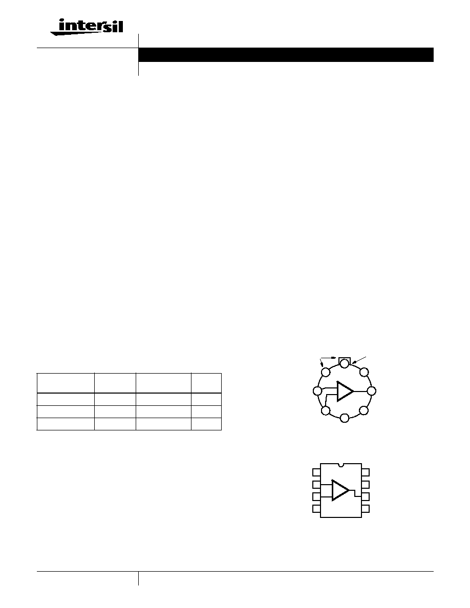
Pinouts
CA3160
(METAL CAN)
TOP VIEW
CA3160
(PDIP)
TOP VIEW
NOTE: CA3160 Series devices have an on-chip frequency
compensation network. Supplementary phase compensation or
frequency roll-off (if desired) can be connected externally between
Terminals 1 and 8.
Ordering Information
PART NUMBER
TEMP.
RANGE (
o
C)
PACKAGE
PKG.
NO.
CA3160AE
-55 to 125
8 Ld PDIP
E8.3
CA3160E
-55 to 125
8 Ld PDIP
E8.3
CA3160T
-55 to 125
8 Pin Metal Can
T8.C
TAB
OUTPUT
INV.
V- AND CASE
OFFSET
NON-INV.
V+
OFFSET
2
4
6
1
3
7
5
8
-
+
NULL
INPUT
INPUT
NULL
STROBE
SUPPLEMENTARY
COMPENSATION
OFFSET NULL
INV.
NON-INV.
V-
1
2
3
4
8
7
6
5
STROBE
V+
OUTPUT
OFFSET NULL
-
+
INPUT
INPUT
Data Sheet
September 1998
File Number
976.3
CAUTION: These devices are sensitive to electrostatic discharge; follow proper IC Handling Procedures.
1-888-INTERSIL or 321-724-7143
|
Copyright
©
Intersil Corporation 1999
2
Absolute Maximum Ratings
Thermal Information
Supply Voltage (Between V+ and V- Terminals) . . . . . . . . . . . +16V
Differential Mode Input Voltage . . . . . . . . . . . . . . . . . . . . . . . . . . .8V
Input Voltage . . . . . . . . . . . . . . . . . . . . . . . . . (V+ +8V) to (V- -0.5V)
Input Current . . . . . . . . . . . . . . . . . . . . . . . . . . . . . . . . . . . . . . . 1mA
Output Short Circuit Duration (Note 2). . . . . . . . . . . . . . . . Indefinite
Operating Conditions
Temperature Range . . . . . . . . . . . . . . . . . . . . . . . . . -55
o
C to 125
o
C
Thermal Resistance (Typical, Note 1)
JA
(
o
C/W)
JC
(
o
C/W)
PDIP Package . . . . . . . . . . . . . . . . . . .
110
N/A
Metal Can Package . . . . . . . . . . . . . . .
170
85
Maximum Junction Temperature (Metal Can) . . . . . . . . . . . . . . .175
o
C
Maximum Junction Temperature (Plastic Package) . . . . . . . .150
o
C
Maximum Storage Temperature Range . . . . . . . . . . -65
o
C to 150
o
C
Maximum Lead Temperature (Soldering 10s) . . . . . . . . . . . . 300
o
C
CAUTION: Stresses above those listed in "Absolute Maximum Ratings" may cause permanent damage to the device. This is a stress only rating and operation of the
device at these or any other conditions above those indicated in the operational sections of this specification is not implied.
NOTES:
1.
JA
is measured with the component mounted on an evaluation PC board in free air.
2. Short Circuit may be applied to ground or to either supply.
Electrical Specifications
T
A
= 25
o
C, V+ = 15V, V- = 0V, Unless Otherwise Specified
PARAMETER
SYMBOL
TEST CONDITIONS
CA3160
CA3160A
UNITS
MIN
TYP
MAX
MIN
TYP
MAX
Input Offset Voltage
|V
IO
|
V
S
=
±
7.5V
-
6
15
-
2
5
mV
Input Offset Current
|I
IO
|
V
S
=
±
7.5V
-
0.5
30
-
0.5
20
pA
Input Current
I
I
V
S
=
±
7.5V
-
5
50
-
5
30
pA
Large-Signal Voltage Gain
A
OL
V
O
= 10V
P-P
, R
L
= 2k
50
320
-
50
320
-
kV/V
94
110
-
94
110
-
dB
Common-Mode Rejection Ratio
CMRR
70
90
-
80
95
-
dB
Common-Mode Input-Voltage Range
V
lCR
0
-0.5 to 12
10
0
-0.5 to 12
10
V
Power-Supply Rejection Ratio
PSRR
V
IO
/
V
S
, V
S
=
±
7.5V
-
32
320
-
32
150
µ
V/V
Maximum Output Voltage
V
OM
+
R
L
= 2k
12
13.3
-
12
13.3
-
V
V
OM
-
-
0.002
0.01
-
0.002
0.01
V
V
OM
+
R
L
=
14.99
15
-
14.99
15
-
V
V
OM
-
-
0
0.01
-
0
0.01
V
Maximum Output Current
I
OM
+
V
O
= 0V (Source)
12
22
45
12
22
45
mA
I
OM
-
V
O
= 15V (Sink)
12
20
45
12
20
45
mA
Supply Current (Note 3)
I+
V
O
= 7.5V, R
L
=
-
10
15
-
10
15
mA
V
O
= 0V, R
L
=
-
2
3
-
2
3
mA
Input Offset Voltage Temperature Drift
V
IO
/
T
-
8
-
-
6
-
µ
V/
o
C
Electrical Specifications
For Design Guidance, V
SUPPLY
=
±
7.5V, T
A
= 25
o
C, Unless Otherwise Specified
PARAMETER
SYMBOL
TEST CONDITIONS
CA3160
CA3160A
UNITS
TYP
TYP
Input Offset Voltage Adjustment Range
10k
Across Terminals 4 and 5 or
Terminals 4 and 1
±
22
±
22
mV
Input Resistance
R
I
1.5
1.5
T
Input Capacitance
C
I
f = 1MHz
4.3
4.3
pF
Equivalent Input Noise Voltage
e
N
BW = 0.2MHz
R
S
= 1M
40
40
µ
V
R
S
= 10M
50
50
µ
V
Equivalent Input Noise Voltage
e
N
R
S
= 100
1kHz
72
72
nV/
Hz
10kHz
30
30
nV/
Hz
CA3160, CA3160A
3
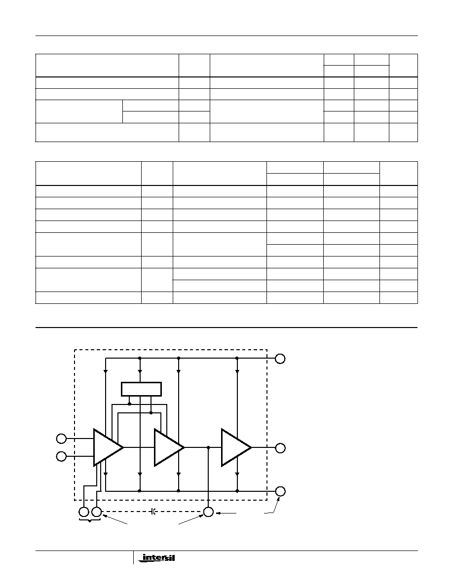
Block Diagram
Unity Gain Crossover Frequency
f
T
4
4
MHz
Slew Rate
SR
10
10
V/
µ
s
Transient Response
Rise and Fall Time
t
r
C
L
= 25pF, R
L
= 2k
, (Voltage Follower)
0.09
0.09
µ
s
Overshoot
OS
10
10
%
Settling Time
t
S
C
L
= 25pF, R
L
= 2k
, (Voltage Follower)
To <0.1%, V
IN
= 4V
P-P
1.8
1.8
µ
s
Electrical Specifications
For Design Guidance, V
SUPPLY
=
±
7.5V, T
A
= 25
o
C, Unless Otherwise Specified (Continued)
PARAMETER
SYMBOL
TEST CONDITIONS
CA3160
CA3160A
UNITS
TYP
TYP
Electrical Specifications
For Design Guidance, V+ = +5V, V- = 0V, T
A
= 25
o
C, Unless Otherwise Specified
PARAMETER
SYMBOL
TEST CONDITIONS
CA3160
CA3160A
UNITS
TYP
TYP
Input Offset Voltage
V
IO
6
2
mV
Input Offset Current
I
IO
0.1
0.1
pA
Input Current
I
l
2
2
pA
Common-Mode Rejection Ratio
CMRR
80
90
dB
Large Signal Voltage Gain
A
OL
V
O
= 4V
P-P
, R
L
= 5k
100
100
kV/V
100
100
dB
Common-Mode Input Voltage Range
V
lCR
0 to 2.8
0 to 2.8
V
Supply Current
I+
V
O
= 5V, R
L
=
300
300
µ
A
V
O
= 2.5V, R
L
=
500
500
µ
A
Power Supply Rejection Ratio
PSRR
V
IO
/
V+
200
200
µ
V/V
NOTE:
3. I
CC
typically increases by 1.5mA/MHz during operation.
6
BIAS CKT.
200
µ
A
1.35mA
200
µ
A
7
8mA
(NOTE 4)
OUTPUT
A
V
30X
A
V
6000X
STROBE
V-
V+
OFFSET
NULL
COMPENSATION
(WHEN DESIRED)
+
-
INPUT
A
V
5X
C
C
NOTES:
4. Total supply voltage (for indicated voltage
gains) = 15V with input terminals biased so
that Terminal 6 potential is +7.5V above
Terminal 4.
5. Total supply voltage (for indicated voltage
gains) = 15V with output terminal driven to
either supply rail.
0mA
(NOTE 5)
4
8
1
5
2
3
CA3160, CA3160A
4
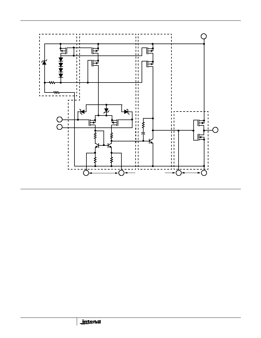
Schematic Diagram
Application Information
Circuit Description
Refer to the Block Diagram of the CA3160 series CMOS
Operational Amplifiers. The input terminals may be operated
down to 0.5V below the negative supply rail, and the output
can be swung very close to either supply rail in many
applications. Consequently, the CA3160 series circuits are
ideal for single supply operation. Three class A amplifier
stages, having the individual gain capability and current
consumption shown in the Block Diagram provide the total
gain of the CA3160. A biasing circuit provides two potentials
for common use in the first and second stages. Terminals 8
and 1 can be used to supplement the internal phase
compensation network if additional phase compensation or
frequency roll-off is desired. Terminals 8 and 4 can also be
used to strobe the output stage into a low quiescent current
state. When Terminal 8 is tied to the negative supply rail
(Terminal 4) by mechanical or electrical means, the output
potential at Terminal 6 essentially rises to the positive supply-
rail potential at Terminal 7. This condition of essentially zero
current drain in the output stage under the strobed "OFF"
condition can only be achieved when the ohmic load
resistance presented to the amplifier is very high (e.g., when
the amplifier output is used to drive MOS digital circuits in
comparator applications).
Input Stage - The circuit of the CA3160 is shown in the
Schematic Diagram. It consists of a differential-input stage
using PMOS field-effect transistors (Q
6
, Q
7
) working into a
mirror-pair of bipolar transistors (Q
9
, Q
10
) functioning as load
resistors together with resistors R
3
through R
6
. The mirror-
pair transistors also function as a differential-to-single-ended
converter to provide base drive to the second-stage bipolar
transistor (Q
11
). Offset nulling, when desired, can be effected
by connecting a 100,000
potentiometer across Terminals 1
and 5 and the potentiometer slider arm to Terminal 4.
Cascode-connected PMOS transistors Q
2
, Q
4
, are the
constant-current source for the input stage. The biasing circuit
for the constant-current source is subsequently described.
The small diodes D
5
through D
7
provide gate-oxide protection
against high-voltage transients, including static electricity
during handling for Q
6
and Q
7
.
Second-Stage - Most of the voltage gain in the CA3160 is
provided by the second amplifier stage, consisting of bipolar
7
4
8
1
5
2
3
BIAS CURRENT
"CURRENT SOURCE
LOAD" FOR Q
11
Q
2
D
1
D
2
D
3
D
4
Z
1
8.3V
Q
1
R
1
40k
Q
4
R
2
5k
INPUT STAGE
D
5
NON-INV.
INPUT
INV. INPUT
+
-
Q
6
R
3
1k
Q
9
Q
10
R
5
1k
R
6
1k
R
4
1k
Q
7
D
6
D
7
Q
3
OFFSET NULL
Q
11
SUPPLEMENTARY
COMP IF DESIRED
STROBING
SECOND
OUTPUT
Q
8
Q
12
STAGE
STAGE
Q
5
V+
2k
30
pF
6
OUTPUT
NOTE: Diodes D
5
Through D
7
Provide Gate Oxide Protection For MOSFET Input Stage.
CURRENT SOURCE
FOR Q
6
AND Q
7
CA3160, CA3160A

5
transistor Q
11
and its cascode-connected load resistance
provided by PMOS transistors Q
3
and Q
5
. The source of bias
potentials for these PMOS transistors is described later. Miller
Effect compensation (roll off) is accomplished by means of the
30pF capacitor and 2k
resistor connected between the base
and collector of transistor Q
11
. These internal components
provide sufficient compensation for unity gain operation in
most applications. However, additional compensation, if
desired, may be used between Terminals 1 and 8.
Bias-Source Circuit - At total supply voltages, somewhat
above 8.3V, resistor R
2
and zener diode Z
1
serve to establish a
voltage of 8.3V across the series-connected circuit, consisting
of resistor R
1
, diodes D
1
through D
4
, and PMOS transistor Q
1
.
A tap at the junction of resistor R
1
and diode D
4
provides a
gate-bias potential of about 4.5V for PMOS transistors Q
4
and
Q
5
with respect to Terminal 7. A potential of about 2.2V is
developed across diode-connected PMOS transistor Q
1
with
respect to Terminal 7 to provide gate bias for PMOS transistors
Q
2
and Q
3
. It should be noted that Q
1
is "mirror-connected" to
both Q
2
and Q
3
. Since transistors Q
1
, Q
2
, Q
3
are designed to
be identical, the approximately 200
µ
A current in Q
1
establishes
a similar current in Q
2
and Q
3
as constant-current sources for
both the first and second amplifier stages, respectively.
At total supply voltages somewhat less than 8.3V, zener diode
Z
1
becomes nonconductive and the potential, developed
across series-connected R
1
, D
1
- D
4
, and Q
1
, varies directly
with variations in supply voltage. Consequently, the gate bias
for Q
4
, Q
5
and Q
2
, Q
3
varies in accordance with supply-
voltage variations. This variation results in deterioration of the
power-supply-rejection ratio (PSRR) at total supply voltages
below 8.3V. Operation at total supply voltages below about
4.5V results in seriously degraded performance.
Output Stage - The output stage consists of a drain-loaded
inverting amplifier using CMOS transistors operating in the
Class A mode. When operating into very high resistance loads,
the output can be swung within millivolts of either supply rail.
Because the output stage is a drain-loaded amplifier, its gain is
dependent upon the load impedance. The transfer
characteristics of the output stage for a load returned to the
negative supply rail are shown in Figure 17. Typical op amp
loads are readily driven by the output stage. Because large-
signal excursions are non-linear, requiring feedback for good
waveform reproduction, transient delays may be encountered.
As a voltage follower, the amplifier can achieve 0.01% accuracy
levels, including the negative supply rail.
Offset Nulling
Offset-voltage nulling is usually accomplished with a
100,000
potentiometer connected across Terminals 1 and
5 and with the potentiometer slider arm connected to
Terminal 4. A fine offset-null adjustment usually can be
effected with the slider arm positioned in the mid-point of the
potentiometer's total range.
Input Current Variation with Common Mode Input
Voltage
As shown in the Electrical Specifications, the input current for
the CA3160 Series Op Amps is typically 5pA at T
A
= 25
o
C
when Terminals 2 and 3 are at a common-mode potential of
+7.5V with respect to negative supply Terminal 4. Figure 23
contains data showing the variation of input current as a
function of common-mode input voltage at T
A
= 25
o
C. These
data show that circuit designers can advantageously exploit
these characteristics to design circuits which typically require
an input current of less than 1pA, provided the common-mode
input voltage does not exceed 2V. As previously noted, the
input current is essentially the result of the leakage current
through the gate-protection diodes in the input circuit and,
therefore, a function of the applied voltage. Although the finite
resistance of the glass terminal-to-case insulator of the metal
can package also contributes an increment of leakage current,
there are useful compensating factors. Because the gate-
protection network functions as if it is connected to Terminal 4
potential, and the metal can case of the CA3160 is also
internally tied to Terminal 4, input Terminal 3 is essentially
"guarded" from spurious leakage currents.
Input-Current Variation with Temperature
The input current of the CA3160 Series circuits is typically 5pA
at 25
o
C. The major portion of this input current is due to
leakage current through the gate-protective diodes in the input
circuit. As with any semiconductor junction device, including op
amps with a junction-FET input stage, the leakage current
approximately doubles for every 10
o
C increase in temperature.
Figure 24 provides data on the typical variation of input bias
current as a function of temperature in the CA3160.
In applications requiring the lowest practical input current and
incremental increases in current because of "warm-up" effects,
it is suggested that an appropriate heat sink be used with the
CA3160. In addition, when "sinking" or "sourcing" significant
output current the chip temperature increases, causing an
increase in the input current. In such cases, heat-sinking can
also very markedly reduce and stabilize input current variations.
Input Offset Voltage (V
IO
) Variation with DC Bias
vs Device Operating Life
It is well known that the characteristics of a MOSFET device
can change slightly when a DC gate-source bias potential is
applied to the device for extended time periods. The magnitude
of the change is increased at high temperatures. Users of the
CA3160 should be alert to the possible impacts of this effect if
the application of the device involves extended operation at
high temperatures with a significant differential DC bias voltage
applied across Terminals 2 and 3. Figure 25 shows typical data
pertinent to shifts in offset voltage encountered with CA3160
devices in metal can packages during life testing. At lower
temperatures (metal can and plastic) for example at 85
o
C, this
change in voltage is considerably less. In typical linear
applications where the differential voltage is small and
symmetrical, these incremental changes are of about the same
CA3160, CA3160A