 | –≠–ª–µ–∫—Ç—Ä–æ–Ω–Ω—ã–π –∫–æ–º–ø–æ–Ω–µ–Ω—Ç: CA3183AE | –°–∫–∞—á–∞—Ç—å:  PDF PDF  ZIP ZIP |
1
TM
File Number
532.5
CAUTION: These devices are sensitive to electrostatic discharge; follow proper IC Handling Procedures.
1-888-INTERSIL or 321-724-7143
|
Intersil and Design is a trademark of Intersil Corporation.
|
Copyright
©
Intersil Corporation 2000
CA3146, CA3146A, CA3183, CA3183A
High-Voltage Transistor Arrays
The CA3146A, CA3146, CA3183A, and CA3183 are general
purpose high voltage silicon NPN transistor arrays on a
common monolithic substrate.
Types CA3146A and CA3146 consist of five transistors with two
of the transistors connected to form a differentially connected
pair. These types are recommended for low power applications
in the DC through VHF range. (CA3146A and CA3146 are high
voltage versions of the popular predecessor type CA3046.)
Types CA3183A and CA3183 consist of five high current
transistors with independent connections for each transistor.
In addition two of these transistors (Q
1
and Q
2
) are matched
at low current (i.e., 1mA) for applications where offset
parameters are of special importance. A special substrate
terminal is also included for greater flexibility in circuit
design. (CA3183A and CA3183 are high voltage versions of
the popular predecessor type CA3083.)
The types with an "A" suffix are premium versions of their
non-"A" counterparts and feature tighter control of
breakdown voltages making them more suitable for higher
voltage applications.
For detailed application information, see companion
Application Note AN5296 "Application of the CA3018
Integrated Circuit Transistor Array."
Features
∑ Matched General Purpose Transistors
- V
BE
Match . . . . . . . . . . . . . . . . . . . . . . . .
±
5mV (Max)
∑ Operation from DC to 120MHz (CA3146, CA3146A)
∑ Low Noise Figure . . . . . . . . . . 3.2dB (CA3146, CA3146A)
∑ High I
C
. . . . . . . . . . . . 75mA (Max) (CA3183, CA3183A)
Applications
∑ General Use in Signal Processing Systems in DC through
VHF Range
∑ Custom Designed Differential Amplifiers
∑ Temperature Compensated Amplifiers
∑ Lamp and Relay Drivers (CA3183, CA3183A)
∑ Thyristor Firing (CA3183, CA3183A)
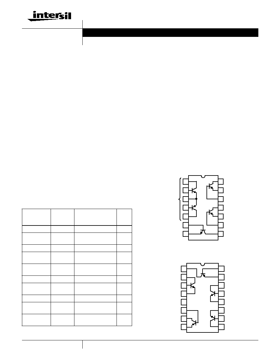
Pinouts
CA3146, CA3146A (PDIP, SOIC)
TOP VIEW
CA3183, CA3183A (PDIP, SOIC)
TOP VIEW
Ordering Information
PART
NUMBER
(BRAND)
TEMP.
RANGE
(
o
C)
PACKAGE
PKG.
NO.
CA3146AE
-40 to 85
14 Ld PDIP
E14.3
CA3146AM
(3146A)
-40 to 85
14 Ld SOIC
M14.15
CA3146E
-40 to 85
14 Ld PDIP
E14.3
CA3146M
(3146)
-40 to 85
14 Ld SOIC
M14.15
CA3146M96
(3146)
-40 to 85
14 Ld SOIC Tape and
Reel
M14.15
CA3183AE
-40 to 85
16 Ld PDIP
E16.3
CA3183AM96
(3183A)
-40 to 85
16 Ld SOIC Tape and
Reel
M16.15
CA3183E
-40 to 85
16 Ld PDIP
E16.3
CA3183M
(3183)
-40 to 85
16 Ld SOIC
M16.15
CA3183M96
(3183)
-40 to 85
16 Ld SOIC Tape and
Reel
M16.15
SUBSTRATE
1
2
3
4
5
6
7
14
13
12
11
10
9
8
Q
1
Q
2
Q
4
Q
3
DIFF.
PAIR
Q
5
14
15
16
9
13
12
11
10
1
2
3
4
5
7
6
8
SUBSTRATE
Q
1
Q
3
Q
2
Q
4
Q
5
Data Sheet
April 2000
[ /Title
(CA31
46,
CA314
6A,
CA318
3,
CA318
3A)
/Sub-
ject
(High-
Volt-
age
Tran-
sistor
Arrays
)
/Autho
r ()
/Key-
words
(Inter-
sil
Corpo-
ration,
five,
transis-
tor
array,
low
cost
NPN,
40V,
50ma
75ma,
mhz ft,
high
volt-
2
Absolute Maximum Ratings
Thermal Information
Collector-to-Emitter Voltage (V
CEO
)
CA3146A, CA3183A . . . . . . . . . . . . . . . . . . . . . . . . . . . . . . . . . . 40V
CA3146, CA3183 . . . . . . . . . . . . . . . . . . . . . . . . . . . . . . . . . . . . 30V
Collector-to-Base Voltage (V
CBO
)
CA3146A, CA3183A . . . . . . . . . . . . . . . . . . . . . . . . . . . . . . . . . . 50V
CA3146, CA3183 . . . . . . . . . . . . . . . . . . . . . . . . . . . . . . . . . . . . 40V
Collector-to-Substrate Voltage (V
CIO
, Note 1)
CA3146A, CA3183A . . . . . . . . . . . . . . . . . . . . . . . . . . . . . . . . . . 50V
CA3146, CA3183 . . . . . . . . . . . . . . . . . . . . . . . . . . . . . . . . . . . . 40V
Emitter to Base Voltage (V
EBO
) all types. . . . . . . . . . . . . . . . . . . . . 5V
Collector Current
CA3146A, CA3146 . . . . . . . . . . . . . . . . . . . . . . . . . . . . . . . . . 50mA
CA3183A, CA3183 . . . . . . . . . . . . . . . . . . . . . . . . . . . . . . . . . 75mA
Base Current (I
B
) - CA3183A, CA3183 . . . . . . . . . . . . . . . . . . . 20mA
Operating Conditions
Temperature Range . . . . . . . . . . . . . . . . . . . . . . . . . . -40
o
C to 85
o
C
Thermal Resistance (Typical, Note 2)
JA
(
o
C/W)
14 Ld PDIP Package . . . . . . . . . . . . . . . . . . . . . . . .
100
14 Ld SOIC Package . . . . . . . . . . . . . . . . . . . . . . . .
200
16 Ld PDIP Package . . . . . . . . . . . . . . . . . . . . . . . .
95
16 Ld SOIC Package . . . . . . . . . . . . . . . . . . . . . . . .
175
Maximum Power Dissipation (Any One Transistor, Note 3)
CA3146A, CA3146. . . . . . . . . . . . . . . . . . . . . . . . . . . . . . . . 300mW
CA3183A, CA3183. . . . . . . . . . . . . . . . . . . . . . . . . . . . . . . . 500mW
Maximum Junction Temperature (Die). . . . . . . . . . . . . . . . . . . . 175
o
C
Maximum Junction Temperature (Plastic Package) . . . . . . . . .150
o
C
Maximum Storage Temperature Range (all types) . -65
o
C to 150
o
C
Maximum Lead Temperature (Soldering 10s) . . . . . . . . . . . . .300
o
C
(SOIC - Lead Tips Only)
CAUTION: Stresses above those listed in "Absolute Maximum Ratings" may cause permanent damage to the device. This is a stress only rating and operation of the
device at these or any other conditions above those indicated in the operational sections of this specification is not implied.
NOTES:
1. The collector of each transistor is isolated from the substrate by an integral diode. The substrate must be connected to a voltage which is more
negative than any collector voltage in order to maintain isolation between transistors, and to provide for normal transistor action. To avoid
undesired coupling between transistors, the substrate terminal should be maintained at either DC or signal (AC) ground. A suitable bypass
capacitor can be used to establish a signal ground.
2.
JA
is measured with the component mounted on an evaluation PC board in free air.
3. Care must be taken to avoid exceeding the maximum junction temperature. Use the total power dissipation (all transistors) and thermal
resistances to calculate the junction temperature.
Electrical Specifications
CA3146 Series
PARAMETER
SYMBOL
TEST CONDITIONS
TYPICAL
PERF.
CURVE
FIG. NO.
CA3146
CA3146A
UNITS
T
A
= 25
o
C
MN
TYP
MAX
MIN
TYP
MAX
DC CHARACTERISTICS FOR EACH TRANSISTOR
Collector-to-Base
Breakdown Voltage
V
(BR)CBO
I
C
= 10
µ
A, I
E
= 0
-
40
72
-
50
72
-
V
Collector-to-Emitter
Breakdown Voltage
V
(BR)CEO
I
C
= 1mA, I
B
= 0
-
30
56
-
40
56
-
V
Collector-to-Substrate
Breakdown Voltage
V
(BR)CIO
I
CI
= 10
µ
A, I
B
= 0,
I
E
= 0
-
40
72
-
50
72
-
V
Emitter-to-Base Breakdown Voltage
V
(BR)EBO
I
E
= 10
µ
A, I
C
= 0
-
5
7
-
5
7
-
V
Collector-Cutoff Current
I
CEO
V
CE
= 10V, I
B
= 0
1
-
See
Curve
5
-
See
Curve
5
µ
A
Collector-Cutoff Current
I
CBO
V
CB
= 10V, I
E
= 0
2
-
0.002
100
-
0.002
100
nA
DC Forward-Current Transfer
Ratio
h
FE
V
CE
= 5V, I
C
= 10mA
3
-
85
-
-
85
-
-
V
CE
= 5V, I
C
= 1mA
3
30
100
-
30
100
-
-
V
CE
= 5V, I
C
= 10
µ
A
3
-
90
-
-
90
-
-
Base-to-Emitter Voltage
V
BE
V
CE
= 3V, I
C
= 1mA
4
0.63
0.73
0.83
0.63
0.73
0.83
V
Collector-to-Emitter
Saturation Voltage
V
CE SAT
I
C
= 10mA, I
B
= 1mA
5
-
0.33
-
-
0.33
-
V
DC CHARACTERISTICS FOR TRANSISTORS Q
1
AND Q
2
(As A Differential Amplifier)
Magnitude of Input Offset
Voltage |V
BE1
- V
BE2
|
|V
IO
|
V
CE
= 5V, I
E
= 1mA
6, 7
-
0.48
5
-
0.48
5
mV
Magnitude of Base-to-Emitter
Temperature Coefficient
V
CE
= 5V, I
E
= 1mA
-
-
1.9
-
-
1.9
-
mV/
o
C
V
BE
T
----------------
CA3146, CA3146A, CA3183, CA3183A
3
Magnitude of V
IO
(V
BE1
- V
BE2
)
Temperature Coefficient
V
CE
= 5V,
I
C1
= I
C2
= 1mA
-
-
1.1
-
-
1.1
-
µ
V/
o
C
Magnitude of Input Offset Current
|I
IO1
- I
IO2
| (CA3146AE and
CA3146E Only)
I
IO
V
CE
= 5V,
I
C1
= I
C2
= 1mA
8
-
0.3
2
-
0.3
2
µ
A
DYNAMIC CHARACTERISTICS
Low Frequency Noise Figure
NF
f = 1kHz, V
CE
= 5V,
I
C
= 100
µ
A, Source
Resistance = 1k
10
-
3.25
-
-
3.25
-
dB
Low-Frequency, Small-Signal
Equivalent-Circuit Characteristics:
Forward-Current Transfer
Ratio
h
FE
f = 1kHz, V
CE
= 5V,
I
C
= 1mA
12
-
100
-
-
100
-
-
Short-Circuit Input Impedance
h
IE
f = 1kHz, V
CE
= 5V,
I
C
= 1mA
12
-
3.5
-
-
2.7
-
k
Open-Circuit Output Impedance
h
OE
f = 1kHz, V
CE
= 5V,
I
C
= 1mA
12
-
15.6
-
-
15.6
-
µ
S
Open-Circuit Reverse Voltage
Transfer Ratio
h
RE
f = 1kHz, V
CE
= 5V,
I
C
= 1mA
12
-
1.8 x
10
-4
-
-
1.8 x
10
-4
-
-
Admittance Characteristics:
Forward Transfer Admittance
Y
FE
f = 1MHz, V
CE
= 5V,
I
C
= 1 mA
13
-
31-
j1.5
-
-
31-j1.5
-
mS
Input Admittance
Y
IE
f = 1MHz, V
CE
= 5V,
I
C
= 1 mA
14
-
0.3 +
j0.04
-
-
0.35 +
j0.04
-
mS
Output Admittance
Y
OE
f = 1MHz, V
CE
= 5V,
I
C
= 1 mA
15
-
0.001
+ j0.03
-
-
0.001
+ j0.03
-
mS
Reverse Transfer
Admittance
Y
RE
f = 1MHz, V
CE
= 5V,
I
C
= 1 mA
16
See
Curve
See
Curve
mS
Gain-Bandwidth Product
f
T
V
CE
= 5V, I
C
= 3mA
17
300
500
-
300
500
-
MHz
Emitter-to-Base Capacitance
C
EB
V
EB
= 5V, I
E
= 0
18
-
0.70
-
-
0.70
-
pF
Collector-to-Base Capacitance
C
CB
V
CB
= 5V, I
C
= 0
18
-
0.37
-
-
0.37
-
pF
Collector-to-Substrate
Capacitance
C
Cl
V
Cl
= 5V, I
C
= 0
18
-
2.2
-
-
2.2
-
pF
Electrical Specifications
CA3183 Series
PARAMETER
SYMBOL
TEST CONDITIONS
TYPICAL
PERF.
CURVE
FIG. NO.
CA3183
CA3183A
UNITS
T
A
= 25
o
C
MIN
TYP
MAX
MIN
TYP
MAX
DC CHARACTERISTICS FOR EACH TRANSISTOR
Collector-to-Base
Breakdown Voltage
V
(BR)CBO
I
C
= 100
µ
A, I
E
= 0
-
40
-
-
50
-
-
V
Collector-to-Emitter
Breakdown Voltage
V
(BR)CEO
I
C
= 1mA, I
B
= 0
-
30
-
-
40
-
-
V
Collector-to-Substrate
Breakdown Voltage
V
(BR)ClO
I
CI
= 100
µ
A, I
B
= 0,
I
E
= 0
-
40
-
-
50
-
-
V
Emitter-to-Base
Breakdown Voltage
V
(BR)EBO
I
E
= 500
µ
A, I
C
= 0
-
5
-
-
5
-
-
V
Collector-Cutoff Current
I
CEO
V
CE
= 10V, I
B
= 0
19
-
-
10
-
-
10
µ
A
Electrical Specifications
CA3146 Series (Continued)
PARAMETER
SYMBOL
TEST CONDITIONS
TYPICAL
PERF.
CURVE
FIG. NO.
CA3146
CA3146A
UNITS
T
A
= 25
o
C
MN
TYP
MAX
MIN
TYP
MAX
V
IO
T
--------------
CA3146, CA3146A, CA3183, CA3183A
4
Collector-Cutoff Current
I
CBO
V
CB
= 10V, I
E
= 0
20
-
-
1
-
-
1
µ
A
DC Forward-Current
Transfer Ratio
h
FE
V
CE
= 3V, I
C
= 10mA
21, 22
40
-
-
40
-
-
-
V
CE
= 5V, I
C
= 50mA
-
40
-
-
40
-
-
-
Base-to-Emitter Voltage
V
BE
V
CE
= 3V, I
C
= 10mA
23
0.65
0.75
0.85
0.65
0.75
0.85
V
Collector-to-Emitter
Saturation Voltage
V
CE SAT
(Note 3)
I
C
= 50mA, I
B
= 5mA
24
-
1.7
3.0
-
1.7
3.0
V
FOR TRANSISTORS Q
1
AND Q
2
(AS A DIFFERENTIAL AMPLIFIER)
Absolute Input Offset
Voltage
|V
IO
|
V
CE
= 3V, I
C
= 1mA
25
-
0.47
5
-
0.47
5
mV
Absolute Input Offset
Current
|I
IO
|
V
CE
= 3V, I
C
= 1mA
26
-
0.78
2.5
-
0.78
2.5
µ
A
Electrical Specifications
CA3183 Series (Continued)
PARAMETER
SYMBOL
TEST CONDITIONS
TYPICAL
PERF.
CURVE
FIG. NO.
CA3183
CA3183A
UNITS
T
A
= 25
o
C
MIN
TYP
MAX
MIN
TYP
MAX
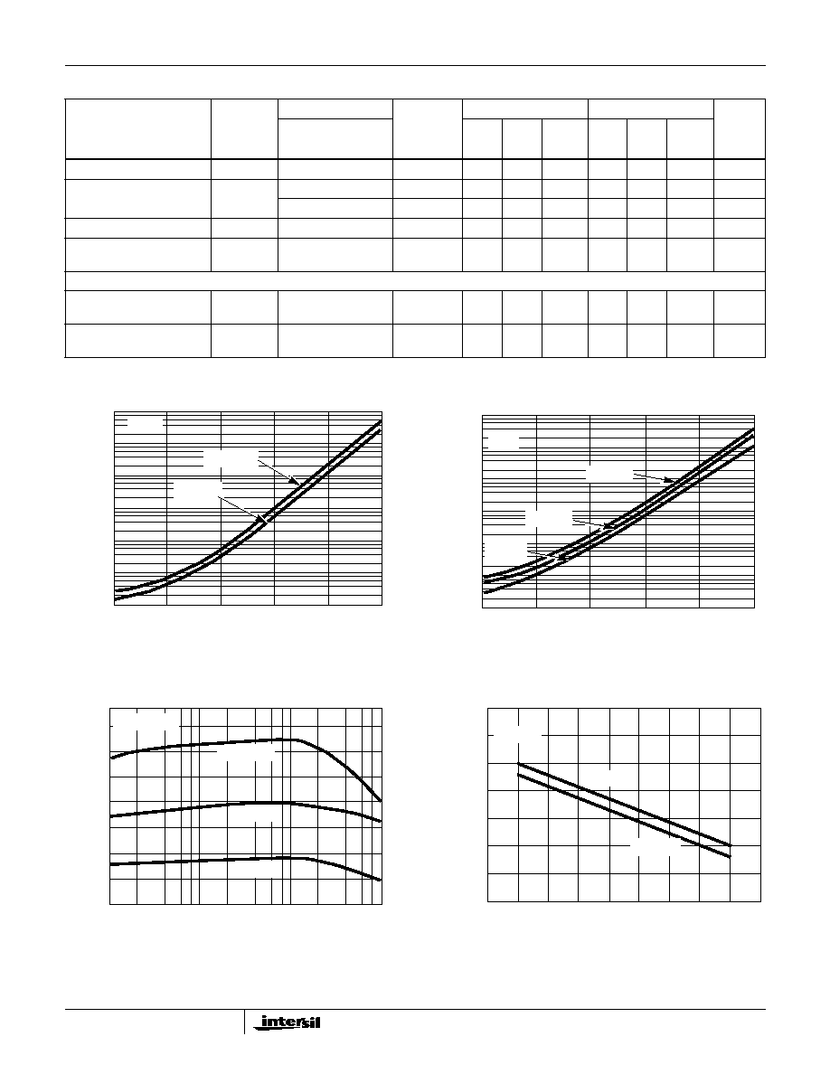
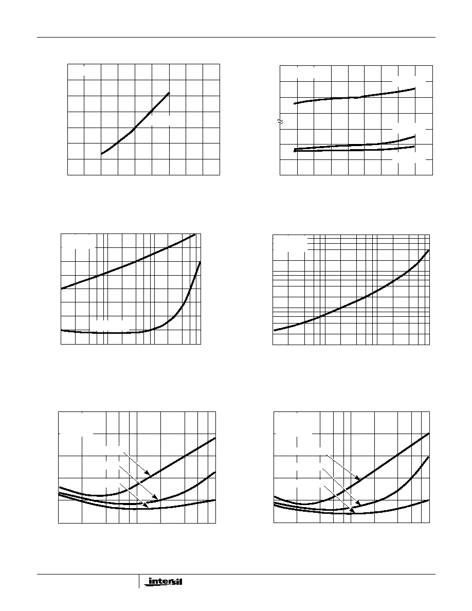
Typical Performance Curves
DC Characteristics - CA3146 Series
FIGURE 1. I
CEO
vs TEMPERATURE FOR ANY TRANSISTOR
FIGURE 2. I
CBO
vs TEMPERATURE FOR ANY TRANSISTOR
FIGURE 3. h
FE
vs I
C
FOR ANY TRANSISTOR
FIGURE 4. V
BE
vs TEMPERATURE FOR ANY TRANSISTOR
10
2
10
-1
10
1
10
-2
10
-3
COLLECT
OR CUT
OFF CURRENT (nA)
0
25
50
75
100
125
TEMPERATURE (
o
C)
I
B
= 0
V
CE
= 5V
10
3
V
CE
= 10V
COLLECT
OR CUT
OFF CURRENT (nA)
10
2
10
-4
10
1
10
-1
10
-2
10
-3
0
25
50
75
100
125
TEMPERATURE (
o
C)
I
E
= 0
V
CB
= 10
V
CB
= 5
V
CB
= 15
DC FOR
W
ARD CURRENT TRANSFER RA
TIO
140
120
100
80
60
40
0.01
1
10
COLLECTOR CURRENT (mA)
20
T
A
= 125
o
C
160
0.1
25
o
C
-55
o
C
V
CE
= 5V
I
E
= 3mA
I
E
= 1mA
TEMPERATURE (
o
C)
B
ASE T
O
EMITTER V
O
L
T
A
GE (V)
0.9
0.8
0.7
0.6
0.5
0.4
-75
V
CE
= 5V
-50
-25
0
25
50
75
100
125
CA3146, CA3146A, CA3183, CA3183A
5
FIGURE 5. V
CE SAT
vs I
C
FOR ANY TRANSISTOR
FIGURE 6. V
IO
vs TEMPERATURE FOR Q
1
AND Q
2
FIGURE 7. V
BE
AND V
IO
vs I
E
FOR Q
1
AND Q
2
FIGURE 8. I
IO
vs I
C
FOR Q
1
AND Q
2
Typical Performance Curves
DC Characteristics - CA3146 Series (Continued)
0
10
20
30
COLLECTOR CURRENT (mA)
COLLECT
OR T
O
EMITTER
1.50
1.25
1.0
0.75
0.50
0.25
T
A
= 25
o
C
h
FE
= 10
40
SA
TURA
TION V
O
L
T
A
GE (V)
5
4
3
2
0.75
0.50
0.25
0
-75
-50
-25
0
25
50
75
100
125
TEMPERATURE (
o
C)
V
CE
= 5V
I
E
= 10mA
I
E
= 1mA
I
E
= 0.1mA
OFFSET V
O
L
T
A
GE (mV)
0.01
0.1
1.0
10
EMITTER CURRENT (mA)
B
ASE T
O
EMITTER V
O
L
T
A
GE (V)
0.8
0.7
0.6
0.5
0.4
V
CE
= 5V
T
A
= 25
o
C
|V
BE1
- V
BE2
|
0
1
2
3
INPUT OFFSET V
O
L
T
A
GE Q
1
AND Q
2
(mV)
10
1.0
0.1
0.01
INPUT OFFSET CURRENT (
µ
A)
0.01
0.1
1.0
10
COLLECTOR CURRENT (mA)
V
CE
= 5V
T
A
= 25
o
C
Typical Performance Curves
Dynamic Characteristics (For Any Transistor) - CA3146 Series
FIGURE 9. NF vs I
C
AT R
S
= 500
FIGURE 10. NF vs I
C
AT R
S
= 1k
V
CE
= 5V
R
S
= 500
T
A
= 25
o
C
NOISE FIGURE (dB)
COLLECTOR CURRENT (mA)
20
15
10
5
0
0.01
0.1
1.0
f = 0.1kHz
f = 1kHz
f = 10kHz
V
CE
= 5V
R
S
= 1000
T
A
= 25
o
C
NOISE FIGURE (dB)
COLLECTOR CURRENT (mA)
20
15
10
5
0
0.01
0.1
1.0
f = 0.1kHz
f = 1kHz
f = 10kHz
CA3146, CA3146A, CA3183, CA3183A