 | –≠–ª–µ–∫—Ç—Ä–æ–Ω–Ω—ã–π –∫–æ–º–ø–æ–Ω–µ–Ω—Ç: CA3224E | –°–∫–∞—á–∞—Ç—å:  PDF PDF  ZIP ZIP |
8-56
November 1996
CA3224E
Automatic Picture Tube Bias Control Circuit
Features
∑ Automatic Picture Tube Bias Cutoff Control
∑ Automatic Background Color Balance
∑ Eliminates Grey Scale Adjustments
∑ Compensates for Cathode-to-Heater Leakage
∑ Electrostatic Protection on All Pins
∑ Servo Loop Design
∑ Wide Dynamic Range
∑ Three-Gun Control
∑ Minimal External Components
Description
The CA3224E is an automatic picture tube bias control cir-
cuit used in color TV receiver CRT drive circuits. It is used to
provide dynamic bias control of the grey scale both initially
and over the CRT operating life, compensating for CRT cut-
off changes.
The CA3224E provides automatic continuous control of the
cutoff current in each gun of a three-gun color CRT. From an
input pulse amplitude proportional to the difference between
the desired and the actual CRT cutoff, a gated sample/hold
circuit generates a DC correction voltage which correctly
biases the CRT driver circuit. The sample/hold bias correc-
tion takes place each frame following the vertical blanking.
Figure 1 shows a block diagram of the CA3224E. The func-
tions include three identical servo loop transconductance
amplifiers with a sample/hold switch and buffer amplifier plus
control logic, internal bias and a mode switch.
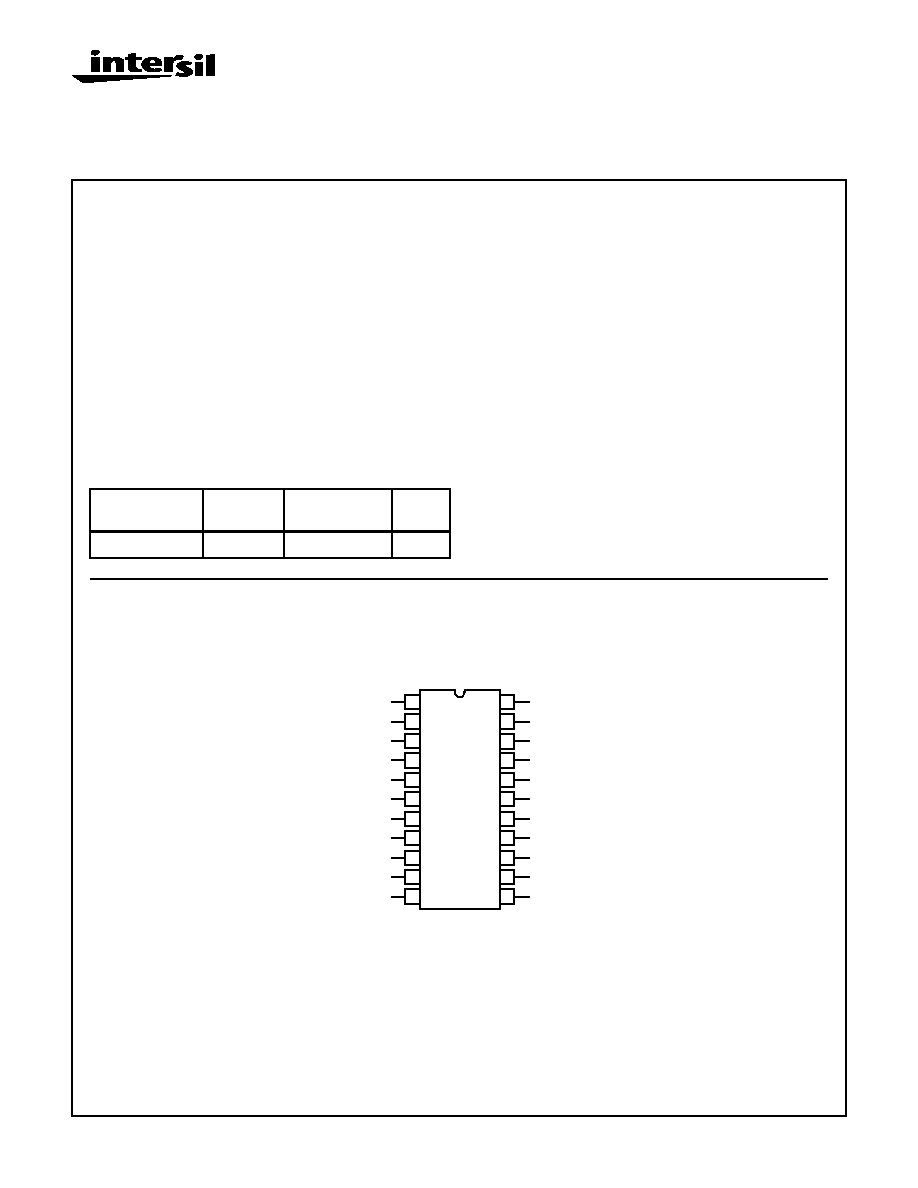
Pinout
CA3224E
(PDIP)
TOP VIEW
Ordering Information
PART NUMBER
TEMP.
RANGE (
o
C)
PACKAGE
PKG.
NO.
CA3224E
-40 to 85
22 Ld PDIP
E22.4
1
11
10
9
8
7
6
5
3
2
4
22
12
13
14
15
16
17
18
19
21
20
CHANNEL 1 INPUT
CHANNEL 1 FREQ COMPENSATION
CHANNEL 2 INPUT
CHANNEL 2 FREQ COMPENSATION
CHANNEL 3 INPUT
CHANNEL 3 FREQ COMPENSATION
GROUND
VERTICAL INPUT
HORIZONTAL INPUT
GRID PULSE OUTPUT
CHANNEL 1 HOLD CAP
CHANNEL 2 HOLD CAP
CHANNEL 2 OUTPUT
CHANNEL 3 HOLD CAP
CHANNEL 1 OUTPUT
CHANNEL 3 OUTPUT
V
REF
BYPASS
AUTO BIAS LEVEL ADJUST
AUTO BIAS PULSE OUTPUT
PROGRAM PULSE OUTPUT
GROUND
V
CC
File Number
1553.1
CAUTION: These devices are sensitive to electrostatic discharge; follow proper IC Handling Procedures.
1-888-INTERSIL or 321-724-7143 | Copyright © Intersil Corporation 1999

8-57
Absolute Maximum Ratings
T
A
= 25
o
C
Thermal Information
Supply Voltage (V
CC
) . . . . . . . . . . . . . . . . . . . . . . . . . . . . . . . . . 11V
DC Input Voltage . . . . . . . . . . . . . . . . . . . . . . . . . . . . . . . . -1 to V
CC
Output Current . . . . . . . . . . . . . . . . . . . . . . . Short Circuit Protected
Operating Conditions
Temperature Range . . . . . . . . . . . . . . . . . . . . . . . . . . -40
o
C to 85
o
C
Supply Voltage Range (Typical) . . . . . . . . . . . . . . . . . . . . 10V
±
10%
Thermal Resistance (Typical, Note 1)
JA
(
o
C/W)
PDIP Package . . . . . . . . . . . . . . . . . . . . . . . . . . . . .
77
Maximum Junction Temperature (Plastic Package) . . . . . . . . 150
o
C
Maximum Storage Temperature Range . . . . . . . . . -65
o
C to 150
o
C
Maximum Lead Temperature (Soldering 10s) . . . . . . . . . . . . . 300
o
C
CAUTION: Stresses above those listed in "Absolute Maximum Ratings" may cause permanent damage to the device. This is a stress only rating and operation
of the device at these or any other conditions above those indicated in the operational sections of this specification is not implied.
NOTE:
1.
JA
is measured with the component mounted on an evaluation PC board in free air.
Electrical Specifications
At T
A
= 25
o
C, V
CC
= 10V, V
BIAS
= 3.75V, V
V
(Pin 8) = V
H
(Pin 10) = 6.0V, S
1
= A, S
2
= A,
See Test Circuit and Timing Diagrams
PARAMETER
TEST PIN NO. SYMBOL
TEST CONDITIONS
MIN
TYP
MAX
UNITS
Supply Current
22
I
CC
-
-
65
mA
Reference Voltage
2, 4, 6
V
REF
Measure at t
4
5.6
6.0
6.4
V
Input Current
2, 4, 6
I
I
V
IN
= 7.2V, S
1
= B
-
-
250
nA
Output Current
Source
17,19, 21
l
OM
+
V
BIAS
= 0.5V, Measure at t
6
, S
1
= B
-
-
-0.8
mA
Sink
l
OM
-
V
BIAS
= 7.0V, Measure at t
6
, S
1
= B
0.8
-
-
mA
Output Buffer
Input Current
17,19, 21
I
I
V
OUT
= 6.5V, V
IN
At pins 16, 18, 20,
Measure at t
4
, S
1
= B
-
-
150
nA
Voltage Gain
A
V
0.97
-
1.07
-
Transconductance
17,19, 21
g
M
Measure at t
6
, V
IN
= 8mV
P-P
at 40kHz, S
1
= B
50
-
100
mS
Auto Bias Pulse
Output Low
13
V
OL
Measure at t
1
-
-
0.3
V
High
V
OH
Measure at t
4
6.05
-
-
V
Current Sink
l
OM
-
Measure at t
4
, S
2
= B
2.5
-
-
mA
Grid Pulse Output
Low
11
V
OL
Measure at t
4
-
-
0.4
V
High
V
OH
Measure at t
1
4.2
-
-
V
Program Pulse Output
Low
12
V
OL
Measure at t
6
-
-
0.4
V
High
V
OH
Measure at t
1
8.2
-
-
V
Vertical Input
8
V
V
See Figure 3
-
6.0
-
V
Horizontal Input
10
V
H
See Figure 3
-
6.0
-
V
Auto Bias Pulse Timing Start
13
t
0
to t
2
, Note 2
835
-
842
µ
s
Finish
t
0
to t
7
, Note 2
1270
-
1275
µ
s
Grid Pulse Timing
Start
11
t
0
to t
3
, Note 2
899
-
905
µ
s
Finish
t
0
to t
5
, Note 2
1080
-
1084
µ
s
Program Pulse Timing
Start
12
t
0
to t
5
, Note 2
1080
-
1084
µ
s
Finish
t
0
to t
7
, Note 2
1270
-
1275
µ
s
NOTE:
2. All time measurements are made from 50% point to 50% point.
CA3224E

8-58
Test Circuit
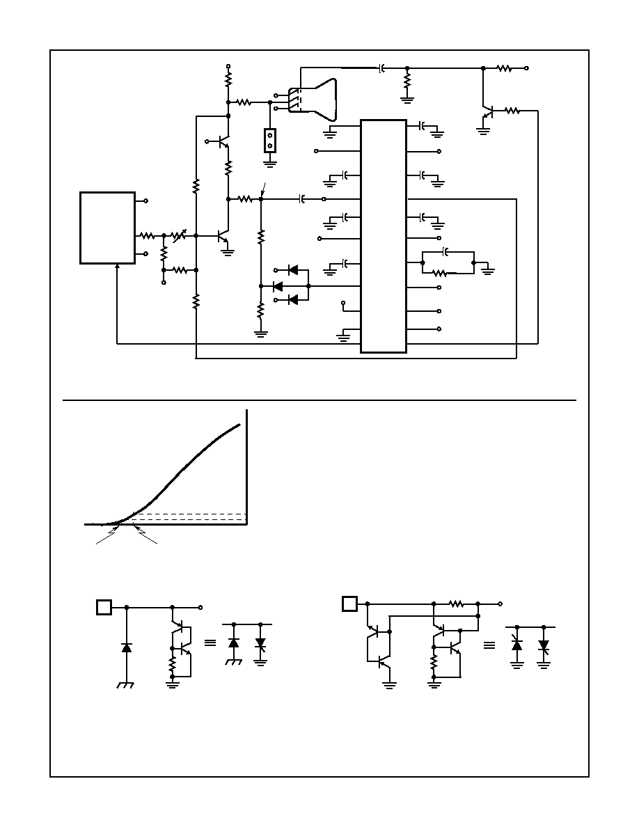
Device Description and Operation
(See Figures 1, 2, 4 and 5)
During the vertical retrace interval, 13 horizontal sync pulses
are counted. On the 14th sync pulse the auto-bias pulse out-
put goes high. This is used to set the RGB drive of the com-
panion chroma/luma circuit to black level. The auto-bias pulse
stays high for 7 horizontal periods during the auto-bias cycle.
On the 15th horizontal sync pulse, the internal logic initiates
the setup interval. During the setup interval, the cathode cur-
rent is increased to a reference value (A in Figure 5) through
the action of the grid pulse. The cathode current causes a
voltage drop across R
S
. This voltage drop, together with the
program pulse output results in a reference voltage at V
S
(summing point) which causes capacitor C
1
to charge to a
voltage proportional to the reference cathode current. The
setup interval lasts for 3 horizontal periods.
On the 18th horizontal sync pulse the grid pulse output goes
high, which through the grid pulse amplifier/inverter, causes
the cathode current to decrease. The decrease in cathode
current results in a positive recovered voltage pulse with
respect to the setup reference level at the V
S
summing point.
The positive recovered voltage pulse is summed with a nega-
tive voltage pulse caused by the program pulse output going
low (cutting off Diode D
1
and switching in resistors R
1
and
R
2
). Any difference between the positive and negative pulses
is fed through capacitor C
1
to the transconductance amplifier.
The difference signal is amplified in the transconductance
amplifier and charges the hold capacitor C
2
, which, through
the buffer amplifier, adjusts the bias on the driver circuit.
Components R
S
, R
1
, and R
2
must be chosen such that the
program pulse and the recovered pulse just cancel at the
desired cathode cutoff level.
V
OUT2
3.65K
0.12
µ
F
A
S
1
B
1
22
21
20
19
18
17
16
15
14
13
12
3.65K
0.12
µ
F
A
S
1
B
V
OUT1
3.65K
0.12
µ
F
A
S
1
B
V
OUT3
47
µ
F
3.32K
+20V
1.50K
+10V
1.5K
A
S
2
B
2
3
4
5
6
7
8
9
10
11
V
IN1
V
IN2
V
IN3
VERTICAL
INPUT
HORIZONTAL
INPUT
CA3224E
0.047
µ
F
0.047
µ
F
0.047
µ
F
20K
1.0K
+
+10V
V
BIAS
CHAN
1 IN
FREQ
COMP
HOLD
CAPACITOR
CHAN
1 OUT
CHAN
2 IN
FREQ
COMP
HOLD
CAPACITOR
CHAN
2 OUT
CHAN
3 IN
FREQ
COMP
HOLD
CAPACITOR
CHAN
3 OUT
2
3
21
20
4
5
19
18
6
7
17
16
x 1
x 1
x 1
+
-
g
M
BUFFER
AMP
AMPLIFER
NO. 3
BUFFER
AMP
AMPLIFER
NO. 2
BUFFER
AMP
AMPLIFER
NO. 1
1
1
2
2
3
3
3
2
1
V
REF
MODE
SWITCH
LOGIC
BIAS
1
9
22
15
8
10
11
12
13
14
GND
GND
V
CC
V
REF
BYPASS
VERT
IN
HORIZ
IN
AUTO
BIAS
LEVEL
ADJUST
AUTO
BIAS
PULSE
OUT
PROG
PULSE
OUT
GRID
PULSE
OUT
MODE SWITCH
STATE
SET-UP
SENSE
OPEN
1
2
3
FIGURE 1. FUNCTIONAL BLOCK DIAGRAM
+
-
g
M
+
-
g
M
CA3224E

8-59
FIGURE 2. FUNCTIONAL TIMING DIAGRAMS
FIGURE 3. VERTICAL AND HORIZONTAL INPUT SIGNALS
VERTICAL INPUT
(PIN 8)
HORIZONTAL INPUT
(PIN 10)
AUTO BIAS
PULSE OUTPUT
(PIN 13)
GRID PULSE OUTPUT
(PIN 11)
PROGRAM PULSE
OUTPUT
(PIN 12)
MODE SWITCH
(SEE FIGURE 1)
OPEN
SET-UP
SENSE
OPEN
t
0
t
1
t
2
t
3
t
4
t
5
t
6
t
7
1
2
3
12
13 14
15
16 17
19
20
22
23
VERTICAL
BLANKING
18
21
16.683ms
V
V
0.5ms
0V
0V
V
H
12
µ
s
63.55
µ
s
VERTICAL SIGNAL
f
H
= 15734.264Hz
HORIZONTAL SIGNAL
f
V
= 59.94Hz
CA3224E
8-60
Electrostatic Protection
(Note)
When correctly designed for ESD protection, SCRs can be
highly effective, enabling circuits to be protected to well in
excess of 4kV. The SCR ESD-EOS protection structures used
on each terminal of the CA3224E are shown schematically in
either Figures 6A or 6B. Although ESD-EOS protection is
included in the CA3224E, proper circuit board layout and
grounding techniques should be observed.
NOTE: For further information on CA3224E protection structures refer
to: AN7304, "Using SCRs as Transient Protection Structures in
Integrated Circuits", by L.R. Avery. Intersil AnswerFAX (407-724-7800)
document #97304.
NOTE:
3. One of three identical driver circuits shown.
FIGURE 4. TYPICAL APPLICATION CIRCUIT
R
G
B
SG
R
IN
0.047
C
C
SUMMING POINT
Q
1
CATH
DRIVE
+12V
R
S
560
1%
200
V
S
R
FB
160K
CHROMA/
CIRCUIT
TO R
DRIVER
BIAS
5K
2.7K
20K
9.1K
TO B
DRIVER
-24V
2.7K
PROGRAM
RGB TO
BLACK LEVEL
R
1
39K
1%
TO R
CH
D
1
TO B
CH
Q
2
BIAS
R
2
62K
1%
+10V
0.047
0.047
B
IN
AUTO-BIAS PULSE
C
1
G
IN
0.12
2.2K
12K
47
µ
F
20K
+
HORIZONTAL
INPUT
VERTICAL
INPUT
AUTO BIAS
LEVEL ADJUST
10
µ
F
B
OUT
+
10
µ
F
+
G
OUT
C
2
R
OUT
+
10
µ
F
+230V
+
33
µ
F
1.5K
3.9K
+10V
10K
Q
3
GRID PULSE
AMPLIFIER
INVERTER
1
21
20
2
19
3
4
18
17
5
CA224E
16
6
15
7
12
14
10
22
9
8
11
13
LUMA
R
G
B
G
IN
FIGURE 5. PICTURE TUBE V-I CURVE
A
B
0
SENSE
V
CATHODE GRID
(V)
SET-UP
(mA)
I
CATHODE
FIGURE 6A.
FIGURE 6B.
FIGURE 6. TRANSIENT PROTECTION
R
HOLD
SUBSTRATE
NEG. TRANSIENT
PROTECT
POSITIVE
TRANSIENT
PROTECT
(A)
TO ACTIVE
CIRCUIT
R
HOLD
R
SENSE
NEGATIVE
TRANSIENT
PROTECT
POSITIVE
TRANSIENT
PROTECT
(B)
TO ACTIVE
CIRCUIT
CA3224E