 | –≠–ª–µ–∫—Ç—Ä–æ–Ω–Ω—ã–π –∫–æ–º–ø–æ–Ω–µ–Ω—Ç: CA3240E | –°–∫–∞—á–∞—Ç—å:  PDF PDF  ZIP ZIP |
1
CA3240, CA3240A
Dual, 4.5MHz, BiMOS Operational Amplifier
with MOSFET Input/Bipolar Output
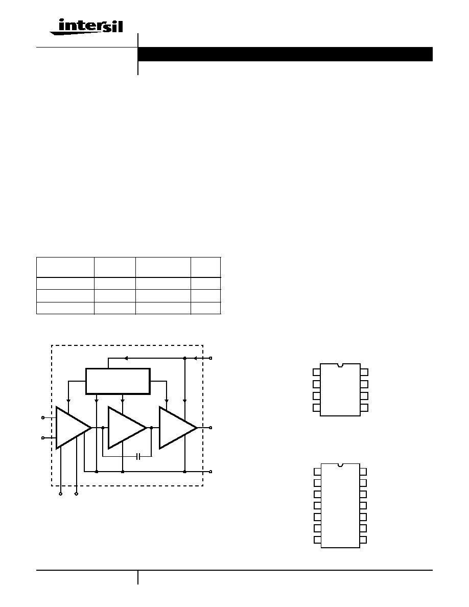
The CA3240A and CA3240 are dual versions of the popular
CA3140 series integrated circuit operational amplifiers. They
combine the advantages of MOS and bipolar transistors on
the same monolithic chip. The gate-protected MOSFET
(PMOS) input transistors provide high input impedance and
a wide common-mode input voltage range (typically to 0.5V
below the negative supply rail). The bipolar output
transistors allow a wide output voltage swing and provide a
high output current capability.
The CA3240A and CA3240 are compatible with the industry
standard 1458 operational amplifiers in similar packages.The
offset null feature is available only when these types are supplied
in the 14 lead PDIP package (E1 suffix).
Functional Diagram
Features
∑ Dual Version of CA3140
∑ Internally Compensated
∑ MOSFET Input Stage
- Very High Input Impedance (Z
IN
) 1.5T
(Typ)
- Very Low Input Current (I
I
) 10pA (Typ) at
±
15V
- Wide Common-Mode Input Voltage Range (V
ICR
): Can
Be Swung 0.5V Below Negative Supply Voltage Rail
∑ Directly Replaces Industry Type 741 in Most Applications
Applications
∑ Ground Referenced Single Amplifiers in Automobile and
Portable Instrumentation
∑ Sample and Hold Amplifiers
∑ Long Duration Timers/Multivibrators (Microseconds-
Minutes-Hours)
∑ Photocurrent Instrumentation
Pinouts
CA3240, CA3240A (PDIP)
TOP VIEW
CA3240A (PDIP)
TOP VIEW
Ordering Information
PART NUMBER
TEMP.
RANGE (
o
C)
PACKAGE
PKG.
NO.
CA3240AE
-40 to 85
8 Ld PDIP
E8.3
CA3240AE1
-40 to 85
14 Ld PDIP
E14.3
CA3240E
-40 to 85
8 Ld PDIP
E8.3
A
10,000
BIAS CIRCUIT
CURRENT SOURCES
AND REGULATOR
A
1
2mA
4mA
2mA
1.6mA
2
µ
A
200
µ
A
200
µ
A
IN-
OUT-
OFFSET NULL
C
1
12pF
V+
V-
+
-
NOTE: Only available with 14 lead DIP (E1 Suffix).
A
10
PUT
PUT
∑ Intrusion Alarm System
∑ Active Filters
∑ Comparators
∑ Function Generators
∑ Instrumentation Amplifiers
∑ Power Supplies
OUTPUT (A)
INV.
INPUT (A)
NON-INV.
1
2
3
4
8
7
6
5
V+
OUTPUT
INV.
NON-INV.
INPUT (A)
V-
INPUT (B)
INPUT (B)
INV.
NON-INV.
OFFSET
V-
OFFSET
NON - INV.
INV.
OFFSET
V+
OUTPUT (A)
NC
OUTPUT (B)
V+
OFFSET
1
2
3
4
5
6
7
14
13
12
11
10
9
8
INPUT (A)
INPUT (A)
NULL (A)
NULL (B)
INPUT (B)
INPUT (B)
NULL (A)
NULL (B)
Pins 9 and 13 internally connected through approximately 3
.
Data Sheet
August 2001
File Number
1050.5
CAUTION: These devices are sensitive to electrostatic discharge; follow proper IC Handling Procedures.
1-888-INTERSIL or 321-724-7143
|
Intersil and Design is a trademark of Intersil Americas Inc.
|
Copyright © Intersil Americas Inc. 2001
2
Absolute Maximum Ratings
Thermal Information
Supply Voltage (Between V+ and V-). . . . . . . . . . . . . . . . . . . . . 36V
Differential Input Voltage . . . . . . . . . . . . . . . . . . . . . . . . . . . . . . . 8V
Input Voltage . . . . . . . . . . . . . . . . . . . . . . . . . (V+ +8V) to (V- -0.5V)
Input Current . . . . . . . . . . . . . . . . . . . . . . . . . . . . . . . . . . . . . . . 1mA
Output Short Circuit Duration (Note 1). . . . . . . . . . . . . . . . Indefinite
Operating Conditions
Temperature Range . . . . . . . . . . . . . . . . . . . . . . . . . . -40
o
C to 85
o
C
Voltage Range . . . . . . . . . . . . . . . . . . . . . 4V to 36V or
±
2V to
±
18V
Thermal Resistance (Typical, Note 2)
JA
(
o
C/W)
8 Lead PDIP Package . . . . . . . . . . . . . . . . . . . . . . .
100
14 Lead PDIP Package . . . . . . . . . . . . . . . . . . . . . .
100
Maximum Junction Temperature (Plastic Package) . . . . . . . 150
o
C
Maximum Storage Temperature Range . . . . . . . . . . -65
o
C to 150
o
C
Maximum Lead Temperature (Soldering 10s) . . . . . . . . . . . . 300
o
C
CAUTION: Stresses above those listed in "Absolute Maximum Ratings" may cause permanent damage to the device. This is a stress only rating and operation of the
device at these or any other conditions above those indicated in the operational sections of this specification is not implied.
NOTES:
1. Short circuit may be applied to ground or to either supply. Temperatures and/or supply voltages must be limited to keep dissipation within max-
imum rating.
2.
JA
is measured with the component mounted on an evaluation PC board in free air.
Electrical Specifications
For Equipment Design, V
SUPPLY
=
±
15V, T
A
= 25
o
C, Unless Otherwise Specified
PARAMETER
SYMBOL
CA3240
CA3240A
UNITS
MIN
TYP
MAX
MIN
TYP
MAX
Input Offset Voltage
V
IO
-
5
15
-
2
5
mV
Input Offset Current
I
IO
-
0.5
30
-
0.5
20
pA
Input Current
I
I
-
10
50
-
10
40
pA
Large-Signal Voltage Gain
(See Figures 13, 28) (Note 3)
A
OL
20
100
-
20
100
-
kV/V
86
100
-
86
100
-
dB
Common Mode Rejection
Ratio (See Figure 18)
CMRR
-
32
320
-
32
320
µ
V/V
70
90
-
70
90
-
dB
Common Mode Input Voltage Range
(See Figure 25)
V
ICR
-15
-15.5 to
+12.5
11
-15
-15.5 to
+12.5
12
V
Power Supply Rejection Ratio
(See Figure 20)
PSRR
(
V
IO
/
V
±)
-
100
150
-
100
150
µ
V/V
76
80
-
76
80
-
dB
Maximum Output Voltage (Note 4)
(See Figures 24, 25)
V
OM
+
12
13
-
12
13
-
V
V
OM
-
-14
-14.4
-
-14
-14.4
-
V
Maximum Output Voltage (Note 5)
V
OM-
0.4
0.13
-
0.4
0.13
-
V
Total Supply Current
(See Figure 16) For Both Amps
I+
-
8
12
-
8
12
mA
Total Device Dissipation
P
D
-
240
360
-
240
360
mW
NOTES:
3. At V
O
= 26V
P-P
, +12V, -14V and R
L
= 2k
.
4. At R
L
= 2k
.
5. At V+ = 5V, V- = GND, I
SINK
= 200
µ
A.
Electrical Specifications
For Equipment Design, V
SUPPLY
=
±
15V, T
A
= 25
o
C, Unless Otherwise Specified
PARAMETER
SYMBOL
TEST CONDITIONS
TYPICAL VALUES
UNITS
CA3240A
CA3240
Input Offset Voltage Adjustment Resistor (E1
Package Only)
Typical Value of Resistor Between Terminals 4 and 3(5)
or Between 4 and 14(8) to Adjust Maximum V
IO
18
4.7
k
Input Resistance
R
I
1.5
1.5
T
Input Capacitance
C
I
4
4
pF
Output Resistance
R
O
60
60
Equivalent Wideband Input Noise Voltage
(See Figure 2)
e
N
BW = 140kHz, R
S
= 1M
48
48
µ
V
CA3240, CA3240A

3
Equivalent Input Noise Voltage
(See Figure 19)
e
N
f = 1kHz, R
S
= 100
40
40
nV/
Hz
f = 10kHz, R
S
= 100
12
12
nV/
Hz
Short-Circuit Current to Opposite Supply
I
OM
+
Source
40
40
mA
I
OM
-
Sink
11
11
mA
Gain Bandwidth Product (See Figures 14, 28)
f
T
4.5
4.5
MHz
Slew Rate (See Figure 15)
SR
9
9
V/
µ
s
Transient Response (See Figure 1)
t
r
R
L
= 2k
, C
L
= 100pF
Rise Time
0.08
0.08
µ
s
OS
R
L
= 2k
, C
L
= 100pF
Overshoot
10
10
%
Settling Time at 10V
P-P
(See Figure 26)
t
S
A
V
= +1, R
L
= 2k
, C
L
= 100pF,
Voltage Follower
To 1mV
4.5
4.5
µ
s
To 10mV
1.4
1.4
µ
s
Crosstalk (See Figure 23)
f = 1kHz
120
120
dB
Electrical Specifications
For Equipment Design, V
SUPPLY
=
±
15V, T
A
= 25
o
C, Unless Otherwise Specified (Continued)
PARAMETER
SYMBOL
TEST CONDITIONS
TYPICAL VALUES
UNITS
CA3240A
CA3240
Electrical Specifications
For Equipment Design, at V
SUPPLY
=
±
15V, T
A
= -40 to 85
o
C, Unless Otherwise Specified
PARAMETER
SYMBOL
TYPICAL VALUES
UNITS
CA3240A
CA3240
Input Offset Voltage
|V
IO
|
3
10
mV
Input Offset Current (Note 8)
|I
IO
|
32
32
pA
Input Current (Note 8)
I
I
640
640
pA
Large Signal Voltage Gain (See Figures 13, 28), (Note 6)
A
OL
63
63
kV/V
96
96
dB
Common Mode Rejection Ratio (See Figure 18)
CMRR
32
32
µ
V/V
90
90
dB
Common Mode Input Voltage Range (See Figure 25)
V
ICR
-15 to +12.3
-15 to +12.3
V
Power Supply Rejection Ratio (See Figure 20)
PSRR
(
V
IO
/
V
±
)
150
150
µ
V/V
76
76
dB
Maximum Output Voltage (Note 7) (See Figures 24, 25)
V
OM
+
12.4
12.4
V
V
OM
-
-14.2
-14.2
V
Supply Current (See Figure 16) Total For Both Amps
I+
8.4
8.4
mA
Total Device Dissipation
P
D
252
252
mW
Temperature Coefficient of Input Offset Voltage
V
IO
/
T
15
15
µ
V/
o
C
NOTES:
6. At V
O
= 26V
P-P
, +12V, -14V and R
L
= 2k
.
7. At R
L
= 2k
.
8. At T
A
= 85
o
C.
Electrical Specifications
For Equipment Design, at V+ = 5V, V- = 0V, T
A
= 25
o
C, Unless Otherwise Specified
PARAMETER
SYMBOL
TYPICAL VALUES
UNITS
CA3240A
CA3240
Input Offset Voltage
|V
IO
|
2
5
mV
Input Offset Current
|I
IO
|
0.1
0.1
pA
Input Current
I
I
2
2
pA
Input Resistance
R
IN
1
1
T
Large Signal Voltage Gain (See Figures 13, 28)
A
OL
100
100
kV/V
100
100
dB
CA3240, CA3240A
4
Common-Mode Rejection Ratio
CMRR
32
32
µ
V/V
90
90
dB
Common-Mode Input Voltage Range (See Figure 25)
V
ICR
-0.5
-0.5
V
2.6
2.6
V
Power Supply Rejection Ratio
PSRR
31.6
31.6
µ
V/V
90
90
dB
Maximum Output Voltage (See Figures 24, 25)
V
OM
+
3
3
V
V
OM
-
0.3
0.3
V
Maximum Output Current
Source
I
OM
+
20
20
mA
Sink
I
OM
-
1
1
mA
Slew Rate (See Figure 15)
SR
7
7
V/
µ
s
Gain Bandwidth Product (See Figure 14)
f
T
4.5
4.5
MHz
Supply Current (See Figure 16)
I+
4
4
mA
Device Dissipation
P
D
20
20
mW
Electrical Specifications
For Equipment Design, at V+ = 5V, V- = 0V, T
A
= 25
o
C, Unless Otherwise Specified (Continued)
PARAMETER
SYMBOL
TYPICAL VALUES
UNITS
CA3240A
CA3240
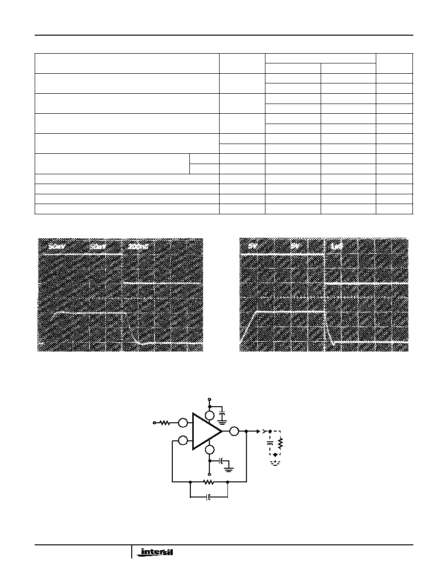
Test Circuits and Waveforms
FIGURE 1A. SMALL SIGNAL RESPONSE
FIGURE 1B. LARGE SIGNAL RESPONSE
FIGURE 1C. TEST CIRCUIT
FIGURE 1. SPLIT-SUPPLY VOLTAGE FOLLOWER TEST CIRCUIT AND ASSOCIATED WAVEFORMS
50mV/Div., 200ns/Div.
Top Trace: Input, Bottom Trace: Output
5V/Div., 1
µ
s/Div.
Top Trace: Input, Bottom Trace: Output
2k
10k
CA3240
+15V
-15V
0.1
µ
F
0.1
µ
F
100pF
SIMULATED
LOAD
2k
0.05
µ
F
+
-
BW (-3dB) = 4.5MHz
SR = 9V/
µ
s
CA3240, CA3240A

5
Schematic Diagram
(One Amplifier of Two)
FIGURE 2. TEST CIRCUIT AMPLIFIER (30dB GAIN) USED FOR WIDEBAND NOISE MEASUREMENT
Test Circuits and Waveforms
(Continued)
R
S
CA3240
+15V
-15V
0.01
µ
F
0.01
µ
F
+
-
BW (-3dB) = 140kHz
TOTAL NOISE VOLTAGE
30.1k
1k
1M
(REFERRED TO INPUT) = 48
µ
V (TYP)
NOISE
VOLTAGE
OUTPUT
BIAS CIRCUIT
INPUT STAGE
SECOND STAGE
OUTPUT STAGE
DYNAMIC CURRENT SINK
V+
OUTPUT
V-
OFFSET NULL (NOTE 9)
INVERTING
INPUT
NON-INVERTING
INPUT +
-
R
1
8K
Q
1
D
1
Q
6
Q
7
Q
8
Q
2
Q
5
Q
4
Q
3
D
2
D
3
D
4
D
5
Q
9
Q
10
R
2
500
R
5
500
R
4
500
R
3
500
Q
11
Q
12
Q
13
C
1
12pF
Q
14
R
6
50
R
7
30
Q
15
Q
16
R
8
1K
R
11
20
Q
17
R
10
1K
R
9
50
D
7
D
8
Q
20
Q
21
R
12
12K
R
14
20K
R
13
15K
D
6
Q
18
Q
19
NOTES:
9. Only available with 14 Lead DIP (E1 Suffix).
10. All resistance values are in ohms.
CA3240, CA3240A