 | –≠–ª–µ–∫—Ç—Ä–æ–Ω–Ω—ã–π –∫–æ–º–ø–æ–Ω–µ–Ω—Ç: CA3260 | –°–∫–∞—á–∞—Ç—å:  PDF PDF  ZIP ZIP |
1
CA3260, CA3260A
4MHz, BiMOS Operational Amplifier with
MOSFET Input/CMOS Output
CA3260A and CA3260 are integrated circuit operational
amplifiers that combine the advantage of both CMOS and
bipolar transistors on a monolithic chip. The CA3260 series
circuits are dual versions of the popular CA3160 series.
Gate protected P-Channel MOSFET (PMOS) transistors are
used in the input circuit to provide very high input
impedance, very low input current, and exceptional speed
performance. The use of PMOS field effect transistors in the
input stage results in common mode input voltage capability
down to 0.5V below the negative supply terminal, an
important attribute in single supply applications.
A complementary symmetry MOS (CMOS) transistor pair,
capable of swinging the output voltage to within 10mV of
either supply voltage terminal (at very high values of load
impedance), is employed as the output circuit.
The CA3260 Series circuits operate at supply voltages
ranging from 4V to 16V, or
±
2V to
±
8V when using split
supplies. The CA3260A offers superior input characteristics
over those of the CA3260.
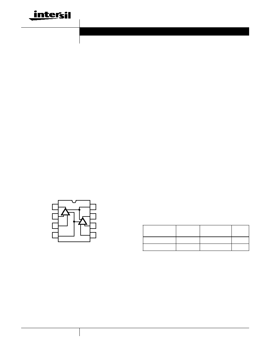
Pinout
CA3260, CA3260A (PDIP)
TOP VIEW
Features
∑ MOSFET Input Stage provides
- Very High Z
I
= 1.5T
(1.5 x 10
12
) (Typ)
- Very Low I
I
. . . . . . . . . . . . 5pA (Typ) at 15V Operation
. . . . . . . . . . . . . . . . . . . . . . 2pA (Typ) at 5V Operation
∑ Ideal for Single Supply Applications
∑ Common Mode Input Voltage Range Includes
Negative Supply Rail; Input Terminals Can be Swung 0.5V
Below Negative Supply Rail
∑ CMOS Output Stage Permits Signal Swing to Either (Or
Both) Supply Rails
Applications
∑ Ground Referenced Single Supply Amplifiers
∑ Fast Sample-Hold Amplifiers
∑ Long Duration Timers/Monostables
∑ Ideal Interface with Digital CMOS
∑ High Input Impedance Wideband Amplifiers
∑ Voltage Followers (e.g. Follower for Single Supply D/A
Converter)
∑ Voltage Regulators (Permits Control of Output Voltage
Down to 0V)
∑ Wien Bridge Oscillators
∑ Voltage Controlled Oscillators
∑ Photo Diode Sensor Amplifiers
NON INV. INPUT (A)
V-
1
2
3
8
7
6
5
V+
OUTPUT (B)
INV. INPUT (B)
NON INV. INPUT (B)
OUTPUT (A)
A
4
B
+
-
+
-
INV. INPUT (A)
Ordering Information
PART NUMBER
TEMP.
RANGE (
o
C)
PACKAGE
PKG.
NO.
CA3260E
-55 to 125
8 Ld PDIP
E8.3
CA3260AE
-55 to 125
8 Ld PDIP
E8.3
Data Sheet
September 1998
File Number
1266.4
CAUTION: These devices are sensitive to electrostatic discharge; follow proper IC Handling Procedures.
1-888-INTERSIL or 321-724-7143
|
Copyright
©
Intersil Corporation 1999
2
Absolute Maximum Ratings
Thermal Information
DC Supply Voltage (V+ to V-). . . . . . . . . . . . . . . . . . . . . . . . . . . 16V
DC Input Voltage . . . . . . . . . . . . . . . . . . . . . . (V+ +8V) to (V- -0.5V)
Differential Input Voltage . . . . . . . . . . . . . . . . . . . . . . . . . . . . . . . 8V
Input Terminal Current . . . . . . . . . . . . . . . . . . . . . . . . . . . . . . . . 1mA
Output Short Circuit Duration (Note 1). . . . . . . . . . . . . . . . Indefinite
Operating Conditions
Temperature Range . . . . . . . . . . . . . . . . . . . . . . . . . -55
o
C to 125
o
C
Thermal Resistance (Typical, Note 2)
JA
(
o
C/W)
JC
(
o
C/W)
PDIP Package . . . . . . . . . . . . . . . . . . .
100
N/A
Maximum Junction Temperature (Plastic Package) . . . . . . . .150
o
C
Maximum Storage Temperature Range . . . . . . . . . . -65
o
C to 150
o
C
Maximum Lead Temperature (Soldering 10s) . . . . . . . . . . . . 300
o
C
CAUTION: Stresses above those listed in "Absolute Maximum Ratings" may cause permanent damage to the device. This is a stress only rating and operation of the
device at these or any other conditions above those indicated in the operational sections of this specification is not implied.
NOTES:
1. Short circuit may be applied to ground or to either supply.
2.
JA
is measured with the component mounted on an evaluation PC board in free air.
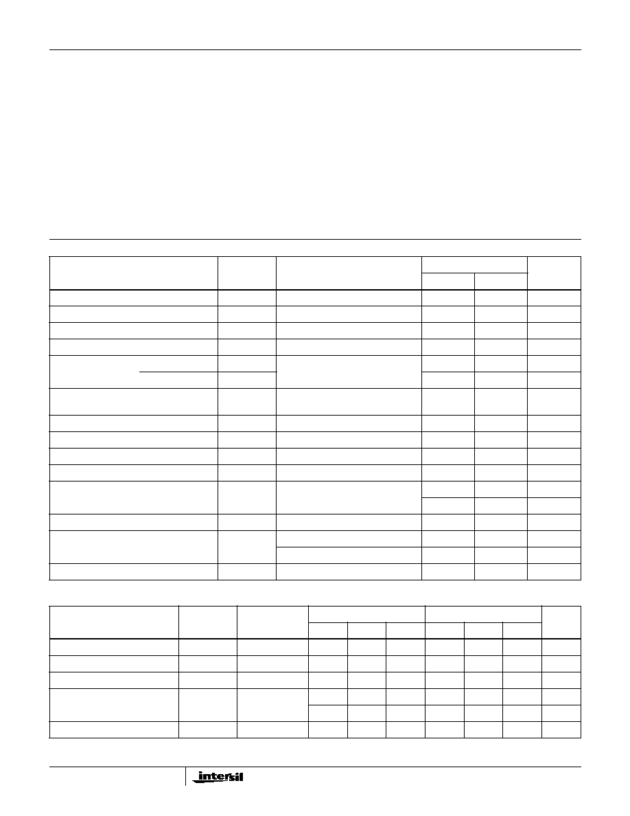
Electrical Specifications
T
A
= 25
o
C, Typical Values Intended Only for Design Guidance
PARAMETER
SYMBOL
TEST CONDITIONS
TYPICAL VALUES
UNITS
CA3260A
CA3260
Input Resistance
RI
V
S
=
±
7.5V
1.5
1.5
T
Input Capacitance
C
I
f = 1MHz, V
S
=
±
7.5V
4.3
4.3
pF
Unity Gain Crossover Frequency
f
T
V
S
=
±
7.5V
4
4
MHz
Slew Rate
SR
V
S
=
±
7.5V
10
10
V/
µ
s
Transient Response
Rise Time
t
r
C
L
= 25pF, R
L
= 2k
,
A
V
= +1,
V
S
=
±
7.5V
0.09
0.09
µ
s
Overshoot
OS
10
10
%
Settling Time (to <0.1
%
, V
IN
= 4V
P-P
)
t
S
C
L
= 25pF, R
L
= 2k
,
A
V
= +1,
V
S
=
±
7.5V
1.8
1.8
µ
s
Input Offset Voltage
V
IO
V+ = 5V, V- = 0V
2
6
mV
Input Offset Current
I
IO
V+ = 5V, V- = 0V
0.1
0.1
pA
Input Current
I
I
V+ = 5V, V- = 0V
2
2
pA
Common Mode Rejection Ratio
CMRR
V+ = 5V, V- = 0V
70
60
dB
Large Signal Voltage Gain
A
OL
V
O
= 4V
P-P
, R
L
= 20k
,
V+ = 5V, V- = 0V
100
100
kV/V
100
100
dB
Common Mode Input Voltage Range
V
ICR
V+ = 5V, V- = 0V
0 to 2.5
0 to 2.5
V
Supply Current
I+
V
O
= 5V, R
L
=
,
V+ = 5V, V- = 0V
1
1
mA
V
O
= 2.5V, R
L
=
,
V+ = 5V, V- = 0V
1.2
1.2
mA
Power Supply Rejection Ratio
PSRR
V
IO
/
V+, V+ = 5V, V- = 0V
200
200
µ
V/V
Electrical Specifications
For Each Amplifier at T
A
= 25
o
C, V+ = 15V, V- = 0V, Unless Otherwise Specified
PARAMETER
SYMBOL
TEST
CONDITIONS
CA3260A
CA3260
UNITS
MIN
TYP
MAX
MIN
TYP
MAX
Input Offset Voltage
|V
IO
|
V
S
=
±
7.5V
-
2
5
-
6
15
mV
Input Offset Current
|I
IO
|
V
S
=
±
7.5V
-
0.5
20
-
0.5
30
pA
Input Current
I
I
V
S
=
±
7.5V
-
5
30
-
5
50
pA
Large Signal Voltage Gain
A
OL
V
O
= 10V
P-P
,
R
L
= 10k
50
320
-
50
320
-
kV/V
94
110
-
94
110
-
dB
Common Mode Rejection Ratio
CMRR
80
95
-
70
90
-
dB
CA3260, CA3260A
3
All Intersil semiconductor products are manufactured, assembled and tested under ISO9000 quality systems certification.
Intersil semiconductor products are sold by description only. Intersil Corporation reserves the right to make changes in circuit design and/or specifications at any time with-
out notice. Accordingly, the reader is cautioned to verify that data sheets are current before placing orders. Information furnished by Intersil is believed to be accurate and
reliable. However, no responsibility is assumed by Intersil or its subsidiaries for its use; nor for any infringements of patents or other rights of third parties which may result
from its use. No license is granted by implication or otherwise under any patent or patent rights of Intersil or its subsidiaries.
For information regarding Intersil Corporation and its products, see web site http://www.intersil.com
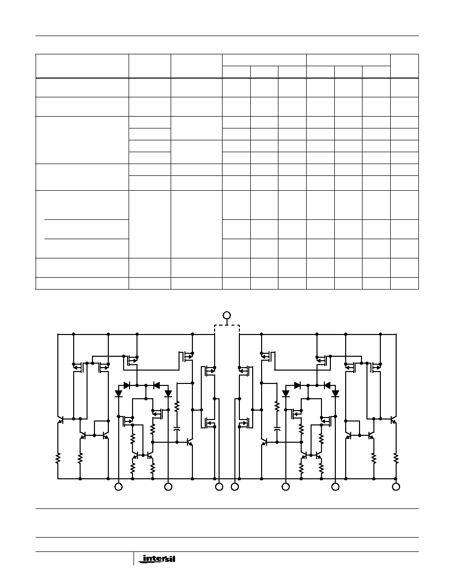
Schematic Diagram
Common Mode Input Voltage
Range
V
lCR
0
-0.5 to
12
10
0
-0.5 to
12
10
V
Power Supply Rejection Ratio
PSRR
V
IO
/
V+
V+ = 17.5V
-
32
150
-
32
320
µ
V/V
Maximum Output Voltage
V
OM
+
R
L
= 10k
11
13.3
-
11
13.3
-
V
V
OM
-
-
0.002
0.01
-
0.002
0.01
V
V
OM
+
R
L
=
14.99
15
-
14.99
15
-
V
V
OM
-
-
0
0.01
-
0
0.01
V
Maximum Output Current
I
OM
+ Source
V
O
= 7.5V
12
22
45
12
22
45
mA
I
OM
- Sink
12
20
45
12
20
45
mA
Total Supply Current
I+
R
L
=
V
O
(Amplifier A) = 7.5V
V
O
(Amplifier B) = 7.5V
-
9
15.5
-
9
15.5
mA
V
O
(Amplifier A) = 0V
V
O
(Amplifier B) = 0V
-
1.2
3
-
1.2
3
mA
V
O
(Amplifier A) = 0V
V
O
(Amplifier B) = 7.5V
-
5
8.5
-
5
8.5
mA
Input Offset Voltage
Temperature Drift
V
IO
/
T
-
6
-
-
8
-
µ
V/
o
C
Crosstalk
f = 1kHz
-
120
-
-
120
-
dB
Electrical Specifications
For Each Amplifier at T
A
= 25
o
C, V+ = 15V, V- = 0V, Unless Otherwise Specified (Continued)
PARAMETER
SYMBOL
TEST
CONDITIONS
CA3260A
CA3260
UNITS
MIN
TYP
MAX
MIN
TYP
MAX
R
6
200K
R
7
300K
Q
12
Q
11
Q
10
D
2
D
3
D
4
D
1
Q
1
Q
2
Q
6
R
4
1K
R
2
1K
R
1
1K
R
3
1K
Q
13
Q
14
Q
3
Q
4
C
1
30pF
R
5
2K
Q
7
Q
9
3
2
1
Q
5
Q
8
AMPLIFIER A
R
13
200K
R
14
300
Q
26
Q
25
Q
24
D
7
D
6
D
5
D
8
Q
15
Q
16
Q
20
R
11
1K
R
9
1K
R
8
1K
R
10
1K
Q
27
Q
28
Q
17
Q
18
C
2
30pF
R
12
2K
Q
21
Q
23
5
6
7
Q
19
Q
22
AMPLIFIER B
4
8 V+
CA3260, CA3260A