 | –≠–ª–µ–∫—Ç—Ä–æ–Ω–Ω—ã–π –∫–æ–º–ø–æ–Ω–µ–Ω—Ç: CA3318CE | –°–∫–∞—á–∞—Ç—å:  PDF PDF  ZIP ZIP |

4-9
August 1997
CA3318
CMOS Video Speed,
8-Bit, Flash A/D Converter
File Number
3103.1
Features
∑ CMOS Low Power with SOS Speed (Typ). . . . . . . . 150mW
∑ Parallel Conversion Technique
∑ 15MHz Sampling Rate (Conversion Time) . . . . . . . 67ns
∑ 8-Bit Latched Three-State Output with Overflow Bit
∑ Accuracy (Typ) . . . . . . . . . . . . . . . . . . . . . . . . . .
±
1 LSB
∑ Single Supply Voltage . . . . . . . . . . . . . . . . . . 4V to 7.5V
∑ 2 Units in Series Allow 9-Bit Output
∑ 2 Units in Parallel Allow 30MHz Sampling Rate
Applications
∑ TV Video Digitizing (Industrial/Security/Broadcast)
∑ High Speed A/D Conversion
∑ Ultrasound Signature Analysis
∑ Transient Signal Analysis
∑ High Energy Physics Research
∑ General-Purpose Hybrid ADCs
∑ Optical Character Recognition
∑ Radar Pulse Analysis
∑ Motion Signature Analysis
∑
µ
P Data Acquisition Systems
Description
The CA3318 is a CMOS parallel (FLASH) analog-to-digital
converter designed for applications demanding both low
power consumption and high speed digitization.
The CA3318 operates over a wide full scale input voltage
range of 4V up to 7.5V with maximum power consumption
depending upon the clock frequency selected. When
operated from a 5V supply at a clock frequency of 15MHz,
the typical power consumption of the CA3318 is 150mW.
The intrinsic high conversion rate makes the CA3318 ideally
suited for digitizing high speed signals. The overflow bit
makes possible the connection of two or more CA3318s in
series to increase the resolution of the conversion system. A
series connection of two CA3318s may be used to produce a
9-bit high speed converter. Operation of two CA3318s in
parallel doubles the conversion speed (i.e., increases the
sampling rate from 15MHz to 30MHz).
256 paralleled auto balanced voltage comparators measure
the input voltage with respect to a known reference to
produce the parallel bit outputs in the CA3318.
255 comparators are required to quantize all input voltage
levels in this 8-bit converter, and the additional comparator is
required for the overflow bit.
Ordering Information
Pinout
CA3318
(PDIP, SBDIP, SOIC)
TOP VIEW
PART NUMBER LINEARITY (INL, DNL)
SAMPLING RATE
TEMP. RANGE (
o
C)
PACKAGE
PKG. NO.
CA3318CE
±
1.5 LSB
15MHz (67ns)
-40 to 85
24 Ld PDIP
E24.6
CA3318CM
±
1.5 LSB
15MHz (67ns)
-40 to 85
24 Ld SOIC
M24.3
CA3318CD
±
1.5 LSB
15MHz (67ns)
-40 to 85
24 Ld SBDIP
D24.6
1
2
3
4
5
6
7
8
9
10
11
12
16
17
18
19
20
21
22
23
24
15
14
13
(LSB) B1
B2
B3
B4
B5
B6
B7
(MSB) B8
OVERFLOW
1
/
4
R
(DIG. GND) V
SS
(DIG. SUP.) V
DD
V
AA
+ (ANA. SUP.)
V
REF
+
V
IN
p
PHASE
V
AA
- (ANA. GND)
V
REF
-
CE1
CE2
3
/
4
R
CLK
V
IN
CAUTION: These devices are sensitive to electrostatic discharge; follow proper IC Handling Procedures.
http://www.intersil.com or 407-727-9207
|
Copyright
©
Intersil Corporation 1999

4-10
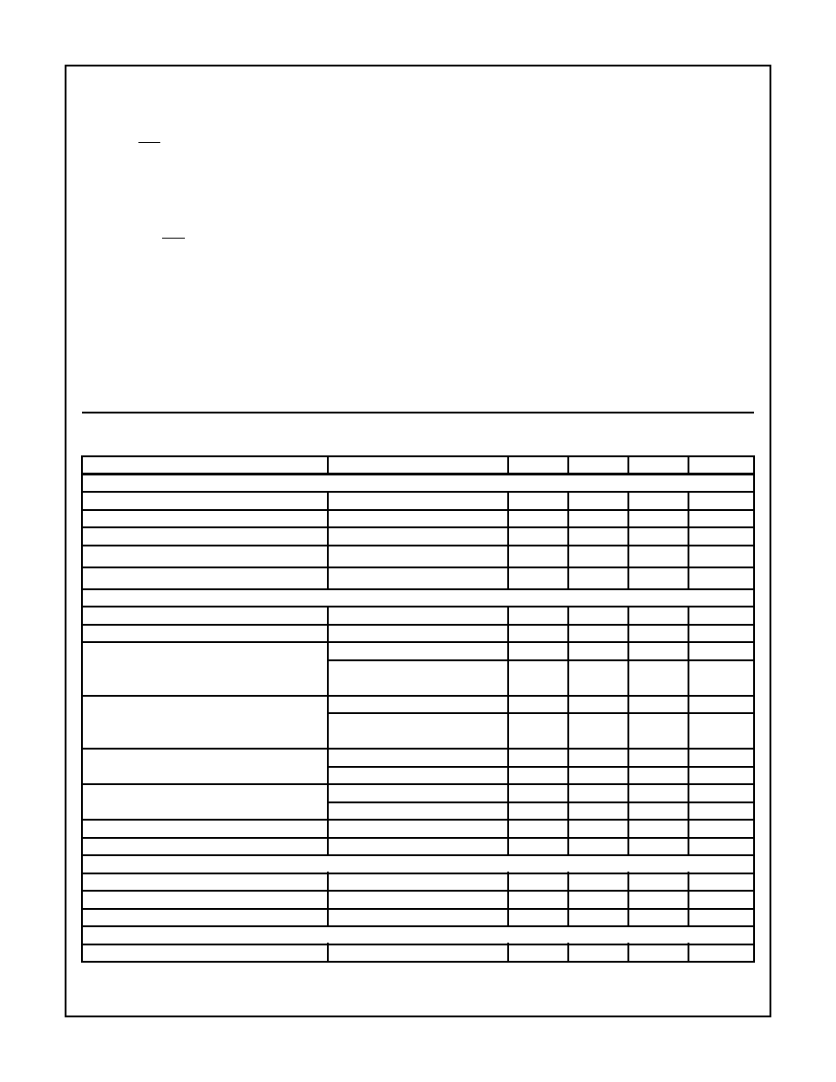
Functional Block Diagram
LATCH
256
D
Q
ENCODER
LOGIC
ARRAY
CLK
D Q
CLK
D Q
CLK
D Q
CLK
D Q
CLK
D Q
CLK
D Q
CLK
D Q
CLK
D Q
CLK
D Q
CAB
LATCH
D
Q
D
Q
COUNT
193
CAB
LATCH
D
Q
D
Q
COUNT
129
CAB
LATCH
D
Q
D
Q
COUNT
65
CAB
LATCH
1
D
Q
LATCH
11
D
Q
COUNT
1
CAB
# 256
# 193
# 129
# 65
23
3
/
4
REF
20
1
/
2
REF
10
1
/
4
REF
22
21
24
16
15
V
REF
+
V
IN
V
AA
+
V
IN
V
REF
-
(NOTE 1)
COMPARATOR #1
LATCH
LATCH
LATCH
9
OVER-
FLOW
THREE-
STATE
DRIVERS
OUTPUT
REGISTER
DIGITAL
SUPPLY
12
V
DD
2
1
1
1
1
2
1
8
BIT 8
(MSB)
7
BIT 7
6
BIT 6
5
BIT 5
4
BIT 4
3
BIT 3
2
BIT 2
1
BIT 1
(LSB)
14
CE1
13
CE2
DIGITAL
GND
11
V
SS
18
CLOCK
19
PHASE
17
V
AA
-
ANALOG
GND
1 (AUTO BALANCE)
2 (SAMPLE UNKNOWN)
NOTE:
50K
1
/
2
R
= 4
= 30
= 7
R = 2
R
R
R
R
R
R
2K
ANALOG
SUPPLY
1
/
2
R
R
LATCH
256
COUNT
256
D
Q
1. Cascaded Auto Balance (CAB).
CA3318
4-11
Absolute Maximum Ratings
Thermal Information
DC Supply Voltage Range (V
DD
or V
AA
+) . . . . . . . . . . -0.5V to +8V
(Referenced to V
SS
or V
AA
- Terminal, Whichever is More Negative)
Input Voltage Range
CE2 and CE1 . . . . . . . . . . . . . . . . . . . . V
AA
- -0.5V to V
DD
+ 0.5V
Clock, Phase, V
REF
-,
1
/
2
Ref . . . . . . . V
AA
- -0.5V to V
AA
+ + 0.5V
Clock, Phase, V
REF
-,
1
/
4
Ref . . . . . . . . V
SS
- -0.5V to V
DD
+ 0.5V
V
IN
,
3
/
4
REF, V
REF
+ . . . . . . . . . . . . . . V
AA
- -0.5V to V
AA
- + 7.5V
Output Voltage Range, . . . . . . . . . . . . . . . V
SS
- 0.5V to V
DD
+ 0.5V
Bits 1-8, Overflow (Outputs Off)
DC Input Current . . . . . . . . . . . . . . . . . . . . . . . . . . . . . . . . .
±
20mA
Clock, Phase, CE1, CE2, V
IN
, Bits 1-8, Overflow
Operating Conditions
Operating Voltage Range (V
DD
or V
AA
+) . . . 4V (Min) to 7.5V (Max)
Recommended V
AA
+ Operating Range . . . . . . . . . . . . . . . V
DD
±
1V
Recommended V
AA
- Operating Range . . . . . . . . . . . . . . . V
SS
±
1V
Operating Temperature Range (T
A
) . . . . . . . . . . . . . . -40
o
C to 85
o
C
Thermal Resistance (Typical, Note 1)
JA
(
o
C/W)
JC
(
o
C/W)
SBDIP Package . . . . . . . . . . . . . . . . . . . .
60
22
PDIP Package . . . . . . . . . . . . . . . . . . . . .
60
N/A
SOIC Package . . . . . . . . . . . . . . . . . . . . .
75
N/A
Maximum Junction Temperature
Ceramic Package . . . . . . . . . . . . . . . . . . . . . . . . . . . . . . . . 175
o
C
Plastic Packages . . . . . . . . . . . . . . . . . . . . . . . . . . . . . . . . . 150
o
C
Maximum Storage Temperature Range . . . . . . . . . .-65
o
C to 150
o
C
Maximum Lead Temperature (Soldering 10s) . . . . . . . . . . . . . 265
o
C
(SOIC - Lead Tips Only)
CAUTION: Stresses above those listed in "Absolute Maximum Ratings" may cause permanent damage to the device. This is a stress only rating and operation
of the device at these or any other conditions above those indicated in the operational sections of this specification is not implied.
NOTE:
1.
JA
is measured with the component mounted on an evaluation PC board in free air.
Electrical Specifications
At 25
o
C, V
AA
+ = V
DD
= 5V, V
REF
+ = 6.4V, V
REF
- = V
AA
- = V
SS
, CLK = 15MHz,
All Reference Points Adjusted, Unless Otherwise Specified
PARAMETER
TEST CONDITIONS
MIN
TYP
MAX
UNITS
SYSTEM PERFORMANCE
Resolution
8
-
-
Bits
Integral Linearity Error
-
-
±
1.5
LSB
Differential Linearity Error
-
-
+1, -0.8
LSB
Offset Error, Unadjusted
V
IN
= V
REF
- +
1
/
2
LSB
-0.5
4.5
6.4
LSB
Gain Error Unadjusted
V
IN
= V
REF
+ -
1
/
2
LSB
-1.5
0
1.5
LSB
DYNAMIC CHARACTERISTICS
Maximum Input Bandwidth
(Note 1) CA3318
2.5
5.0
-
MHz
Maximum Conversion Speed
CLK = Square Wave
15
17
-
MSPS
Signal to Noise Ratio (SNR)
f
S
= 15MHz, f
IN
= 100kHz
-
47
-
dB
f
S
= 15MHz, f
IN
= 4MHz
-
43
-
dB
Signal to Noise Ratio (SINAD)
f
S
= 15MHz, f
IN
= 100kHz
-
45
-
dB
f
S
= 15MHz, f
IN
= 4MHz
-
35
-
dB
Total Harmonic Distortion, THD
f
S
= 15MHz, f
IN
= 100kHz
-
-46
-
dBc
f
S
= 15MHz, f
IN
= 4MHz
-
-36
-
dBc
Effective Number of Bits (ENOB)
f
S
= 15MHz, f
IN
= 100kHz
-
7.2
-
Bits
f
S
= 15MHz, f
IN
= 4MHz
-
5.5
-
Bits
Differential Gain Error
Unadjusted
-
2
-
%
Differential Phase Error
Unadjusted
-
1
-
%
ANALOG INPUTS
Full Scale Range, V
IN
and (V
REF
+) - (V
REF
-)
Notes 2, 4
4
-
7
V
Input Capacitance, V
IN
-
30
-
pF
Input Current, V
IN
, (See Text)
V
IN
= 5V, V
REF
+ = 5V
-
-
3.5
mA
REFERENCE INPUTS
Ladder Impedance
270
500
800
=
RMSSignal
RMSNoise
--------------------------------
=
RMSSignal
RMSNoise+Distortion
------------------------------------------------------------
CA3318
4-12
DIGITAL INPUTS
Low Level Input Voltage, V
OL
CE1, CE2
Note 4
-
-
0.2V
DD
V
Phase, CLK
Note 4
-
-
0.2V
AA
V
High Level Input Voltage, V
IN
CE1, CE2
Note 4
0.7V
DD
-
-
V
Phase, CLK
Note 4
0.7V
AA
-
-
V
Input Leakage Current, I
I
(Except CLK Input)
Note 3
-
±
0.2
±
5
µ
A
Input Capacitance, C
I
-
3
-
pF
DIGITAL OUTPUTS
Output Low (Sink) Current
V
O
= 0.4V
4
10
-
mA
Output High (Source) Current
V
O
= 4.5V
-4
-6
-
mA
Three-State Output Off-State Leakage Current, I
OZ
-
±
0.2
±
5
µ
A
Output Capacitance, C
O
-
4
-
pF
TIMING CHARACTERISTICS
Auto Balance Time (
1)
33
-
ns
Sample Time (
2)
Note 4
25
-
500
ns
Aperture Delay
-
15
-
ns
Aperture Jitter
-
100
-
ps
Data Valid Time, t
D
Note 4
-
50
65
ns
Data Hold Time, t
H
Note 4
25
40
-
ns
Output Enable Time, t
EN
-
18
-
ns
Output Disable Time, t
DIS
-
18
-
ns
POWER SUPPLY CHARACTERISTICS
Device Current (I
DD
+ I
A
) (Excludes I
REF
)
Continuous Conversion (Note 4)
-
30
60
mA
Auto Balance (
1)
-
30
60
mA
NOTES:
1. A full scale sine wave input of greater than f
CLOCK
/2 or the specified input bandwidth (whichever is less) may cause an erroneous code.
The -3dB bandwidth for frequency response purposes is greater than 30MHz.
2. V
IN
(Full Scale) or V
REF
+ should not exceed V
AA
+ + 1.5V for accuracy.
3. The clock input is a CMOS inverter with a 50k
feedback resistor and may be AC coupled with 1V
P-P
minimum source.
4. Parameter not tested, but guaranteed by design or characterization.
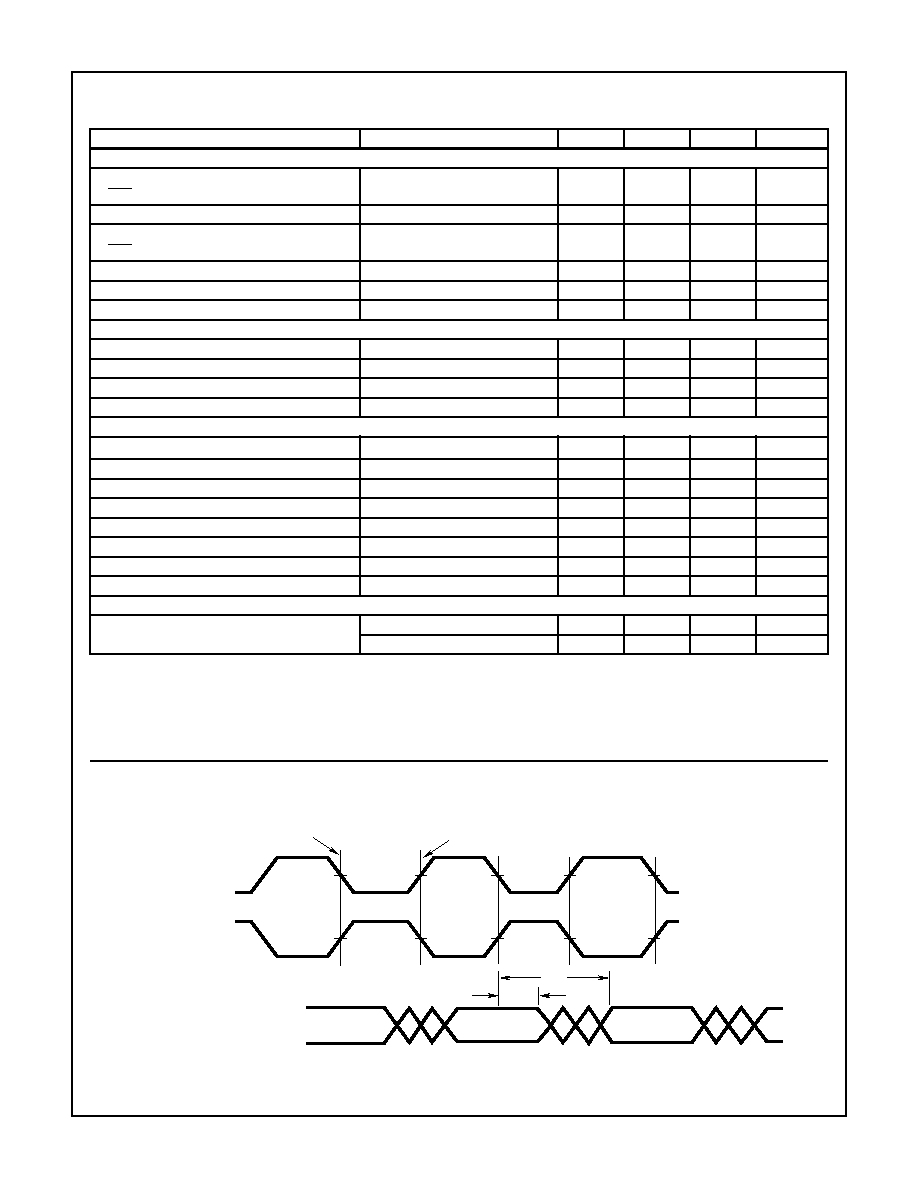
Timing Waveforms
FIGURE 1. INPUT TO OUTPUT TIMING DIAGRAM
Electrical Specifications
At 25
o
C, V
AA
+ = V
DD
= 5V, V
REF
+ = 6.4V, V
REF
- = V
AA
- = V
SS
, CLK = 15MHz,
All Reference Points Adjusted, Unless Otherwise Specified (Continued)
PARAMETER
TEST CONDITIONS
MIN
TYP
MAX
UNITS
COMPARATOR DATA IS LATCHED
DECODED DATA IS SHIFTED
TO OUTPUT REGISTERS
2
SAMPLE
N
2
1
1
2
CLOCK (PIN 18)
IF PHASE (PIN 19)
IS LOW
CLOCK IF
PHASE IS HIGH
AUTO
BALANCE
SAMPLE
N + 1
t
D
t
H
DATA
N - 2
AUTO
BALANCE
SAMPLE
N + 2
DATA
N - 1
DATA
N
CA3318

4-13
FIGURE 2. OUTPUT ENABLE TIMING DIAGRAM
FIGURE 3A. STANDBY IN INDEFINITE AUTO BALANCE (SHOWN WITH PHASE = LOW)
FIGURE 3B. STANDBY IN SAMPLE (SHOWN WITH PHASE = LOW)
FIGURE 3. PULSE MODE OPERATION
Timing Waveforms
(Continued)
t
DIS
t
EN
HIGH
IMPEDANCE
DATA
CE1
CE2
BITS 1 - 8
OF
t
DIS
t
EN
HIGH
IMPEDANCE
DATA
DATA
DATA
HIGH
IMPEDANCE
CLOCK
DATA
AUTO
BALANCE
NO MAX
LIMIT
25ns
MIN
33ns
MIN
25ns
MIN
50ns
MIN
AUTO
BALANCE
SAMPLE
N
SAMPLE
N + 1
500ns
33ns
MIN
25ns
MIN
50ns
TYP
AUTO
BALANCE
SAMPLE
N + 2
AUTO
BALANCE
SAMPLE
N + 1
SAMPLE
N
MAX
DATA
CLOCK
DATA
N - 1
DATA
N
CA3318