 | –≠–ª–µ–∫—Ç—Ä–æ–Ω–Ω—ã–π –∫–æ–º–ø–æ–Ω–µ–Ω—Ç: CD4047 | –°–∫–∞—á–∞—Ç—å:  PDF PDF  ZIP ZIP |
7-897
CAUTION: These devices are sensitive to electrostatic discharge; follow proper IC Handling Procedures.
1-888-INTERSIL or 321-724-7143 | Copyright © Intersil Corporation 1999
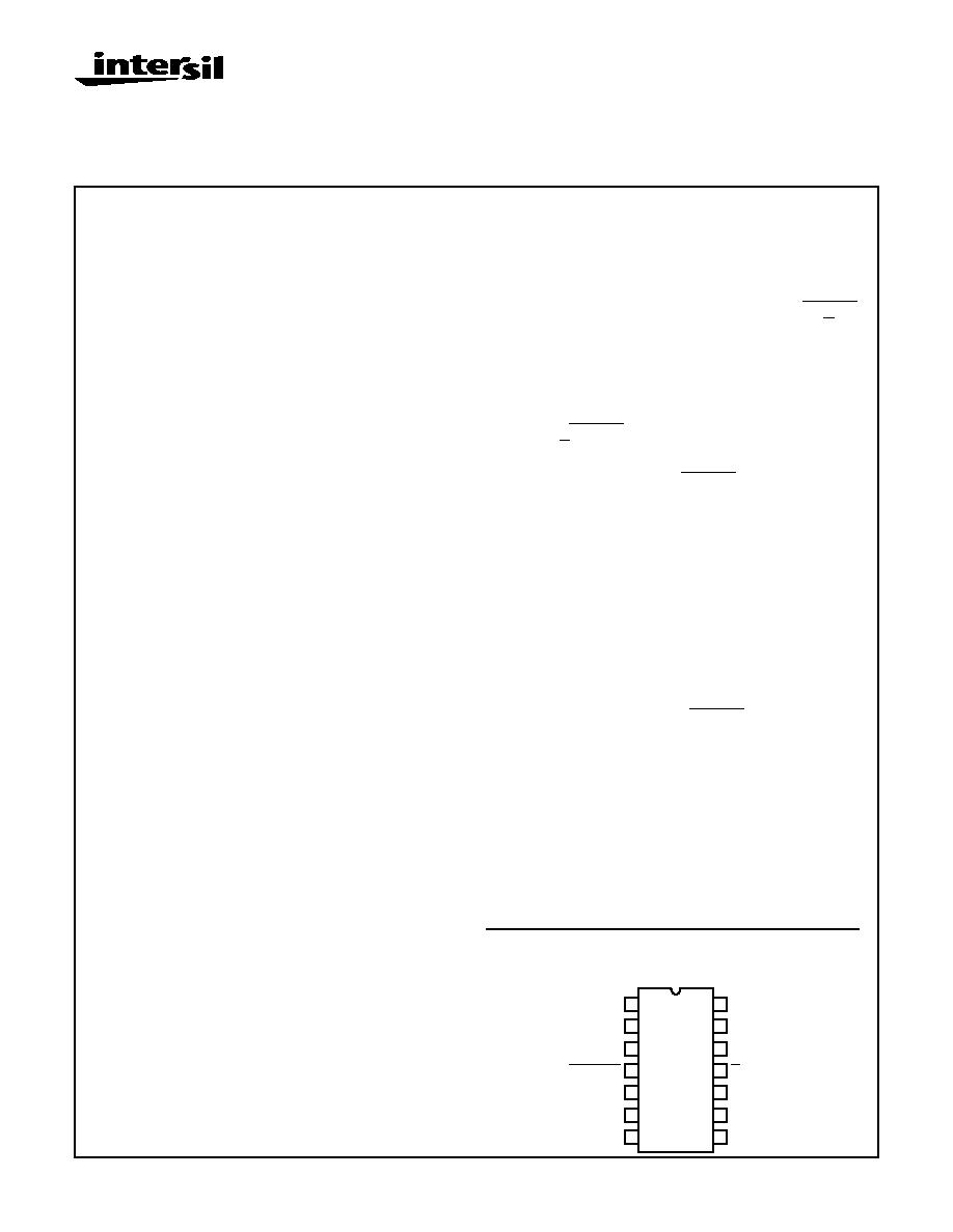
CD4047BMS
CMOS Low-Power
Monostable/Astable Multivibrator
Description
CD4047BMS consists of a gatable astable multivibrator with logic tech-
niques incorporated to permit positive or negative edge triggered
monostable multivibrator action with retriggering and external counting
options.
Inputs include +TRIGGER, -TRIGGER, ASTABLE, ASTABLE,
RETRIGGER, and EXTERNAL RESET. Buffered outputs are Q, Q, and
OSCILLATOR. In all modes of operation, an external capacitor must be
connected between C-Timing and RC-Common terminals, and an
external resistor must be connected between the R-Timing and RC-
Common terminals.
Astable operation is enabled by a high level on the ASTABLE input or a
low level on the ASTABLE input, or both. The period of the square wave
at the Q and Q Outputs in this mode of operation is a function of the
external components employed. "True" input pulses on the ASTABLE
input or "Complement" pulses on the ASTABLE input allow the circuit to
be used as a gatable multivibrator. The OSCILLATOR output period will
be half of the Q terminal output in the astable mode. However, a 50%
duty cycle is not guaranteed at this output.
The CD4047BMS triggers in the monostable mode when a positive
going edge occurs on the +TRIGGER input while the -TRIGGER is held
low. Input pulses may be of any duration relative to the output pulse.
If retrigger capability is desired, the RETRIGGER input is pulsed. The
retriggerable mode of operation is limited to positive going edge. The
CD4047BMS will retrigger as long as the RETRIGGER input is high,
with or without transitions (See Figure 31)
An external countdown option can be implemented by coupling "Q" to
an external "N" counter and resetting the counter with trigger pulse. The
counter output pulse is fed back to the ASTABLE input and has a dura-
tion equal to N times the period of the multivibrator.
A high level on the EXTERNAL RESET input assures no output pulse
during an "ON" power condition. This input can also be activated to ter-
minate the output pulse at any time. For monostable operation, when-
ever VDD is applied, an internal power on reset circuit will clock the Q
output low within one output period (tM).
The CD4047BMS is supplied in these 14-lead outline packages:
Pinout
CD4047BMS
TOP VIEW
Braze Seal DIP
H4Q
Frit Seal DIP
H1B
Ceramic Flatpack
H3W
C
R
R-C COMMON
ASTABLE
ASTABLE
-TRIGGER
VSS
VDD
OSC OUT
RETRIGGER
Q
Q
EXT. RESET
+TRIGGER
1
2
3
4
5
6
7
14
13
12
11
10
9
8
Features
∑ High Voltage Type (20V Rating)
∑ Low Power Consumption: Special CMOS Oscillator
Configuration
∑ Monostable (One-Shot) or Astable (Free-Running)
Operation
∑ True and Complemented Buffered Outputs
∑ Only One External R and C Required
∑ Buffered Inputs
∑ 100% Tested for Quiescent Current at 20V
∑ Standardized, Symmetrical Output Characteristics
∑ 5V, 10V and 15V Parametric Ratings
∑ Meets All Requirements of JEDEC Tentative Standard
No. 13B, "Standard Specifications for Description of
`B' Series CMOS Devices"
Monostable Multivibrator Features
∑ Positive or Negative Edge Trigger
∑ Output Pulse Width Independent of Trigger Pulse
Duration
∑ Retriggerable Option for Pulse Width Expansion
∑ Internal Power-On Reset Circuit
∑ Long Pulse Widths Possible Using Small RC Compo-
nents by Means of External Counter Provision
∑ Fast Recovery Time Essentially Independent of Pulse
Width
∑ Pulse-Width Accuracy Maintained at Duty Cycles
Approaching 100%
Astable Multivibrator Features
∑ Free-Running or Gatable Operating Modes
∑ 50% Duty Cycle
∑ Oscillator Output Available
∑ Good Astable Frequency Stability: Frequency Deviation:
- =
±
2% + 0.03%/
o
C at 100kHz
- =
±
0.5% + 0.015%/
o
C at 10kHz (Circuits "Trimmed"
to Frequency VDD = 10V
±
10%
Applications
Digital equipment where low power dissipation and/or high noise
immunity are primary design requirements
∑ Envelope Detection
∑ Frequency Multiplication
∑ Frequency Division
∑ Frequency Discriminators
∑ Timing Circuits
∑ Time Delay Applications
December 1992
File Number
3313
7-898
Specifications CD4047BMS
Absolute Maximum Ratings
Reliability Information
DC Supply Voltage Range, (VDD) . . . . . . . . . . . . . . . -0.5V to +20V
(Voltage Referenced to VSS Terminals)
Input Voltage Range, All Inputs . . . . . . . . . . . . .-0.5V to VDD +0.5V
DC Input Current, Any One Input
. . . . . . . . . . . . . . . . . . . . . . . .±
10mA
Operating Temperature Range . . . . . . . . . . . . . . . . -55
o
C to +125
o
C
Package Types D, F, K, H
Storage Temperature Range (TSTG) . . . . . . . . . . . -65
o
C to +150
o
C
Lead Temperature (During Soldering) . . . . . . . . . . . . . . . . . +265
o
C
At Distance 1/16
±
1/32 Inch (1.59mm
±
0.79mm) from case for
10s Maximum
Thermal Resistance . . . . . . . . . . . . . . . .
ja
jc
Ceramic DIP and FRIT Package . . . . .
80
o
C/W
20
o
C/W
Flatpack Package . . . . . . . . . . . . . . . .
70
o
C/W
20
o
C/W
Maximum Package Power Dissipation (PD) at +125
o
C
For TA = -55
o
C to +100
o
C (Package Type D, F, K) . . . . . . 500mW
For TA = +100
o
C to +125
o
C (Package Type D, F, K) . . . . . Derate
Linearity at 12mW/
o
C to 200mW
Device Dissipation per Output Transistor . . . . . . . . . . . . . . . 100mW
For TA = Full Package Temperature Range (All Package Types)
Junction Temperature . . . . . . . . . . . . . . . . . . . . . . . . . . . . . . +175
o
C
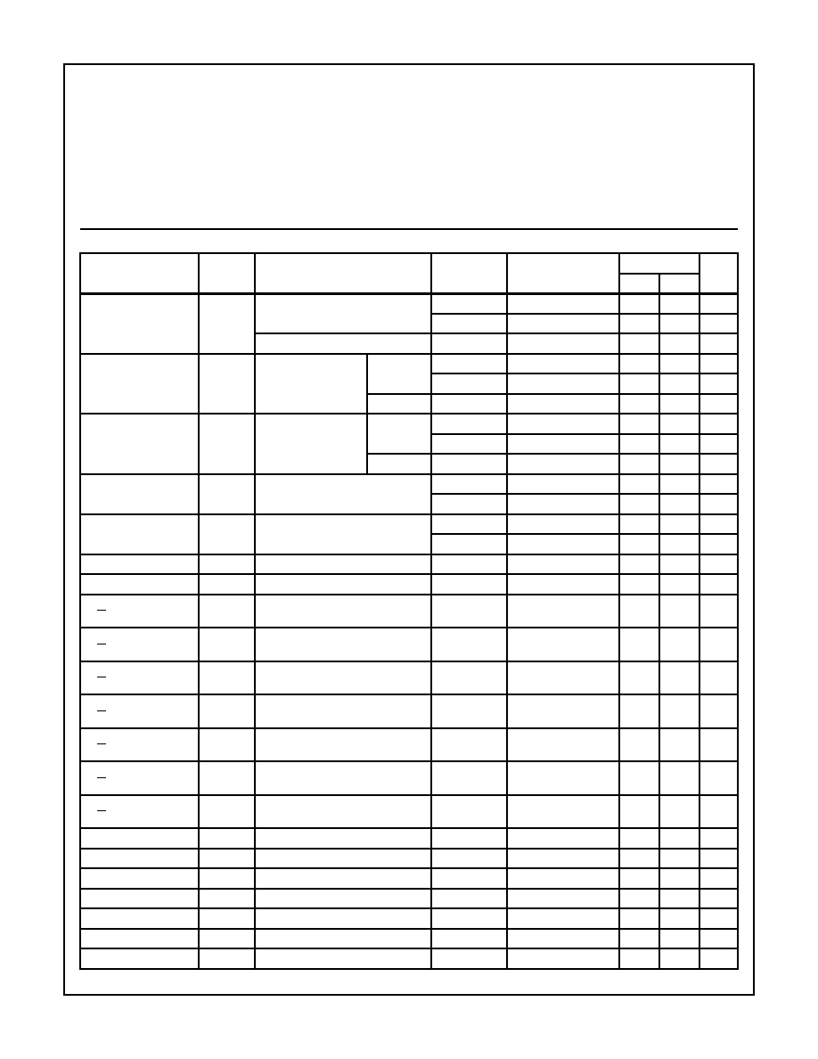
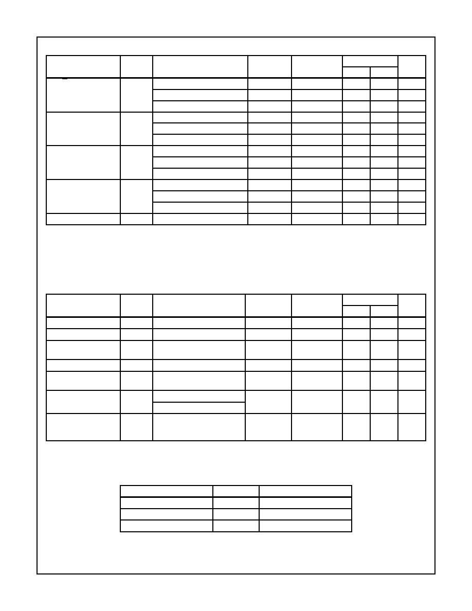
TABLE 1. DC ELECTRICAL PERFORMANCE CHARACTERISTICS
PARAMETER
SYMBOL
CONDITIONS (NOTE 1)
GROUP A
SUBGROUPS
TEMPERATURE
LIMITS
UNITS
MIN
MAX
Supply Current
IDD
VDD = 20V, VIN = VDD or GND
1
+25
o
C
-
2
µ
A
2
+125
o
C
-
200
µ
A
VDD = 18V, VIN = VDD or GND
3
-55
o
C
-
2
µ
A
Input Leakage Current
IIL
VIN = VDD or GND
VDD = 20
1
+25
o
C
-100
-
nA
2
+125
o
C
-1000
-
nA
VDD = 18V
3
-55
o
C
-100
-
nA
Input Leakage Current
IIH
VIN = VDD or GND
VDD = 20
1
+25
o
C
-
100
nA
2
+125
o
C
-
1000
nA
VDD = 18V
3
-55
o
C
-
100
nA
Input Leakage Curent
(Pin 3)
IIL
VDD = 24V, VIN = 11V or GND
1
+25
o
C
-300
-
nA
2
+125
o
C
-10
-
µ
A
Input Leakage Current
(Pin 3)
IIH
VDD = 26V, VIN = 13V or GND
1
+25
o
C
-
300
nA
2
+125
o
C
-
10
µ
A
Output Voltage
VOL15
VDD = 15V, No Load
1, 2, 3
+25
o
C, +125
o
C, -55
o
C
-
50
mV
Output Voltage
VOH15
VDD = 15V, No Load (Note 3)
1, 2, 3
+25
o
C, +125
o
C, -55
o
C 14.95
-
V
Output Current (Sink)
Q, Q, OSC Out
IOL5
VDD = 5V, VOUT = 0.4V
1
+25
o
C
0.53
-
mA
Output Current (Sink)
Q, Q, OSC Out
IOL10
VDD = 10V, VOUT = 0.5V
1
+25
o
C
1.4
-
mA
Output Current (Sink)
Q, Q, OSC Out
IOL15
VDD = 15V, VOUT = 1.5V
1
+25
o
C
3.5
-
mA
Output Current (Source)
Q, Q, OSC Out
IOH5A
VDD = 5V, VOUT = 4.6V
1
+25
o
C
-
-0.53
mA
Output Current (Source)
Q, Q, OSC Out
IOH5B
VDD = 5V, VOUT = 2.5V
1
+25
o
C
-
-1.8
mA
Output Current (Source)
Q, Q, OSC Out
IOH10
VDD = 10V, VOUT = 9.5V
1
+25
o
C
-
-1.4
mA
Output Current (Source)
Q, Q, OSC Out
IOH15
VDD = 15V, VOUT = 13.5V
1
+25
o
C
-
-3.5
mA
Output Current (Sink)
IOL5RC
VDD = 5V, VOUT = 0.4V
1
+25
o
C
0.78
-
mA
Output Current (Sink)
IOL10RC VDD = 10V, VOUT = 0.5V
1
+25
o
C
2.0
-
mA
Output Current (Sink)
IOL15RC VDD = 15V, VOUT = 1.5V
1
+25
o
C
5.2
-
mA
Output Current (Source)
IOH5RC
VDD = 5V, VOUT = 4.6V
1
+25
o
C
-
-0.78
mA
Output Current (Source) IOH10RC VDD = 10V, VOUT = 9.5V
1
+25
o
C
-
-2
mA
Output Current (Source) IOH15RC VDD = 15V, VOUT = 13.5V
1
+25
o
C
-
-5.2
mA
N Threshold Voltage
VNTH
VDD = 10V, ISS = -10
µ
A
1
+25
o
C
-2.8
-0.7
V
7-899
Specifications CD4047BMS
P Threshold Voltage
VPTH
VSS = 0V, IDD = 10
µ
A
1
+25
o
C
0.7
2.8
V
Functional
F
VDD = 2.8V, VIN = VDD or GND
7
+25
o
C
VOH >
VDD/2
VOL <
VDD/2
V
VDD = 20V, VIN = VDD or GND
7
+25
o
C
VDD = 18V, VIN = VDD or GND
8A
+125
o
C
VDD = 3V, VIN = VDD or GND
8B
-55
o
C
Input Voltage Low
(Note 2)
VIL
VDD = 5V, VOH > 4.5V, VOL < 0.5V
1, 2, 3
+25
o
C, +125
o
C, -55
o
C
-
1.5
V
Input Voltage High
(Note 2)
VIH
VDD = 5V, VOH > 4.5V, VOL < 0.5V
1, 2, 3
+25
o
C, +125
o
C, -55
o
C
3.5
-
V
Input Voltage Low
(Note 2)
VIL
VDD = 15V, VOH > 13.5V,
VOL < 1.5V
1, 2, 3
+25
o
C, +125
o
C, -55
o
C
-
4
V
Input Voltage High
(Note 2)
VIH
VDD = 15V, VOH > 13.5V,
VOL < 1.5V
1, 2, 3
+25
o
C, +125
o
C, -55
o
C
11
-
V
NOTES:
1. All voltages referenced to device GND, 100% testing being implemented
2. Go/No Go test with limits applied to inputs.
3. For accuracy, voltage is measured differentially to VDD. Limit is 0.050V max..
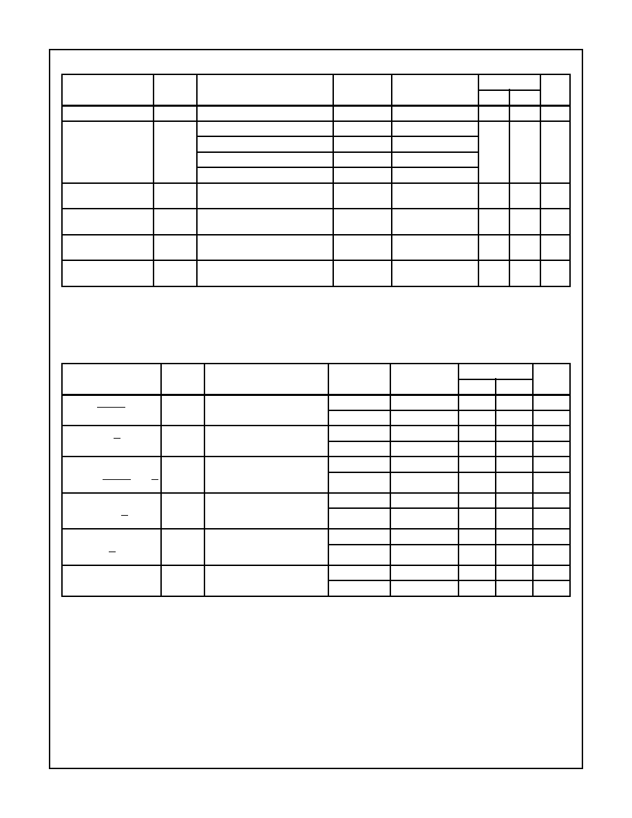
TABLE 2. AC ELECTRICAL PERFORMANCE CHARACTERISTICS
PARAMETER
SYMBOL
(NOTES 1, 2)
CONDITIONS
GROUP A
SUBGROUPS
TEMPERATURE
LIMITS
UNITS
MIN
MAX
Propagation Delay
Astable, Astable to OSC
TPLH1
VDD = 5V, VIN = VDD or GND
9
+25
o
C
-
400
ns
10, 11
+125
o
C, -55
o
C
-
540
ns
Propagation Delay
Trigger to Q, Q
TPHL3
TPLH3
VDD = 5V, VIN = VDD or GND
9
+25
o
C
-
1000
ns
10, 11
+125
o
C, -55
o
C
-
1350
ns
Propagation Delay
(Note 2)
Astable or Astable to Q, Q
TPLH2
TPLH2
VDD = 5V, VIN = VDD or GND
9
+25
o
C
-
700
ns
10, 11
+125
o
C, -55
o
C
-
945
ns
Propagation Delay
(Note 2)
Retrigger to Q, Q
TPHL4
TPLH4
VDD = 5V, VIN = VDD or GND
9
+25
o
C
-
600
ns
10, 11
+125
o
C, -55
o
C
-
810
ns
Propagation Delay
(Note 2)
Reset to Q, Q
TPLH5
TPLH5
VDD = 5V, VIN = VDD or GND
9
+25
o
C
-
500
ns
10, 11
+125
o
C, -55
o
C
-
675
ns
Transition Time
TTHL
TTLH
VDD = 5V, VIN = VDD or GND
9
+25
o
C
-
200
ns
10, 11
+125
o
C, -55
o
C
-
270
ns
NOTES:
1. VDD = 5V, CL = 50pF, RL = 200K; input TR, TF < 20ns.
2. -55
o
C and +125
o
C limits guaranteed, 100% testing being implemented.
TABLE 1. DC ELECTRICAL PERFORMANCE CHARACTERISTICS
(Continued)
PARAMETER
SYMBOL
CONDITIONS (NOTE 1)
GROUP A
SUBGROUPS
TEMPERATURE
LIMITS
UNITS
MIN
MAX
7-900
Specifications CD4047BMS
TABLE 3. ELECTRICAL PERFORMANCE CHARACTERISTICS
PARAMETER
SYMBOL
CONDITIONS
NOTES
TEMPERATURE
LIMITS
UNITS
MIN
MAX
Supply Current
IDD
VDD = 5V, VIN = VDD or GND
1, 2
-55
o
C, +25
o
C
-
1
µ
A
+125
o
C
-
30
µ
A
VDD = 10V, VIN = VDD or GND
1, 2
-55
o
C, +25
o
C
-
2
µ
A
+125
o
C
-
60
µ
A
VDD = 15V, VIN = VDD or GND
1, 2
-55
o
C, +25
o
C
-
2
µ
A
+125
o
C
-
120
µ
A
Output Voltage
VOL
VDD = 5V, No Load
1, 2
+25
o
C, +125
o
C,
-55
o
C
-
50
mV
Output Voltage
VOL
VDD = 10V, No Load
1, 2
+25
o
C, +125
o
C,
-55
o
C
-
50
mV
Output Voltage
VOH
VDD = 5V, No Load
1, 2
+25
o
C, +125
o
C,
-55
o
C
4.95
-
V
Output Voltage
VOH
VDD = 10V, No Load
1, 2
+25
o
C, +125
o
C,
-55
o
C
9.95
-
V
Output Current (Sink)
IOL5
VDD = 5V, VOUT = 0.4V
1, 2
+125
o
C
0.36
-
mA
-55
o
C
0.64
-
mA
Output Current (Sink)
IOL10
VDD = 10V, VOUT = 0.5V
1, 2
+125
o
C
0.9
-
mA
-55
o
C
1.6
-
mA
Output Current (Sink)
IOL15
VDD = 15V, VOUT = 1.5V
1, 2
+125
o
C
2.4
-
mA
-55
o
C
4.2
-
mA
Output Current (Source)
IOH5A
VDD = 5V, VOUT = 4.6V
1, 2
+125
o
C
-
-0.36
mA
-55
o
C
-
-0.64
mA
Output Current (Source)
IOH5B
VDD = 5V, VOUT = 2.5V
1, 2
+125
o
C
-
-1.15
mA
-55
o
C
-
-2.0
mA
Output Current (Source)
IOH10
VDD = 10V, VOUT = 9.5V
1, 2
+125
o
C
-
-0.9
mA
-55
o
C
-
-1.6
mA
Output Current (Source)
IOH15
VDD =15V, VOUT = 13.5V
1, 2
+125
o
C
-
-2.4
mA
-55
o
C
-
-4.2
mA
Input Voltage Low
VIL
VDD = 10V, VOH > 9V, VOL < 1V
1, 2
+25
o
C, +125
o
C,
-55
o
C
-
3
V
Input Voltage High
VIH
VDD = 10V, VOH > 9V, VOL < 1V
1, 2
+25
o
C, +125
o
C,
-55
o
C
+7
-
V
Propagation Delay
Astable, Astable to OSC
TPLH1
VDD = 10V
1, 2, 3
+25
o
C
-
200
ns
VDD = 15V
1, 2, 3
+25
o
C
-
160
ns
Propagation Delay
Astable or Astable to Q, Q
TPLH2
TPHL2
VDD = 10V
1, 2, 3
+25
o
C
-
350
ns
VDD = 15V
1, 2, 3
+25
o
C
-
250
ns
Propagation Delay
Trigger to Q, Q
TPHL3
TPLH3
VDD = 10V
1, 2, 3
+25
o
C
-
450
ns
VDD = 15V
1, 2, 3
+25
o
C
-
300
ns
Propagation Delay
Retrigger to Q, Q
TPHL4
TPLH4
VDD = 10V
1, 2, 3
+25
o
C
-
300
ns
VDD = 15V
1, 2, 3
+25
o
C
-
200
ns
Propagation Delay
Reset to Q, Q
TPLH5
TPLH5
VDD = 10V
1, 2, 3
+25
o
C
-
200
ns
VDD = 15V
1, 2, 3
+25
o
C
-
140
ns
Transition Time
TTHL
TTLH
VDD = 10V
1, 2, 3
+25
o
C
-
100
ns
VDD = 15V
1, 2, 3
+25
o
C
-
80
ns
7-901
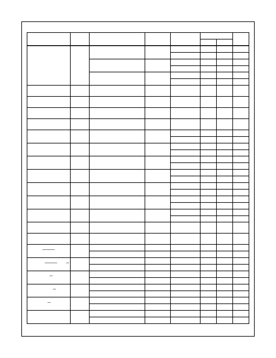
Specifications CD4047BMS
Q or Q Deviation from
50% Duty Factor
QD
VDD = 5V
1, 2, 3
+25
o
C
-
±
1
%
VDD = 10V
1, 2, 3
+25
o
C
-
±
1
%
VDD = 15V
1, 2, 3
+25
o
C
-
±
0.5
%
Minimum Pulse Width
+ Trigger
- Trigger
TW
VDD = 5V
1, 2, 3
+25
o
C
-
400
ns
VDD = 10V
1, 2, 3
+25
o
C
-
160
ns
VDD = 15V
1, 2, 3
+25
o
C
-
100
ns
Minimum Pulse Width
Reset
TW
VDD = 5V
1, 2, 3
+25
o
C
-
200
ns
VDD = 10V
1, 2, 3
+25
o
C
-
100
ns
VDD = 15V
1, 2, 3
+25
o
C
-
60
ns
Minimum Retrigger Pulse
Width
TW
VDD = 5V
1, 2, 3
+25
o
C
-
600
ns
VDD = 10V
1, 2, 3
+25
o
C
-
230
ns
VDD = 15V
1, 2, 3
+25
o
C
-
150
ns
Input Capacitance
CIN
Any Input
1, 2
+25
o
C
-
7.7
pF
NOTES:
1. All voltages referenced to device GND.
2. The parameters listed on Table 3 are controlled via design or process and are not directly tested. These parameters are characterized
on initial design release and upon design changes which would affect these characteristics.
3. CL = 50pF, RL = 200K, Input TR, TF < 20ns.
TABLE 4. POST IRRADIATION ELECTRICAL PERFORMANCE CHARACTERISTICS
PARAMETER
SYMBOL
CONDITIONS
NOTES
TEMPERATURE
LIMITS
UNITS
MIN
MAX
Supply Current
IDD
VDD = 20V, VIN = VDD or GND
1, 4
+25
o
C
-
7.5
µ
A
N Threshold Voltage
VNTH
VDD = 10V, ISS = -10
µ
A
1, 4
+25
o
C
-2.8
-0.2
V
N Threshold Voltage
Delta
VTN
VDD = 10V, ISS = -10
µ
A
1, 4
+25
o
C
-
±
1
V
P Threshold Voltage
VTP
VSS = 0V, IDD = 10
µ
A
1, 4
+25
o
C
0.2
2.8
V
P Threshold Voltage
Delta
VTP
VSS = 0V, IDD = 10
µ
A
1, 4
+25
o
C
-
±
1
V
Functional
F
VDD = 18V, VIN = VDD or GND
1
+25
o
C
VOH >
VDD/2
VOL <
VDD/2
V
VDD = 3V, VIN = VDD or GND
Propagation Delay Time
TPHL
TPLH
VDD = 5V
1, 2, 3, 4
+25
o
C
-
1.35 x
+25
o
C
Limit
ns
NOTES: 1. All voltages referenced to device GND.
2. CL = 50pF, RL = 200K, Input TR, TF < 20ns.
3. See Table 2 for +25
o
C limit.
4. Read and Record
TABLE 5. BURN-IN AND LIFE TEST DELTA PARAMETERS +25
O
C
PARAMETER
SYMBOL
DELTA LIMIT
Supply Current - MSI-1
IDD
±
0.2
µ
A
Output Current (Sink)
IOL5
±
20% x Pre-Test Reading
Output Current (Source)
IOH5A
±
20% x Pre-Test Reading
TABLE 3. ELECTRICAL PERFORMANCE CHARACTERISTICS
(Continued)
PARAMETER
SYMBOL
CONDITIONS
NOTES
TEMPERATURE
LIMITS
UNITS
MIN
MAX