
3-30
March 1997
CDP1802AC/3
High-Reliability CMOS 8-Bit Microprocessor
Features
∑ For Use In Aerospace, Military, and Critical Industrial
Equipment
∑ Minimum Instruction Fetch
-
Execute Time of 4.5
µ
s
(Maximum Clock Frequency of 3.6MHz) at V
DD
= 5V, T
A
= +25
o
C
∑ Operation Over the Full Military
Temperature Range . . . . . . . . . . . . . . . -55
o
C to +125
o
C
∑ Any Combination of Standard RAM and ROM Up to
65,536 Bytes
∑ 8≠Bit Parallel Organization With Bidirectional Data
Bus and Multiplexed Address Bus
∑ 16 x 16 Matrix of Registers for Use as Multiple Pro-
gram Counters, Data Pointers, or Data Registers
∑ On-Chip DMA, Interrupt, and Flag Inputs
∑ High Noise Immunity . . . . . . . . . . . . . . . . . . 30% of V
DD
Description
The CDP1802A/3 High
-
Reliability LSI CMOS 8
-
bit register
oriented Central
-
Processing Unit (CPU) is designed for use
as a general purpose computing or control element in a wide
range of stored
-
program systems or products.
The CDP1802A/3 includes all of the circuits required for
fetching, interpreting, and executing instructions which have
been stored in standard types of memories. Extensive
input/output (I/O) control features are also provided to facili-
tate system design.
The 1800 Series Architecture is designed with emphasis on
the total microcomputer system as an integral entity so that
systems having maximum flexibility and minimum cost can be
realized. The 1800 Series CPU also provides a synchronous
interface to memories and external controllers for I/O devices,
and minimizes the cost of interface controllers. Further, the I/O
interface is capable of supporting devices operating in polled,
interrupt
-
driven, or direct memory
-
access modes.
The CDP1802AC/3 is functionally identical to its predeces-
sor, the CDP1802. The "A" version includes some perfor-
mance enhancements and can be used as a direct
replacement in systems using the CDP1802.
This type is supplied in 40 lead dual
-
in
-
line sidebrazed
ceramic packages (D suffix).
Pinout
CDP1802AC/3 (SBDIP)
TOP VIEW
Ordering Information
PACKAGE
TEMP. RANGE
(
o
C)
5V - 3.2MHz
PKG
NO.
SBDIP
-55 to 125
CDP1802ACD3
D40.6
13
1
2
3
4
5
6
7
8
9
10
11
12
14
15
16
17
18
19
20
CLOCK
WAIT
CLEAR
Q
SC1
SC0
MRD
BUS 7
BUS 6
BUS 5
BUS 4
BUS 3
BUS 2
BUS 1
BUS 0
V
CC
N2
N1
N0
V
SS
28
40
39
38
37
36
35
34
33
32
31
30
29
27
26
25
24
23
22
21
V
DD
XTAL
DMA IN
DMA OUT
INTERRUPT
MWR
TPA
TPB
MA7
MA6
MA5
MA4
MA3
MA2
MA1
MA0
EF1
EF2
EF3
EF4
File Number
1441.2
CAUTION: These devices are sensitive to electrostatic discharge; follow proper IC Handling Procedures.
http://www.intersil.com or 407-727-9207
|
Copyright
©
Intersil Corporation 1999
[ /Title
(CDP1
802AC
/3)
/Sub-
ject
(High-
Reli-
ability
CMOS
8-Bit
Micro-
proces-
sor)
/Autho
r ()
/Key-
words
(Inter-
sil
Corpo-
ration,
8-bit
micro-
proces-
sors, 8
bit
micro-
proces-
sors,
periph-
erals)
/Cre-
ator ()
/DOCI
NFO
pdf-
mark
3-31
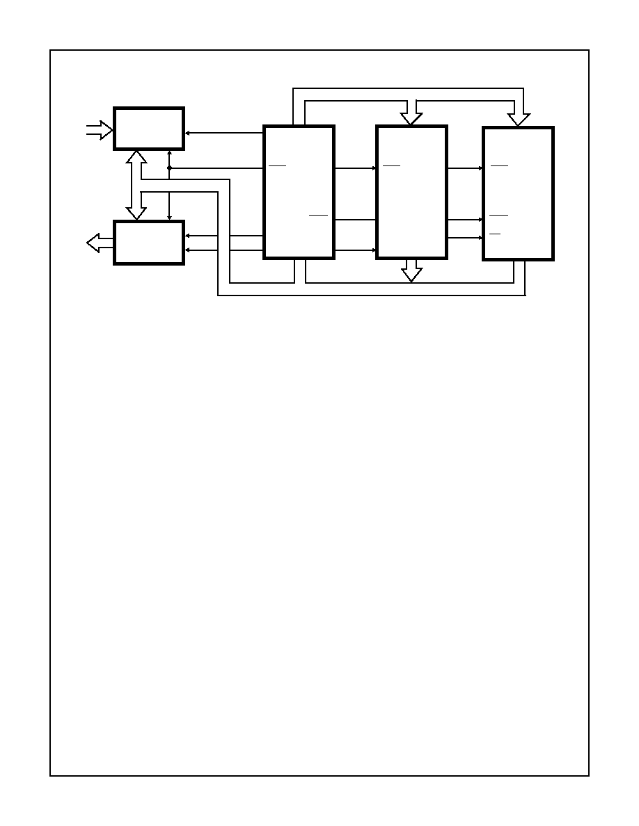
CDP1852
INPUT PORT
DATA
CS1
CS2
CDP1852
OUTPUT
PORT
CLOCK
CS1
CS2
MA0≠7
N0
MRD
MWR
N1
TPB DATA TPA
CDP1802
8≠BIT CPU
MRD
MA0≠4
MWR
CS
CDP1824
32 BYTE RAM
MA0≠7
DATA
CEO
TPA
MRD
8≠BIT DATA BUS
ADDRESS BUS
CDP1833
1K≠ROM
DATA
FIGURE 1. TYPICAL CDP1802A/3 SMALL MICROPROCESSOR SYSTEM
CDP1802AC/3

3-32
Absolute Maximum Ratings
Thermal Information
DC Supply Voltage Range, (V
DD
)
(All Voltages Referenced to V
SS
Terminal)
CDP1802AC/3 . . . . . . . . . . . . . . . . . . . . . . . . . . . . . . -0.5V to +7V
Input Voltage Range, All Inputs . . . . . . . . . . . . . -0.5V to V
DD
+0.5V
DC Input Current, any One Input
. . . . . . . . . . . . . . . . . . . . . . . . .±
10mA
Thermal Resistance (Typical)
JA
(
o
C/W)
JC
(
o
C/W)
SBDIP Package. . . . . . . . . . . . . . . . . . . .
55
15
Device Dissipation Per Output Transistor
T
A
= Full Package Temperature Range . . . . . . . . . . . . . . . . . 100mW
Operating Temperature Range (T
A
)
Package Type D. . . . . . . . . . . . . . . . . . . . . . . . . .-55
o
C to +125
o
C
Storage Temperature Range (T
STG
). . . . . . . . . . . .-65
o
C to +150
o
C
Lead Temperature (During Soldering)
At distance 1/16
±
1/32 In. (1.59
±
0.79mm)
from case for 10s max . . . . . . . . . . . . . . . . . . . . . . . . . . . +265
o
C
CAUTION: Stresses above those listed in "Absolute Maximum Ratings" may cause permanent damage to the device. This is a stress only rating and operation
of the device at these or any other conditions above those indicated in the operational sections of this specification is not implied.
Recommended Operating Conditions
T
A
= Full Package Temperature Range. For maximum reliability, operating conditions
should be selected so that operation is always within the following ranges
PARAMETER
MIN
MAX
UNITS
DC Operating Voltage Range
4
6.5
V
Input Voltage Range
V
SS
V
DD
V
Maximum Clock Input Rise or Fall Time
-
1
µ
s
Performance Specifications
PARAMETER
V
DD
(V)
-55
o
C TO +25
o
C
+125
o
C
UNITS
Minimum Instruction Time (Note 1)
5
4.5
5.9
µ
s
Maximum DMA Transfer Rate
5
450
340
Kbytes/s
Maximum Clock Input Frequency,
Load Capacitance (C
L
) = 50pF, f
CL
5
DC-3.6
DC-2.7
MHz
NOTE:
1. Equals 2 machine cycles - one Fetch and one Execute operation for all instructions except Long Branch and Long Skip, which require 3
machine cycles - one Fetch and two Execute operations.
Static Electrical Specifications
All Limits are 100% Tested
PARAMETER
CONDITIONS
-55
o
C, +25
o
C
+125
o
C
UNITS
V
OUT
(V)
V
IN,
(V)
V
CC,
V
DD
(V)
MIN
MAX
MIN
MAX
Quiescent Device Current, I
DD
-
-
5
-
100
-
250
µ
A
Output Low Drive (Sink) Current
(Except XTAL), I
OL
0.4
0, 5
5
1.20
-
0.90
-
mA
XTAL
0.4
5
5
185
-
140
-
µ
A
Output High Drive (Source)
Current (Except XTAL), I
OH
4.6
0, 5
5
-
-0.30
-
-0.20
mA
XTAL
4.6
0
5
-
-135
-
-100
µ
A
Output Voltage Low-Level, V
OL
-
0, 5
5
-
0.1
-
0.2
V
Output Voltage High-Level, V
OH
-
0, 5
5
4.9
-
4.8
-
V
CDP1802AC/3

3-33
Input Low Voltage, V
IL
0.5, 4.5
-
5
-
1.5
-
1.5
V
Input High Voltage, V
IH
0.5, 4.5
-
5
3.5
-
3.5
-
V
Input Leakage Current, I
IN
Any
Input
0, 5
5
-
±
1
-
±
5
µ
A
Three-State Output Leakage
Current, I
OUT
0, 5
0, 5
5
-
±
1
-
±
5
µ
A
NOTE:
2. 5V level characteristics apply to Part No. CDP1802AC/3, and 5V and 10V level characteristics apply to part No. CDP1802A/3.
Timing Specifications
As a Function of T (T = 1/fCLOCK), C
L
= 50 pF
PARAMETER
V
DD
(V)
LIMITS (NOTE 3)
-55
o
C, +25
o
C
+125
o
C
UNITS
High-Order Memory-Address Byte Setup to TPA
Time, t
SU
5
2T-450
2T-580
ns
High-Order Memory-Address Byte Hold After TPA Time, t
H
5
T/2 +0
T/2 +0
ns
Low-Order Memory-Address Byte Hold After WR Time, t
H
5
T-30
T-40
ns
CPU Data to Bus Hold After WR Time, t
H
5
T-170
T-250
ns
Required Memory Access Time Address to Data, t
ACC
5
5T-300
5T-400
ns
NOTE:
3. These limits are not directly tested.
Implicit Specifications
(Note 4) T
A
= -55
o
C to +25
o
C
PARAMETER
SYMBOL
V
DD
(V)
TYPICAL
VALUES
UNITS
Typical Total Power Dissipation
Idle "00" at M(0000), C
L
= 50pF
f = 2MHz
-
5
4
mW
Effective Input Capacitance any Input
-
C
IN
-
5
pF
Effective Three-State Terminal Capacitance Data Bus
-
-
7.5
pF
Minimum Data Retention Voltage
-
V
DR
-
2.4
V
Data Retention Current
-
I
DR
2.4
10
µ
A
NOTE:
4. These specifications are not tested. Typical values are provided for guidance only.
Static Electrical Specifications
All Limits are 100% Tested (Continued)
PARAMETER
CONDITIONS
-55
o
C, +25
o
C
+125
o
C
UNITS
V
OUT
(V)
V
IN,
(V)
V
CC,
V
DD
(V)
MIN
MAX
MIN
MAX
CDP1802AC/3

3-34
Dynamic Electrical Specifications
C
L
= 50pF, Timing Measurement at 0.5 V
DD
Point
PARAMETERS
V
DD
(V)
-55
o
C TO +25
o
C
+125
o
C
UNITS
MIN
MAX
MIN
MAX
Progagation Delay Times, t
PLH
, t
PHL
Clock to TPA, TPB
5
-
275
-
370
ns
Clock-to-Memory High Address Byte, t
PLH
, t
PHL
5
-
725
-
950
ns
Clock-to-Memory Low Address Byte Valid, t
PLH
, t
PHL
5
-
340
-
425
ns
Clock to MRD, t
PLH
, t
PHL
5
-
340
-
425
ns
Clock to MWR, t
PLH
, t
PHL
5
-
275
-
370
ns
Clock to (CPU DATA to BUS) Valid, t
PLH
, t
PHL
5
-
430
-
550
ns
Clock to State Code, t
PLH
, t
PHL
5
-
440
-
550
ns
Clock to Q, t
PLH
, t
PHL
5
-
375
-
475
ns
Clock to N (0 - 2), t
PLH
, t
PHL
5
-
400
-
525
ns
Interface Timing Requirements (Note 5)
Data Bus Input Setup, t
SU
5
10
-
10
-
ns
Data Bus Input Hold, t
H
5
175
-
230
-
ns
DMA Setup, t
SU
5
10
-
10
-
ns
DMA Hold, t
H
5
200
-
270
-
ns
Interrupt Setup, t
SU
5
10
-
10
-
ns
Interrupt Hold, t
H
5
175
-
230
-
ns
WAIT Setup, t
SU
5
30
-
30
-
ns
EF1-4 Setup, t
SU
5
20
-
20
-
ns
EF1-4 Hold, t
H
5
100
-
135
-
ns
Required Pulse Width Times
CLEAR Pulse Width, t
WL
5
150
-
200
-
ns
CLOCK Pulse Width, t
WL
5
140
-
185
-
ns
NOTE:
5. Minimum input setup and hold times required by Part CDP1802AC/3.
CDP1802AC/3