 | –≠–ª–µ–∫—Ç—Ä–æ–Ω–Ω—ã–π –∫–æ–º–ø–æ–Ω–µ–Ω—Ç: CDP1854 | –°–∫–∞—á–∞—Ç—å:  PDF PDF  ZIP ZIP |
5-42
Features
∑ Two Operating Modes
- Mode 0 - Functionally Compatible with Industry
Types Such as the TR1602A and CDP6402
- Mode 1 - Interfaces Directly with CDP1800-Series
Microprocessors without Additional Components
∑ Full or Half Duplex Operation
∑ Parity, Framing and Overrun Error Detection
∑ Baud Rate
- DC to 200K Bits/s at V
DD
. . . . . . . . . . . . . . . . . . . . 5V
- DC to 400K Bits/s at V
DD
. . . . . . . . . . . . . . . . . . . . 10V
∑ Fully Programmable with Externally Selectable Word
Length (5-8 Bits), Parity Inhibit, Even/Odd Parity, and
1, 1-1/2, or 2 Stop Bits
∑ False Start Bit Detection
Description
The CDP1854A and CDP1854AC are silicon-gate CMOS
Universal Asynchronous Receiver/Transmitter (UART) cir-
cuits. They are designed to provide the necessary formatting
and control for interfacing between serial and parallel data.
For example, these UARTs can be used to interface between
a peripheral or terminal with serial I/O ports and the 8-bit
CDP1800-series microprocessor parallel data bus system.
The CDP1854A is capable of full duplex operation, i.e.,
simultaneous conversion of serial input data to parallel out-
put data and parallel input data to serial output data.
The CDP1854A UART can be programmed to operate in one
of two modes by using the mode control input. When the
input is high (MODE = 1), the CDP1854A is directly compati-
ble with the CDP1800-series microprocessor system without
additional interface circuitry. When the mode input is low
(MODE = 0), the device is functionally compatible with indus-
try standard UART's such as the TR1602A and CDP6402. It
is also pin compatible with these types, except that pin 2 is
used for the mode control input.
The CDP1854A and the CDP1854AC are functionally identi-
cal. The CDP1854A has a recommended operating voltage
range of 4V to 10.5V, and the CDP1854AC has a recom-
mended operating voltage range of 4V to 6.5V.
Ordering Information
PACKAGE
TEMP.
RANGE
5V/200K
BAUD
10V/400K
BAUD
PKG.
NO.
PDIP
-40
o
C to +85
o
C CDP1854ACE
CDP1854AE
E40.6
Burn-In
CDP1854ACEX
CDP1854AEX
E40.6
PLCC
-40
o
C to +85
o
C CDP1854ACQ
CDP1854AQ
N44.65
SBDIP
-40
o
C to +85
o
C CDP1854ACD
CDP1854AD
D40.6
Burn-In
CDP1854ACDX
-
D40.6
March 1997
CDP1854A,
CDP1854AC
Programmable Universal Asynchronous
Receiver/Transmitter (UART)
File Number
1193.2
CAUTION: These devices are sensitive to electrostatic discharge; follow proper IC Handling Procedures.
http://www.intersil.com or 407-727-9207
|
Copyright
©
Intersil Corporation 1999
5-43
Pinouts
40 LEAD SBDIP, PDIP (MODE 0)
TOP VIEW
40 LEAD SBDIP, PDIP (MODE 1)
TOP VIEW
44 LEAD PLCC (Q SUFFIX)
TOP VIEW
13
1
2
3
4
5
6
7
8
9
10
11
12
14
15
16
17
18
19
20
V
DD
MODE (V
SS
)
V
SS
RRD
R BUS 7
R BUS 6
R BUS 5
R BUS 4
R BUS 3
R BUS 2
R BUS 1
R BUS 0
PE
FE
OE
SFD
R CLOCK
DAR
DA
SDI
28
40
39
38
37
36
35
34
33
32
31
30
29
27
26
25
24
23
22
21
T CLOCK
EPE
WLS 1
WLS 2
SBS
PI
CRL
T BUS 7
T BUS 6
T BUS 5
T BUS 4
T BUS 3
T BUS 2
T BUS 1
T BUS 0
SD0
TSRE
THRL
THRE
MR
13
1
2
3
4
5
6
7
8
9
10
11
12
14
15
16
17
18
19
20
V
DD
MODE (V
DD
)
V
SS
CS2
R BUS 7
R BUS 6
R BUS 5
R BUS 4
R BUS 3
R BUS 2
R BUS 1
R BUS 0
INT
FE
PE/OE
RSEL
R CLOCK
TPB
DA
SDI
28
40
39
38
37
36
35
34
33
32
31
30
29
27
26
25
24
23
22
21
T CLOCK
CTS
ES
PS1
NC
CS3
RD/WR
T BUS 7
T BUS 6
T BUS 5
T BUS 4
T BUS 3
T BUS 2
T BUS 1
T BUS 0
SD0
RTS
CS1
THRE
CLEAR
NC = NO CONNECT
44 43 42 41 40
39
38
37
36
35
34
33
32
31
30
29
28
27
1
2
3
4
5
6
20 21 22 23 24 25 26
19
18
7
8
9
10
11
12
13
14
15
16
17
R BUS 6
R BUS 5
R BUS 4
R BUS 3
R BUS 2
NC
R BUS 1
R BUS 0
PE(INT)
FE
OE(PE/OE)
PI (CS3)
CRL(RD/WR)
T BUS 7
T BUS 6
T BUS 5
NC
T BUS 4
T BUS 3
T BUS 2
T BUS 1
T BUS 0
R B
US 7
RRD (
CS2)
V
SS
MODE
V
DD
NC
T CLOCK
EPE (
CTS)
WLS1 (
ES)
WLS2 (
PSI)
SBS (NC)
SFD (RSEL)
R CLOCK
(TPB)
D
AR
DA
(
D
A)
SDI
NC
MR(
CLEAR)
THRE(
THRE)
THRL(CS1)
TSRE(
R
TS)
SD0
NOTE:
MODE 0(MODE 1)
CDP1854A, CDP1854AC
5-44
Block Diagram
Mode Input High (Mode = 1)
NOTE: 1. User Interconnect
FIGURE 1. MODE 1 BLOCK DIAGRAM (CDP1800-SERIES MICROPROCESSOR COMPATIBLE)
SELECT
LOGIC
23
4
35
CS1
CS2
CS3
INT
13
INT
STATUS
REGISTER
22
14
15
THRE
FE
PE/OE
19
D
A
CONTROL
REG
TRANSMITTER
HOLDING
REGISTER
TRANSMITTER BUS
(26 - 33)
(SEE NOTE 1)
TRANSMITTER
SHIFT
REGISTER
PARITY
GEN
THREE-STATE
DRIVERS
RECEIVER BUS
(5-12)
(SEE NOTE 1)
(SEE NOTE 1)
MUX
TRANSMITTER
TIMING &
CONTROL
40
24
39
T CLOCK
R
TS
CTS
TRANSMITTER SECTION
RECEIVER
TIMING &
CONTROL
38
37
17
ES
PSI
R CLOCK
RECEIVER SECTION
RECEIVER
HOLDING
REGISTER
SHIFT
REGISTER
CDP1802
INTERFACE
34
18
16
RD/
WR
TPB
RSEL
20
SDI
25
SDO
1, 2 = V
DD
3 = V
SS
21 = CLEAR
36 = NC
CDP1854A, CDP1854AC
5-45
Absolute Maximum Ratings
Thermal Information
DC Supply-Voltage Range, (V
DD
)
(Voltages Referenced to V
SS
Terminal)
CDP1854A . . . . . . . . . . . . . . . . . . . . . . . . . . . . . . . . .-0.5 to +11V
CDP1854AC . . . . . . . . . . . . . . . . . . . . . . . . . . . . . . . . .-0.5 to +7V
Input Voltage Range, All Inputs . . . . . . . . . . . . . .-0.5 to V
DD
+ 0.5V
DC Input Current, Any One Input
. . . . . . . . . . . . . . . . . . . . . . . . .±
10mA
Device Dissipation Per Output Transistor
T
A
= Full Package-Temperature Range . . . . . . . . . . . . . . 100mW
Operating-Temperature Range (T
A
)
Package Type D . . . . . . . . . . . . . . . . . . . . . . . . . -55
o
C to +125
o
C
Package Type E and Q . . . . . . . . . . . . . . . . . . . . . -40
o
C to +85
o
C
Thermal Resistance (Typical, Note 1)
JA
(
o
C/W)
JC
(
o
C/W)
SBDIP Package . . . . . . . . . . . . . . . . . .
55
15
PDIP Package . . . . . . . . . . . . . . . . . . .
50
N/A
PLCC Package . . . . . . . . . . . . . . . . . .
46
N/A
Maximum Junction Temperature
Plastic Package . . . . . . . . . . . . . . . . . . . . . . . . . . . . . . . . . +150
o
C
Ceramic Package . . . . . . . . . . . . . . . . . . . . . . . . . . . . . . . +175
o
C
Maximum Storage Temperature Range (T
STG
) . . .-65
o
C to +150
o
C
Maximum Lead Temperature (Soldering 10s):
At Distance 1/16
±
1/32 inch (1.59
±
0.79mm) . . . . . . . . . . +265
o
C
NOTE: Printed circuit board mount: 57mm x 57mm minimum area x
1.6mm thick G10 epoxy glass, or equivalent.
CAUTION: Stresses above those listed in "Absolute Maximum Ratings" may cause permanent damage to the device. This is a stress only rating and operation of
the device at these or any other conditions above those indicated in the operational sections of this specification is not implied.
NOTE:
1.
JA
is measured with the component mounted on an evaluation PC board in free air.
Static Electrical Specifications
at T
A
= -40
o
C to +85
o
C, Unless Otherwise Noted
PARAMETER
CONDITIONS
LIMITS
UNITS
V
O
(V)
V
IN
(V)
V
DD
(V)
CDP1854A
CDP1854AC
MIN
(NOTE 1)
TYP
MAX
MIN
(NOTE 1)
TYP
MAX
Quiescent Device
Current
I
DD
-
0, 5
5
-
0.01
50
-
0.02
200
µ
A
-
0, 10
10
-
1
200
-
-
-
µ
A
Output Low Drive
(Sink) Current
(Except pins 24 and
25)
I
OL
0.4
0, 5
5
1
2
-
1
2
-
mA
0.5
0, 10
10
2
4
-
-
-
-
mA
Output High Drive
(Source) Current
I
OH
4.6
0, 5
5
-0.55
-1.1
-
-0.55
-1.1
-
mA
9.5
0, 10
10
-1.3
-2.6
-
-
-
-
mA
Output Low Drive
(Sink) Current
(Pins 24 and 25)
I
OL
0.4
0, 5
5
1.6
3.5
-
1.6
3.5
-
mA
0.5
0, 10
10
3.2
7
-
-
-
-
mA
Output Voltage
Low-Level (Note 2)
V
OL
-
0, 5
5
-
0
0.1
-
0
0.1
V
-
0, 10
10
-
0
0.1
-
-
-
V
Output Voltage
High-Level (Note 2)
V
OH
-
0, 5
5
4.9
5
-
4.9
5
-
V
-
0, 10
10
9.9
10
-
-
-
-
V
Input Low Voltage
V
IL
0.5, 4.5
-
5
-
-
1.5
-
-
1.5
V
0.5, 9.5
-
10
-
-
3
-
-
-
V
Input High Voltage
V
IH
0.5, 4.5
-
5
3.5
-
-
3.5
-
-
V
0.5, 9.5
-
10
7
-
-
-
-
-
V
Input Current
I
IN
-
0, 5
5
-
-
±
1
-
-
±
1
µ
A
-
0, 10
10
-
-
±
2
-
-
-
µ
A
CDP1854A, CDP1854AC
5-46
Three-State Output
Leakage Current
I
OUT
0, 5
0, 5
5
-
-
±
1
-
-
±
1
µ
A
0, 10
0, 10
10
-
-
±
10
-
-
-
µ
A
Operating Current
(Note 3)
I
DD1
-
0, 5
5
-
1.5
-
-
1.5
-
mA
-
0, 10
10
-
6
-
-
-
-
mA
Input Capacitance
C
IN
-
-
-
-
5
7.5
-
5
7.5
pF
Output Capacitance
C
OUT
-
-
-
-
10
15
-
10
15
pF
NOTES:
1. Typical values are for T
A
= 25
o
C.
2. I
OL
= I
OH
= 1
µ
A.
3. Operating current is measured at 200kHz or V
DD
= 5V and 400kHz for V
DD
= 10V in a CDP1800-series microprocessor system, with
open outputs.
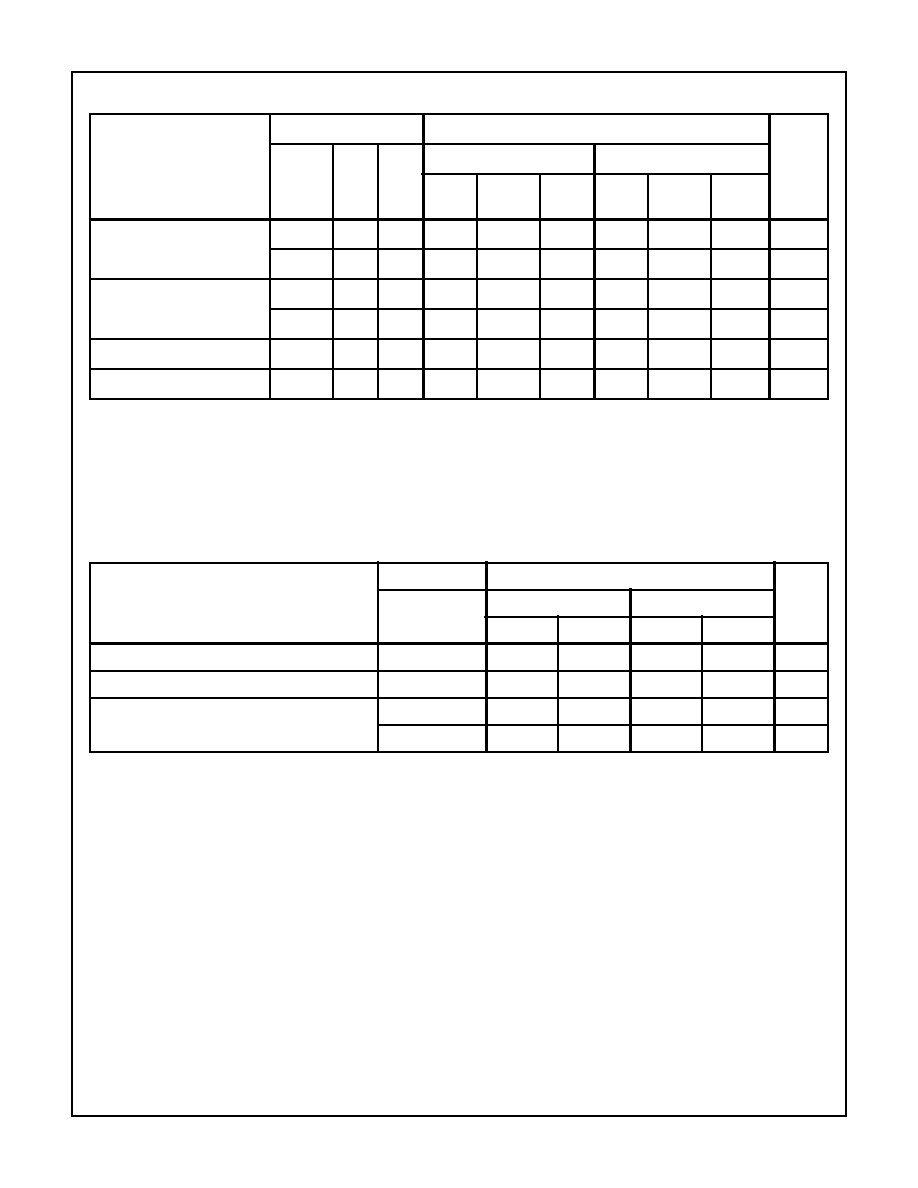
Operating Conditions
At T
A
= Full Package-Temperature Range. For maximum reliability, operating conditions should be selected so
that operation is always within the following ranges:
PARAMETER
CONDITIONS
LIMITS
UNITS
V
DD
(V)
CDP1854A
CDP1854AC
MIN
MAX
MIN
MAX
DC Operating Voltage Range
-
4
10.5
4
6.5
V
Input Voltage Range
-
V
SS
V
DD
V
SS
V
DD
V
Baud Rate (Receive or Transmit)
5
-
200
-
200
K bits/s
10
-
400
-
-
K bits/s
Static Electrical Specifications
at T
A
= -40
o
C to +85
o
C, Unless Otherwise Noted (Continued)
PARAMETER
CONDITIONS
LIMITS
UNITS
V
O
(V)
V
IN
(V)
V
DD
(V)
CDP1854A
CDP1854AC
MIN
(NOTE 1)
TYP
MAX
MIN
(NOTE 1)
TYP
MAX
CDP1854A, CDP1854AC