 | –≠–ª–µ–∫—Ç—Ä–æ–Ω–Ω—ã–π –∫–æ–º–ø–æ–Ω–µ–Ω—Ç: CDP1882 | –°–∫–∞—á–∞—Ç—å:  PDF PDF  ZIP ZIP |

4-1
CDP1881C,
CDP1882, CDP1882C
CMOS 6-Bit Latch
and Decoder Memory Interfaces
Features
∑ Performs Memory Address Latch and Decoder
Functions Multiplexed or Non-Multiplexed
∑ Decodes Up to 16K Bytes of Memory
∑ Interfaces Directly with CDP1800-Series Microproces-
sors at Maximum Clock Frequency
∑ Can Replace CDP1866 and CDP1867 (Upward Speed
and Function Capability)
Ordering Information
Description
The CDP1881C, CDP1882 and CDP1882C are CMOS 6-bit
memory latch and decoder circuits intended for use in
CDP1800 series microprocessor systems. They can inter-
face directly with the multiplexed address bus of this system
at maximum clock frequency, and up to four 4K x 8-bit mem-
ories to provide a 16K byte memory system. With four 2K x
8-bit memories an 8K byte system can be decoded.
The devices are also compatible with non-multiplexed
address bus microprocessors. By connecting the clock input
to V
DD
, the latches are in the data-following mode and the
decoded outputs can be used in general purpose memory-
system applications.
The CDP1881C, CDP1882 and CDP1882C are intended for
use with 2K or 4K byte RAMs and are identical except that in
the CDP1882 MWR and MRD are excluded.
The CDP1882 is functionally identical to the CDP1882C. It
differs in that the CDP1882 has recommended operating
voltage range of 4V to 10.5V and the C version has a recom-
mended operating voltage range of 4V to 6.5V.
The CDP1881C, CDP1882 and CDP1882C are supplied in
20 lead and 18 lead packages, respectively. The
CDP1881C is supplied only in a dual-in-line plastic pack-
age (E suffix). The CDP1882 is supplied in dual-in-line,
hermetic side-brazed ceramic (D suffix) and in plastic (E
suffix) packages.
Pinouts
CDP1881C
(PDIP)
TOP VIEW
CDP1882, CDP1882C
(PDIP, CERDIP)
TOP VIEW
PACKAGE
5V
10V
TEMP.
RANGE
(
o
C)
PKG.
NO.
PDIP
CDP1881CE
-
-40 to +85
E20.3
PDIP
CDP1882CE
-
-40 to +85
E18.3
PDIP
Burn-In
CDP1882CEX
-
-40 to +85
E18.3
SBDIP
-
CDP1882D
-40 to +85
D18.3
11
12
13
14
15
16
17
18
20
19
10
9
8
7
6
5
4
3
2
1
CLOCK
MA5
MA4
MA3
MA2
MA1
MRD
MA0
MWR
V
SS
V
DD
A9
A10
A11
A8
CS0
CS1
CS2
CS3
CE
10
11
12
13
14
15
16
17
18
9
8
7
6
5
4
3
2
1
V
DD
A9
A10
A11
CS0
CS1
CS2
A8
CS3
CLOCK
MA5
MA4
MA3
MA2
MA1
CE
MA0
V
SS
File Number
1367.2
March 1997
CAUTION: These devices are sensitive to electrostatic discharge; follow proper IC Handling Procedures.
http://www.intersil.com or 407-727-9207
|
Copyright
©
Intersil Corporation 1999

4-2
Absolute Maximum Ratings
Thermal Information
DC Supply Voltage Range, (V
DD
)
(All Voltages Referenced to V
SS
Terminal)
CDP1882 . . . . . . . . . . . . . . . . . . . . . . . . . . . . . . . . -0.5V to +11V
CDP1881C and CDP1882C. . . . . . . . . . . . . . . . . . . -0.5V to +7V
Input Voltage Range, All Inputs . . . . . . . . . . . . . -0.5V to V
DD
+0.5V
DC Input Current, Any One Input
. . . . . . . . . . . . . . . . . . . . . . . . .±
10mA
Thermal Resistance (Typical)
JA
(
o
C/W)
JC
(
o
C/W)
18 Lead PDIP . . . . . . . . . . . . . . . . . . .
85
N/A
20 Lead PDIP . . . . . . . . . . . . . . . . . . .
80
N/A
SBDIP Package . . . . . . . . . . . . . . . . . .
85
22
Device Dissipation Per Output Transistor
T
A
= Full Package Temperature Range
(All Package Types) . . . . . . . . . . . . . . . . . . . . . . . . . . . . . . 100mW
Operating Temperature Range (T
A
)
Package Type D. . . . . . . . . . . . . . . . . . . . . . . . . . -55
o
C to +125
o
C
Package Type E . . . . . . . . . . . . . . . . . . . . . . . . . . . -40
o
C to +85
o
C
Storage Temperature Range (T
STG
) . . . . . . . . . . . . -65
o
C to +150
o
C
Lead Temperature (During Soldering)
At distance 1/16
±
1/32 In. (1.59
±
0.79mm)
from case for 10s max . . . . . . . . . . . . . . . . . . . . . . . . . . . . +265
o
C
CAUTION: Stresses above those listed in the "Absolute Maximum Ratings" may cause permanent damage to the device. This is a stress only rating and opera-
tion of the device at these or any other conditions above those indicated in the operation section of this specification is not implied.
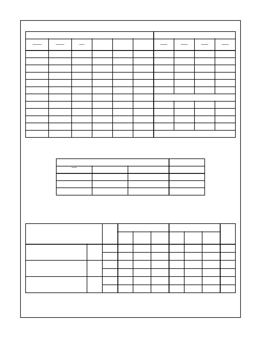
Recommended Operating Conditions
At T
A
= Full Package Temperature Range. For maximum reliability, operating conditions
should be selected so that operation is always within the following ranges:
PARAMETER
CDP1882
CDP1881C, CDP1882C
UNITS
MIN
MAX
MIN
MAX
DC Operating Voltage Range
4
10.5
4
6.5
V
Input Voltage Range
V
SS
V
DD
V
SS
V
DD
V
Static Electrical Specifications
At T
A
= -40
o
C to +85
o
C, V
DD
±
5%, Except as Noted:
PARAMETER
SYMBOL
CONDITIONS
CDP1882
CDP1881C, CDP1882C
UNITS
V
O
(V)
V
IN
(V)
V
DD
(V)
MIN
(NOTE 1)
TYP
MAX
MIN
(NOTE 1)
TYP
MAX
Quiescent Device
Current
I
DD
-
0, 5
5
-
1
10
-
5
50
µ
A
-
0, 10
10
-
10
100
-
-
-
µ
A
Output Low Drive
(Sink) Current
I
OL
0.4
0, 5
5
1.6
3.2
-
1.6
3.2
-
mA
0.5
0, 10
10
3.2
6.4
-
-
-
-
mA
Output High Drive
(Source) Current
I
OH
4.6
0, 5
5
-1.15
-2.3
-
-1.15
-2.3
-
mA
9.5
0, 10
10
-2.3
-4.6
-
-
-
-
mA
Output Voltage
Low-Level (Note 2)
V
OL
-
0, 5
5
-
0
0.1
-
0
0.1
V
-
0, 10
10
-
0
0.1
-
-
-
V
Output Voltage
High-Level (Note 2)
V
OH
-
0, 5
5
4.9
5
-
4.9
5
-
V
-
0, 10
10
9.9
10
-
-
-
-
V
Input Low Voltage
V
IL
0.5, 4.5
-
5
-
-
1.5
-
-
1.5
V
1, 9
-
10
-
-
3
-
-
-
V
Input High Voltage
V
IH
0.5, 9.5
-
5
3.5
-
-
3.5
-
-
V
1, 9
-
10
7
-
-
-
-
-
V
CDP1881C, CDP1882, CDP1882C

4-3
Input Leakage Current
I
IN
Any
Input
0, 5
5
-
-
±
1
-
-
±
1
µ
A
0, 10
10
-
-
±
2
-
-
-
µ
A
Operating Current
(Note 2)
I
DD1
0, 5
0, 5
5
-
-
2
-
-
2
mA
0, 10
0, 10
10
-
-
4
-
-
-
mA
Input Capacitance
C
IN
-
-
-
-
5
7.5
-
5
7.5
pF
Output Capacitance
C
OUT
-
-
-
-
10
15
-
10
15
pF
Minimum Data
Retention Voltage
V
DR
V
DD
= V
DR
-
2
2.4
-
2
2.4
V
Data Retention Current
I
DR
V
DD
= 2.4V
-
0.01
1
-
0.5
5
µ
A
NOTES:
1. Typical values are for T
A
= +25
o
C.
2. I
OL
= I
OH
= 1
µ
A.
3. Operating current measured at 200kHz for V
DD
= 5V and 400kHz for V
DD
= 10V, with outputs open circuits (equivalent to typical CDP1800
system at 3.2MHz, 5V; and 6.4MHz, 10V).
FIGURE 1. FUNCTIONAL DIAGRAM FOR THE CDP1881C
FIGURE 2. FUNCTIONAL DIAGRAM FOR THE CDP1882,
CDP1882C
Static Electrical Specifications
At T
A
= -40
o
C to +85
o
C, V
DD
±
5%, Except as Noted: (Continued)
PARAMETER
SYMBOL
CONDITIONS
CDP1882
CDP1881C, CDP1882C
UNITS
V
O
(V)
V
IN
(V)
V
DD
(V)
MIN
(NOTE 1)
TYP
MAX
MIN
(NOTE 1)
TYP
MAX
19
18
17
16
15
14
13
12
20
10
D
C
Q
D
C
Q
D
C
Q
D
C
Q
D
C
Q
Q
D
C
Q
Q
7
6
5
4
3
2
1
8
9
11
MA0
MA1
MA2
MA3
MA4
MA5
CLOCK
MRD
MWR
CE
A8
A9
A10
A11
CS0
CS1
CS2
CS3
V
DD
=
V
SS
=
17
16
15
14
13
12
11
10
18
9
D
C
Q
D
C
Q
D
C
Q
D
C
Q
D
C
Q
Q
D
C
Q
Q
7
6
5
4
3
2
1
8
MA0
MA1
MA2
MA3
MA4
MA5
CLOCK
CE
A8
A9
A10
A11
CS0
CS1
CS2
CS3
V
DD
=
V
SS
=
CDP1881C, CDP1882, CDP1882C
4-4
TRUTH TABLE
INPUTS
OUTPUTS
(NOTE 1)
MWR
(NOTE 1)
MRD
CE
CLK
MA4
MA5
CS0
CS1
CS2
CS3
1
1
X
X
X
X
1
1
1
1
X
X
1
X
X
X
1
1
1
1
0
X
0
1
0
0
0
1
1
1
0
X
0
1
1
0
1
0
1
1
0
X
0
1
0
1
1
1
0
1
0
X
0
1
1
1
1
1
1
0
0
X
0
0
X
X
Previous State
X
0
0
1
0
0
0
1
1
1
X
0
0
1
1
0
1
0
1
1
X
0
0
1
0
1
1
1
0
1
X
0
0
1
1
1
1
1
1
0
X
0
0
0
X
X
Previous State
NOTE:
1. CDP1881C Only
INPUTS
OUTPUTS
CE
CLK
MA0, MA1, MA2, MA3
A8, A9, A10, A11
X
1
1
1
X
1
0
0
X
0
X
Previous State
Logic 1 = High, Logic 0 = Low, X = Don't Care
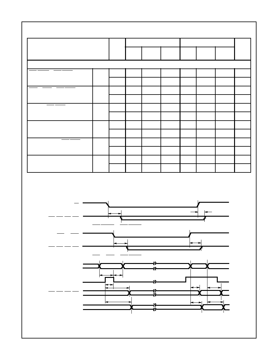
Dynamic Electrical Specifications
at T
A
= -40
o
C to +85
o
C, V
DD
±
5%, t
R
, t
F
= 20ns, V
IH
= 0.7 V
DD
, V
IL
= 0.3 V
DD
, C
L
= 100pF,
(See Figure 1)
PARAMETER
V
DD
(V)
CDP1882
CDP1881C, CDP1882C
UNITS
MIN
(NOTE 1)
TYP
(NOTE 2)
MAX
MIN
(NOTE 1)
TYP
(NOTE 2)
MAX
Minimum Setup Time
t
MACL
5
-
10
35
-
10
35
ns
Memory Address to CLOCK
10
-
8
25
-
-
-
ns
Minimum Hold Time
t
CLMA
5
-
8
25
-
8
25
ns
Memory Address After CLOCK
10
-
8
25
-
-
-
ns
Minimum CLOCK Pulse Width
t
CLCL
5
-
50
75
-
50
75
ns
10
-
25
40
-
-
-
ns
CDP1881C, CDP1882, CDP1882C
4-5
PROPAGATION DELAY TIMES
Chip Enable to Chip Select
t
CECS
5
-
75
150
-
75
150
ns
10
-
45
100
-
-
-
ns
MRD or MRW to Chip Select (Note 3)
t
MCS
5
-
75
150
-
75
150
ns
10
-
40
100
-
-
-
ns
CLOCK to Chip Select
t
CLCS
5
-
100
175
-
100
175
ns
10
-
65
125
-
-
-
ns
CLOCK to Address
t
CLA
5
-
100
175
-
100
175
ns
10
-
65
125
-
-
-
ns
Memory Address to Chip Select
t
MACS
5
-
100
175
-
100
175
ns
10
-
75
125
-
-
-
ns
Memory Address to Address
t
MAA
5
-
80
125
-
80
125
ns
10
-
40
60
-
-
-
ns
NOTES:
1. Typical values are for T
A
= 25
o
C.
2. Maximum limits of minimum characteristics are the values above which all devices function.
3. For CDP1881C type only.
Dynamic Electrical Specifications
at T
A
= -40
o
C to +85
o
C, V
DD
±
5%, t
R
, t
F
= 20ns, V
IH
= 0.7 V
DD
, V
IL
= 0.3 V
DD
, C
L
= 100pF,
(See Figure 1) (Continued)
PARAMETER
V
DD
(V)
CDP1882
CDP1881C, CDP1882C
UNITS
MIN
(NOTE 1)
TYP
(NOTE 2)
MAX
MIN
(NOTE 1)
TYP
(NOTE 2)
MAX
FIGURE 3. TIMING WAVEFORMS
CE
CS0, CS1, CS2, CS3
MRD OR MWR
CS0, CS1, CS2, CS3
MA0 - MA5
CLOCK
A8 - A11
VALID CHIP ENABLE
t
CECS
(A) CHIP ENABLE TO CHIP SELECT PROPAGATION DELAY
(B) MRD OR MWR TO CHIP SELECT PROPAGATION DELAY (CDP1881C ONLY)
t
MCS
t
MACL
t
CLMA
t
CLCL
t
CLCS
t
CLA
(C) MEMORY ADDRESS SETUP AND HOLD TIME
t
CECS
t
MCS
t
MACS
t
MACS
t
MAA
t
MAA
CS0, CS1, CS2, CS3
CDP1881C, CDP1882, CDP1882C