 | –≠–ª–µ–∫—Ç—Ä–æ–Ω–Ω—ã–π –∫–æ–º–ø–æ–Ω–µ–Ω—Ç: CDP1883CE | –°–∫–∞—á–∞—Ç—å:  PDF PDF  ZIP ZIP |
4-129
CDP1883,
CDP1883C
CMOS 7-Bit Latch
and Decoder Memory Interfaces
March 1997
Features
∑ Performs Memory Address Latch and Decoder Func-
tions Multiplexed or Non-Multiplexed
∑ Interfaces Directly with the CDP1800-Series Micropro-
cessors
∑ Allows Decoding for Systems Up to 32K Bytes
Description
The CDP1883 is a CMOS 7-bit memory latch and decoder
circuit intended for use in CDP1800-series microprocessor
systems. It can serve as a direct interface between the multi-
plexed address bus of this system and up to four 8K x 8-bit
memories to implement a 32K-byte memory system. With
four 4K x 8-bit memories, a 16K-byte system can be
decoded.
The device is also compatible with non-multiplexed address
bus microprocessors. By connecting the clock input to V
DD
,
the latches are in the data-following mode and the decoded
outputs can be used in general-purpose memory-system
applications.
The CDP1833 is compatible with CDP1800-series micropro-
cessors operating at maximum clock frequency.
The CDP1883 and CDP1883C are functionally identical.
They differ in that the CDP1883 has a recommended operat-
ing voltage range of 4V to 10.5V and the C version has a
recommended operating voltage range of 4V to 6.5V.
The CDP1883 and CDP1883C are supplied in 20 lead dual-
in-line plastic packages (E Suffix).
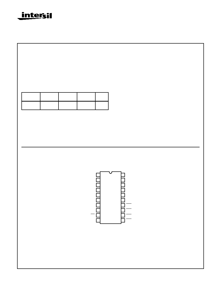
Pinout
CDP1883, CDP1883C
(PDIP)
TOP VIEW
Ordering Information
5V
10V
TEMP.
RANGE
PACKAGE
PKG.
NO.
CDP1883CE CDP1883E
-40
o
C to
+85
o
C
PDIP
E20.3
11
12
13
14
15
16
17
18
20
19
10
9
8
7
6
5
4
3
2
1
CLOCK
MA0
MA1
MA2
MA3
MA4
MA6
MA5
CE
V
SS
V
DD
A9
A10
A11
A8
A12
CS0
CS1
CS2
CS3
File Number
1507.2
CAUTION: These devices are sensitive to electrostatic discharge; follow proper IC Handling Procedures.
http://www.intersil.com or 407-727-9207
|
Copyright
©
Intersil Corporation 1999
4-130
Absolute Maximum Ratings
Thermal Information
DC Supply Voltage Range, (V
DD
)
(All Voltages Referenced to V
SS
Terminal)
CDP1883 . . . . . . . . . . . . . . . . . . . . . . . . . . . . . . . . -0.5V to +11V
CDP1883C. . . . . . . . . . . . . . . . . . . . . . . . . . . . . . . . -0.5V to +7V
Input Voltage Range, All Inputs . . . . . . . . . . . . . -0.5V to V
DD
+0.5V
DC Input Current, Any One Input
. . . . . . . . . . . . . . . . . . . . . . . . .±
10mA
Thermal Resistance (Typical)
JA
(
o
C/W)
PDIP Package . . . . . . . . . . . . . . . . . . . . . . . . . . . . .
80
Device Dissipation Per Output Transistor
T
A
= Full Package Temperature Range . . . . . . . . . . . . . . . 100mW
Operating Temperature Range (T
A
)
Package Type E . . . . . . . . . . . . . . . . . . . . . . . . . . .-40
o
C to +85
o
C
Storage Temperature Range (T
STG
). . . . . . . . . . . .-65
o
C to +150
o
C
Lead Temperature (During Soldering)
At distance 1/16
±
1/32 In. (1.59
±
0.79mm)
from case for 10s max . . . . . . . . . . . . . . . . . . . . . . . . . . . . +265
o
C
CAUTION: Stresses above those listed in the "Absolute Maximum Ratings" may cause permanent damage to the device. This is a stress only rating and opera-
tion of the device at these or any other conditions above those indicated in the operation section of this specification is not implied.
Recommended Operating Conditions
At T
A
= Full Package Temperature Range. For maximum reliability, operating conditions
should be selected so that operation is always within the following ranges:
PARAMETER
SYMBOL
CDP1883
CDP1883C
UNITS
MIN
MAX
MIN
MAX
DC Operating Voltage Range
4
10.5
4
6.5
V
Input Voltage Range
V
SS
V
DD
V
SS
V
DD
V
Static Electrical Specifications
At T
A
= -40
o
C to +85
o
C, V
DD
±
5
%,
Except as Noted:
PARAMETER
SYMBOL
CONDITIONS
CDP1883
CDP1883C
UNITS
V
O
(V)
V
IN
(V)
V
DD
(V)
MIN
(NOTE 1)
TYP
MAX
MIN
(NOTE 1)
TYP
MAX
Quiescent Device
Current
I
DD
-
0, 5
5
-
1
10
-
5
50
µ
A
-
0, 10
10
-
10
100
-
-
-
µ
A
Output Low Drive
(Sink) Current
I
OL
0.4
0, 5
5
1.6
3.2
-
1.6
3.2
-
mA
0.5
0, 10
10
3.2
6.4
-
-
-
-
mA
Output High Drive
(Source) Current
I
OH
4.6
0, 5
5
-1.15
-2.3
-
-1.15
-2.3
-
mA
9.5
0, 10
10
-2.3
-4.6
-
-
-
-
mA
Output Voltage
Low-Level (Note 2)
V
OL
-
0, 5
5
-
0
0.1
-
0
0.1
V
-
0, 10
10
-
0
0.1
-
-
-
V
Output Voltage
High-Level (Note 2)
V
OH
-
0, 5
5
4.9
5
-
4.9
5
-
V
-
0, 10
10
9.9
10
-
-
-
-
V
Input Low Voltage
V
IL
0.5, 4.5
-
5
-
-
1.5
-
-
1.5
V
0.5, 9.5
-
10
-
-
3
-
-
-
V
Input High Voltage
V
IH
0.5, 4.5
-
5
3.5
-
-
3.5
-
-
V
0.5, 9.5
-
10
7
-
-
-
-
-
V
Input Leakage Current
I
IN
Any
Input
0, 5
5
-
-
±
1
-
-
±
1
µ
A
0, 10
10
-
-
±
2
-
-
-
µ
A
Operating Current
(Note 3)
I
DD1
0, 5
0, 5
5
-
-
2
-
-
2
mA
0, 10
0, 10
10
-
-
4
-
-
-
mA
CDP1883, CDP1883C

4-131
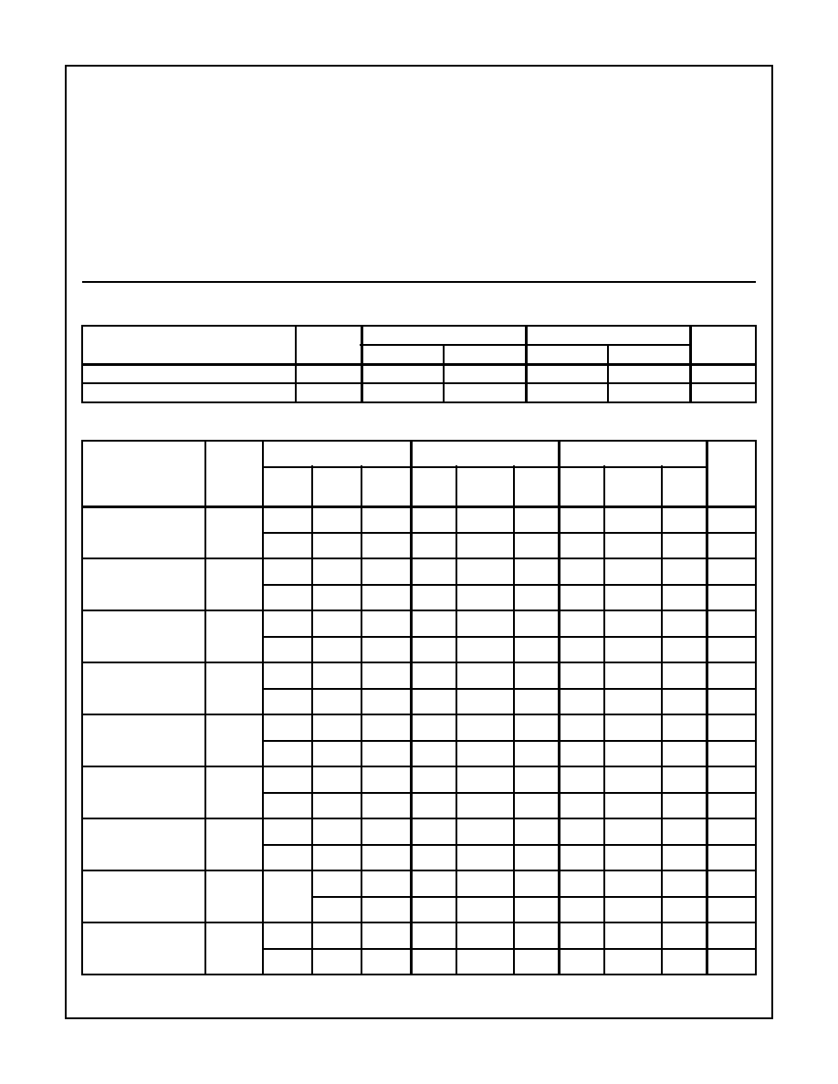
Functional Diagram
Minimum Data
Retention Voltage
V
DR
V
DD
= V
DR
-
2
2.4
-
2
2.4
V
Data Retention Current
I
DR
V
DD
= 2.4V
-
0.01
1
-
0.5
5
µ
A
Input Capacitance
C
IN
-
-
-
-
5
7.5
-
5
7.5
pF
Output Capacitance
C
OUT
-
-
-
-
10
15
-
10
15
pF
NOTES:
1. Typical values are for T
A
= +25
o
C.
2. I
OL
= I
OH
=
µ
A
3. Operating current measured at 200kHz for V
DD
= 5V and 400kHz for V
DD
= 10V, with outputs open circuit.
Static Electrical Specifications
At T
A
= -40
o
C to +85
o
C, V
DD
±
5
%,
Except as Noted: (Continued)
PARAMETER
SYMBOL
CONDITIONS
CDP1883
CDP1883C
UNITS
V
O
(V)
V
IN
(V)
V
DD
(V)
MIN
(NOTE 1)
TYP
MAX
MIN
(NOTE 1)
TYP
MAX
2
3
4
5
6
7
8
1
20
10
9
11
12
13
14
17
16
15
18
19
D
C
Q
D
C
Q
D
C
Q
D
C
Q
D
C
Q
Q
D
C
Q
D
C
Q
Q
MA0
MA1
MA2
MA3
MA4
MA5
MA6
CLOCK
CE
A8
A9
A10
A11
A12
CS0
CS1
CS2
CS3
V
DD
=
V
SS
=
CDP1883, CDP1883C

4-132
Signal Descriptions/Pin Functions
CLOCK: Latch Input Control - a high on the clock input will
allow data to pass through the latch to the output pin. Data is
latched on the high-to-low transition of the clock input. This
pin is connected to TPA in CDP1800-series systems and tied
to V
DD
for other applications.
MA0 - MA4: Address inputs to the high-byte address
latches.
MA5 - MA6: High byte address inputs decoded to produce
chip selects CS0 - CS3.
CE: CHIP ENABLE input - A low on this pin will enable the
chip select decoder. A high on this pin forces CS0, CS1,
CS2, and CS3 outputs to a high (false) state.
A8 - A12: Latched high-byte address outputs.
CS0 - CS3: One of four latched and decoded Chip Select
outputs.
V
DD
, V
SS
: Power and ground pins, respectively.
Application Information
The CDP1883 and CDP1883C can be interfaced, without
external components, with CDP1800-series microprocessor
systems. These microprocessors feature a multiplexed
address bus and provide an address latch signal (TPA) that
is used as the clock input of the CDP1883. See Figure 2 and
Figure 3.
This signal is used to latch 7 bits of the high-order address.
The lower five high-order address inputs are latched and
held to be used with the eight lower-order address inputs to
access an 8K x 8-bit memory. The two upper high-order
address inputs are latched and decoded for use as chip
selects.
The latched address and decoding functions of the
CDP1883 and CDP1883C allow them to operate with 32K-
byte memory systems. In addition, smaller memory systems
can be configured with 4K x 8-bit or smaller memories, or a
mix of memory sizes up to 8K x 8-bit.
TRUTH TABLE
INPUTS
OUTPUTS
CE
CLK
MA5
MA6
CS0
CS1
CS2
CS3
0
1
0
0
0
1
1
1
0
1
1
0
1
0
1
1
0
1
0
1
1
1
0
1
0
1
1
1
1
1
1
0
0
0
X
X
Previous State
1
X
X
X
1
1
1
1
TRUTH TABLE
INPUTS
OUTPUTS
CE
CLK
MA0 - 4
A8 - A12
X
1
1
1
X
1
0
0
X
0
X
Previous State
X = Don't Care
Dynamic Electrical Specifications
T
A
= -40
o
C to +85
o
C, V
DD
±
5%, t
R
, t
F
= 20ns, V
IH
= 0.7 V
DD
, V
IL
= 0.3 V
DD
, C
L
= 100pF.
See Figure 1
PARAMETER
V
DD
(V)
CDP1883
CDP1883C
UNITS
MIN
(NOTE 1)
TYP
(NOTE 2)
MAX
MIN
(NOTE 1)
TYP
(NOTE 2)
MAX
Minimum Setup Time,
Memory Address to CLOCK
t
MACL
5
-
10
35
-
10
35
ns
10
-
8
25
-
-
-
ns
Minimum Hold Time,
Memory Address After CLOCK
t
CLMA
5
-
8
25
-
8
25
ns
10
-
8
25
-
-
-
ns
Minimum CLOCK Pulse Width
t
CLCL
5
-
50
75
-
50
75
ns
10
-
25
40
-
-
-
ns
PROPAGATION DELAY TIMES
Chip Enable to Chip Select
t
CECS
5
-
75
150
-
75
150
ns
10
-
45
100
-
-
-
ns
CLOCK to Chip Select
t
CLCS
5
-
100
175
-
100
175
ns
10
-
65
125
-
-
-
ns
CDP1883, CDP1883C
4-133
All Intersil semiconductor products are manufactured, assembled and tested under ISO9000 quality systems certification.
Intersil products are sold by description only. Intersil Corporation reserves the right to make changes in circuit design and/or specifications at any time without
notice. Accordingly, the reader is cautioned to verify that data sheets are current before placing orders. Information furnished by Intersil is believed to be accurate
and reliable. However, no responsibility is assumed by Intersil or its subsidiaries for its use; nor for any infringements of patents or other rights of third parties which
may result from its use. No license is granted by implication or otherwise under any patent or patent rights of Intersil or its subsidiaries.
For information regarding Intersil Corporation and its products, see web site http://www.intersil.com
CLOCK to Address
t
CLA
5
-
100
175
-
100
175
ns
10
-
65
125
-
-
-
ns
Memory Address to Chip Select
t
MACS
5
-
100
175
-
100
175
ns
10
-
75
125
-
-
-
ns
Memory Address to Address
t
MAA
5
-
80
125
-
80
125
ns
10
-
40
60
-
-
-
ns
NOTES:
1. Typical values are for T
A
= 25
o
C.
2. Maximum limits of minimum characteristics are the values above which all devices function.
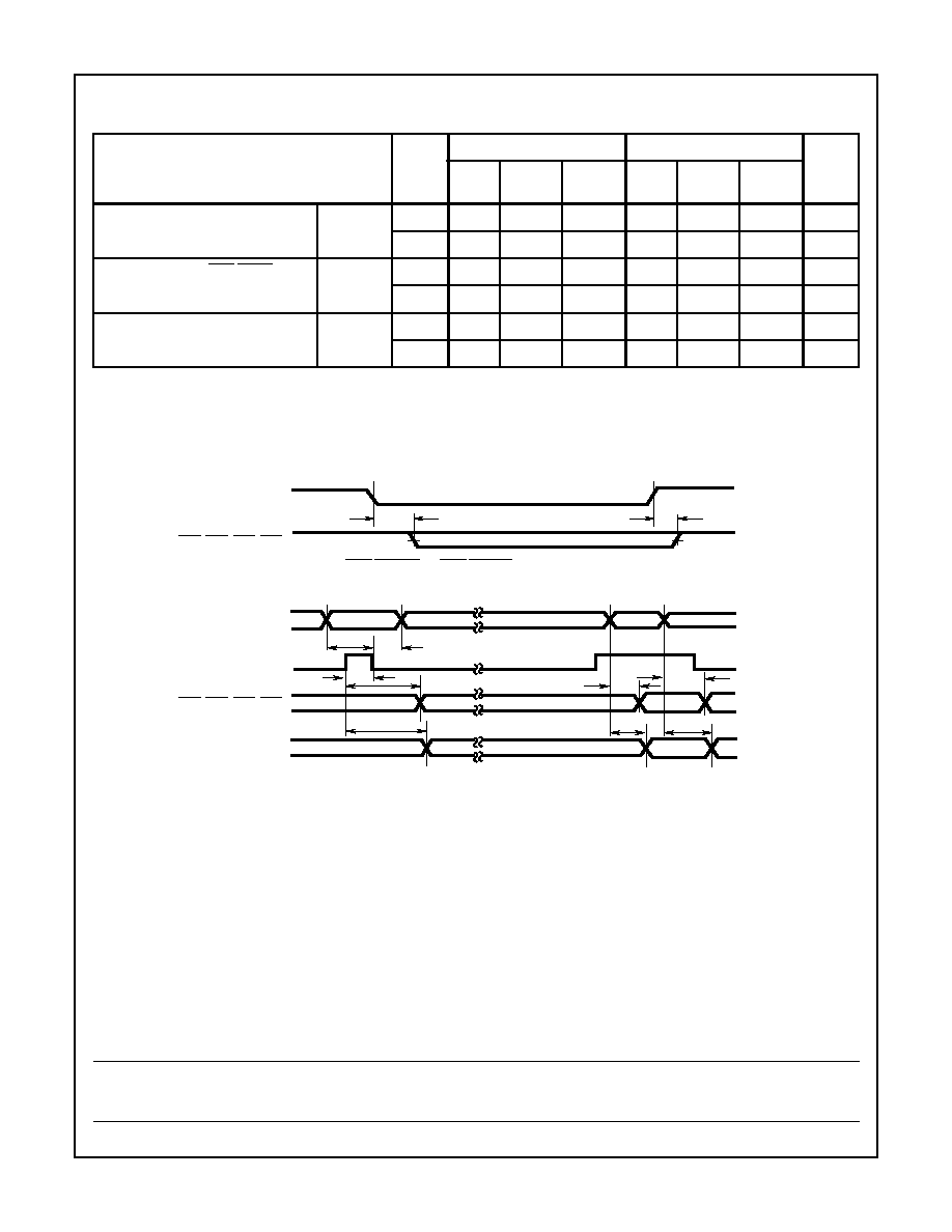
FIGURE 1. CDP1883 TIMING WAVEFORMS
Dynamic Electrical Specifications
T
A
= -40
o
C to +85
o
C, V
DD
±
5%, t
R
, t
F
= 20ns, V
IH
= 0.7 V
DD
, V
IL
= 0.3 V
DD
, C
L
= 100pF.
See Figure 1 (Continued)
PARAMETER
V
DD
(V)
CDP1883
CDP1883C
UNITS
MIN
(NOTE 1)
TYP
(NOTE 2)
MAX
MIN
(NOTE 1)
TYP
(NOTE 2)
MAX
VALID CHIP ENABLE
(A) CHIP ENABLE TO CHIP SELECT PROPAGATION DELAY
(B) MEMORY ADDRESS SETUP AND HOLD TIME
t
CECS
t
CECS
t
CLMA
t
MACL
t
CLCL
t
CLCS
t
CLA
A8 - A12
CS0, CS1, CS2, CS3
CLOCK
MA0 - MA5
CS0, CS1, CS2, CS3
CE
t
MACS
t
MACS
t
MAA
t
MAA
CDP1883, CDP1883C