Äîêóìåíòàöèÿ è îïèñàíèÿ www.docs.chipfind.ru
1
®
FN6140.1
CAUTION: These devices are sensitive to electrostatic discharge; follow proper IC Handling Procedures.
1-888-INTERSIL or 1-888-468-3774
|
Intersil (and design) is a registered trademark of Intersil Americas Inc.
Copyright Intersil Americas Inc. 2005. All Rights Reserved
All other trademarks mentioned are the property of their respective owners.
MS82C55A, MQ82C55A
CMOS Programmable Peripheral Interface
The Intersil 82C55A is a high performance CMOS version of
the industry standard 8255A and is manufactured using a
self-aligned silicon gate CMOS process (Scaled SAJI IV). It
is a general purpose programmable I/O device which may
be used with many different microprocessors. There are 24
I/O pins which may be individually programmed in two
groups of 12 and used in three major modes of operation.
The high performance and industry standard configuration of
the 82C55A make it compatible with the 80C86, 80C88 and
other microprocessors.
Static CMOS circuit design insures low operating power. The
Intersil advanced SAJI process results in performance equal
to or greater than existing functionally equivalent products at
a fraction of the power.
Features
· Pb-Free Plus Anneal Available (RoHS Compliant)
(See Ordering Info)
· Pin Compatible with OKI MSM82C55A
- No Bus Hold Devices on any Port Pins
· 24 Programmable I/O Pins
· Fully TTL Compatible
· High Speed, No "Wait State" Operation with 8MHz 80C86
and 80C88
· Direct Bit Set/Reset Capability
· Enhanced Control Word Read Capability
· L7 Process
· 2.5mA Drive Capability on All I/O Ports
· Low Standby Power (ICCSB) . . . . . . . . . . . . . . . . . . .10
µA
Ordering Information
PART
NUMBERS*
TEMP.
RANGE (°C)
PACKAGE
PKG. DWG. #
CMS82C55AZ
(Note)
0 to 70
44 Ld PLCC
(Pb-free)
N44.65
IMS82C55AZ
(Note)
-40 to 85
CMQ82C55AZ
(Note)
0 to 70
44 Ld MQFP
(Pb-free)
Q44.10x10
IMQ82C55AZ
(Note)
-40 to 85
*Add "96" suffix to part number for tape and reel packaging.
NOTE: Intersil Pb-free plus anneal products employ special Pb-free
material sets; molding compounds/die attach materials and 100%
matte tin plate termination finish, which are RoHS compliant and
compatible with both SnPb and Pb-free soldering operations. Intersil
Pb-free products are MSL classified at Pb-free peak reflow
temperatures that meet or exceed the Pb-free requirements of
IPC/JEDEC J STD-020.
Data Sheet
June 28, 2005
2
FN6140.1
June 28, 2005
Pinouts
MS82C55A (PLCC)
TOP VIEW
MQ82C55A (MQFP)
TOP VIEW
CS
GND
A1
A0
PC7
PC6
PC5
PC4
PC0
PC1
PC
3
PB
0
PB
1
PB
2
PB
3
PB
4
PB
5
PB
6
PB
7
NC
NC
RESET
D0
D1
D2
D3
D4
D5
D6
D7
V
CC
RD
PA
0
PA
1
PA
2
PA
3
PA
4
PA
5
PA
6
PA
7
WR
NC
PC
2
NC
44 43 42 41 40
39
38
37
36
35
34
33
32
31
30
29
28
27
1
2
3
4
5
6
26
25
24
23
22
21
20
19
18
7
8
9
10
11
12
13
14
15
16
17
PC6
PC7
A0
A1
GND
CS
1
2
3
4
5
6
7
8
9
10
11
12 13 14 15 16 17
PC5
PC4
PC0
PC1
PC2
28
27
26
25
24
23
22
21
20
19
18
PB7
V
CC
D7
D6
D5
D4
39 38 37 36 35 34
33
32
31
30
29
44 43 42 41 40
NC
PA
4
PA
5
PA
6
PA
7
WR
RESET
D0
D1
D2
D3
RD
PA
0
PA
1
PA
2
PA
3
NC
PB3
PB4
PB5
PB6
NC
NC
PC3
PB0
PB1
PB2
Pin Description
SYMBOL
TYPE
DESCRIPTION
V
CC
V
CC
: The +5V power supply pin. A 0.1
µF capacitor between V
CC
and GND is recommended for decoupling.
GND
GROUND
D0-D7
I/O
DATA BUS: The Data Bus lines are bidirectional three-state pins connected to the system data bus.
RESET
I
RESET: A high on this input clears the control register and all ports (A, B, C) are set to the input mode.
CS
I
CHIP SELECT: Chip select is an active low input used to enable the 82C55A onto the Data Bus for CPU
communications.
RD
I
READ: Read is an active low input control signal used by the CPU to read status information or data via the data bus.
WR
I
WRITE: Write is an active low input control signal used by the CPU to load control words and data into the 82C55A.
A0-A1
I
ADDRESS: These input signals, in conjunction with the RD and WR inputs, control the selection of one of the three
ports or the control word register. A0 and A1 are normally connected to the least significant bits of the Address Bus
A0, A1.
PA0-PA7
I/O
PORT A: 8-bit input and output port.
PB0-PB7
I/O
PORT B: 8-bit input and output port.
PC0-PC7
I/O
PORT C: 8-bit input and output port.
MS82C55A, MQ82C55A
3
FN6140.1
June 28, 2005
Functional Diagram
Functional Description
Data Bus Buffer
This three-state bidirectional 8-bit buffer is used to interface
the 82C55A to the system data bus. Data is transmitted or
received by the buffer upon execution of input or output
instructions by the CPU. Control words and status
information are also transferred through the data bus buffer.
Read/Write and Control Logic
The function of this block is to manage all of the internal and
external transfers of both Data and Control or Status words.
It accepts inputs from the CPU Address and Control busses
and in turn, issues commands to both of the Control Groups.
(CS) Chip Select. A "low" on this input pin enables the
communication between the 82C55A and the CPU.
(RD) Read. A "low" on this input pin enables 82C55A to send
the data or status information to the CPU on the data bus. In
essence, it allows the CPU to "read from" the 82C55A.
(WR) Write. A "low" on this input pin enables the CPU to
write data or control words into the 82C55A.
(A0 and A1) Port Select 0 and Port Select 1. These input
signals, in conjunction with the RD and WR inputs, control
the selection of one of the three ports or the control word
register. They are normally connected to the least significant
bits of the address bus (A0 and A1).
(RESET) Reset. A "high" on this input initializes the control
register to 9Bh and all ports (A, B, C) are set to the input
mode.
GROUP A
PORT A
(8)
GROUP A
PORT C
UPPER
(4)
GROUP B
PORT C
LOWER
(4)
GROUP B
PORT B
(8)
GROUP B
CONTROL
GROUP A
CONTROL
DATA BUS
BUFFER
READ
WRITE
CONTROL
LOGIC
RD
WR
A1
A0
RESET
CS
D7-D0
POWER
SUPPLIES
+5V
GND
BIDIRECTIONAL
DATA BUS
I/O
PA7-PA0
I/O
PC7-PC4
I/O
PC3-PC0
I/O
PB7-PB0
8-BIT
INTERNAL
DATA BUS
FIGURE 1. FUNCTIONAL DIAGRAM
82C55A BASIC OPERATION
A1
A0
RD
WR
CS
INPUT OPERATION
(READ)
0
0
0
1
0
Port A
Data Bus
0
1
0
1
0
Port B
Data Bus
1
0
0
1
0
Port C
Data Bus
1
1
0
1
0
Control Word
Data Bus
OUTPUT OPERATION
(WRITE)
0
0
1
0
0
Data Bus
Port A
0
1
1
0
0
Data Bus
Port B
1
0
1
0
0
Data Bus
Port C
1
1
1
0
0
Data Bus
Control
DISABLE FUNCTION
X
X
X
X
1
Data Bus
Three-State
X
X
1
1
0
Data Bus
Three-State
MS82C55A, MQ82C55A
4
FN6140.1
June 28, 2005
Group A and Group B Controls
The functional configuration of each port is programmed by
the systems software. In essence, the CPU "outputs" a
control word to the 82C55A. The control word contains
information such as "mode", "bit set", "bit reset", etc., that
initializes the functional configuration of the 82C55A.
Each of the Control blocks (Group A and Group B) accepts
"commands" from the Read/Write Control logic, receives
"control words" from the internal data bus and issues the
proper commands to its associated ports.
Control Group A - Port A and Port C upper (C7 - C4)
Control Group B - Port B and Port C lower (C3 - C0)
The control word register can be both written and read as
shown in the "Basic Operation" table. Figure 4 shows the
control word format for both Read and Write operations.
When the control word is read, bit D7 will always be a logic
"1", as this implies control word mode information.
Ports A, B, and C
The 82C55A contains three 8-bit ports (A, B, and C). All can
be configured to a wide variety of functional characteristics
by the system software but each has its own special features
or "personality" to further enhance the power and flexibility of
the 82C55A.
Port A One 8-bit data output latch/buffer and one 8-bit data
input latch.
Port B One 8-bit data input/output latch/buffer and one 8-bit
data input buffer.
Port C One 8-bit data output latch/buffer and one 8-bit data
input buffer (no latch for input). This port can be divided into
two 4-bit ports under the mode control. Each 4-bit port
contains a 4-bit latch and it can be used for the control signal
output and status signal inputs in conjunction with ports A
and B.
Operational Description
Mode Selection
There are three basic modes of operation than can be
selected by the system software:
Mode 0 - Basic Input/Output
Mode 1 - Strobed Input/Output
Mode 2 - Bidirectional Bus
When the reset input goes "high", all ports will be set to the
input mode. After the reset is removed, the 82C55A can
remain in the input mode with no additional initialization
required. The control word register will contain 9Bh. During
the execution of the system program, any of the other modes
may be selected using a single output instruction. This
allows a single 82C55A to service a variety of peripheral
devices with a simple software maintenance routine. Any
port programmed as an output port is initialized to all zeros
when the control word is written.
FIGURE 2. 82C55A BLOCK DIAGRAM. DATA BUS BUFFER,
READ/WRITE, GROUP A & B CONTROL LOGIC
FUNCTIONS
GROUP A
PORT A
(8)
GROUP A
PORT C
UPPER
(4)
GROUP B
PORT C
LOWER
(4)
GROUP B
PORT B
(8)
GROUP B
CONTROL
GROUP A
CONTROL
DATA
READ
WRITE
CONTROL
LOGIC
RD
WR
A1
A0
RESET
CS
D7-D0
POWER
SUPPLIES
+5V
GND
BIDIRECTIONAL
DATA BUS
I/O
PA7-
I/O
PC7-
I/O
PC3-
I/O
PB7-
BUFFER
BUS
PB0
PC0
PC4
PA0
8-BIT
INTERNAL
DATA BUS
FIGURE 3. BASIC MODE DEFINITIONS AND BUS INTERFACE
DATA BUS
8
I/O
B
PB7-PB0
4
I/O
PC3-PC0
4
I/O
C
PC7-PC4
8
I/O
A
PA7-PA0
CONTROL BUS
ADDRESS BUS
RD, WR
82C55A
D7-D0
A0-A1
CS
MODE 0
8
I/O
B
PB7-PB0
CONTROL
C
8
I/O
A
PA7-PA0
MODE 1
OR I/O
CONTROL
OR I/O
8
I/O
B
PB7-PB0
C
BI-
A
PA7-PA0
MODE 2
CONTROL
DIRECTIONAL
MS82C55A, MQ82C55A
5
FN6140.1
June 28, 2005
The modes for Port A and Port B can be separately defined,
while Port C is divided into two portions as required by the
Port A and Port B definitions. All of the output registers,
including the status flip-flops, will be reset whenever the
mode is changed. Modes may be combined so that their
functional definition can be "tailored" to almost any I/O
structure. For instance: Group B can be programmed in
Mode 0 to monitor simple switch closings or display
computational results, Group A could be programmed in
Mode 1 to monitor a keyboard or tape reader on an interrupt-
driven basis.
The mode definitions and possible mode combinations may
seem confusing at first, but after a cursory review of the
complete device operation a simple, logical I/O approach will
surface. The design of the 82C55A has taken into account
things such as efficient PC board layout, control signal definition
vs. PC layout and complete functional flexibility to support
almost any peripheral device with no external logic. Such
design represents the maximum use of the available pins.
Single Bit Set/Reset Feature (Figure 5)
Any of the eight bits of Port C can be Set or Reset using a
single Output instruction. This feature reduces software
requirements in control-based applications.
When Port C is being used as status/control for Port A or B,
these bits can be set or reset by using the Bit Set/Reset
operation just as if they were output ports.
Interrupt Control Functions
When the 82C55A is programmed to operate in mode 1 or
mode 2, control signals are provided that can be used as
interrupt request inputs to the CPU. The interrupt request
signals, generated from port C, can be inhibited or enabled
by setting or resetting the associated INTE flip-flop, using
the bit set/reset function of port C.
This function allows the programmer to enable or disable a
CPU interrupt by a specific I/O device without affecting any
other device in the interrupt structure.
INTE Flip-Flop Definition
(BIT-SET)-INTE is SET - Interrupt Enable
(BIT-RESET)-INTE is Reset - Interrupt Disable
NOTE: All Mask flip-flops are automatically reset during mode
selection and device Reset.
Operating Modes
Mode 0 (Basic Input/Output). This functional configuration
provides simple input and output operations for each of the
three ports. No handshaking is required, data is simply
written to or read from a specific port.
Mode 0 Basic Functional Definitions:
· Two 8-bit ports and two 4-bit ports
· Any Port can be input or output
· Outputs are latched
· Inputs are not latched
· 16 different Input/Output configurations possible
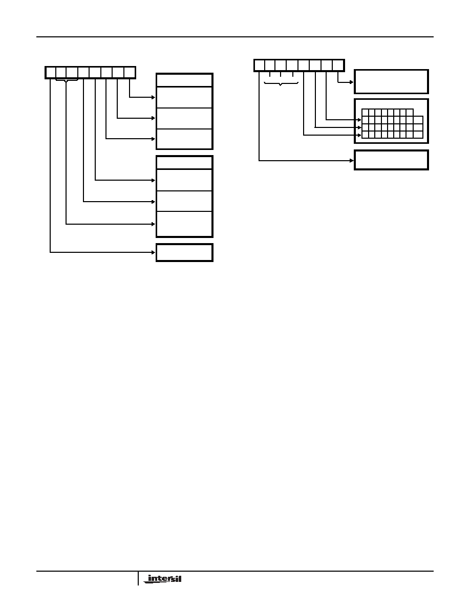
FIGURE 4. MODE DEFINITION FORMAT
D7 D6 D5 D4 D3 D2 D1 D0
PORT C (LOWER)
1 = INPUT
0 = OUTPUT
PORT B
1 = INPUT
0 = OUTPUT
MODE SELECTION
0 = MODE 0
1 = MODE 1
GROUP B
PORT C (UPPER)
1 = INPUT
0 = OUTPUT
PORT A
1 = INPUT
0 = OUTPUT
MODE SELECTION
00 = MODE 0
01 = MODE 1
GROUP A
1X = MODE 2
MODE SET FLAG
1 = ACTIVE
CONTROL WORD
FIGURE 5. BIT SET/RESET FORMAT
D7 D6 D5 D4 D3 D2 D1 D0
BIT SET/RESET
1 = SET
0 = RESET
BIT SELECT
0
BIT SET/RESET FLAG
CONTROL WORD
DON'T
CARE
X
X
X
0 = ACTIVE
1 2 3 4 5 6 7
0 1 0 1 0 1 0 1
0 0 1 1 0 0 1 1
0 0 0 0 1 1 1 1
B0
B1
B2
MS82C55A, MQ82C55A