 | –≠–ª–µ–∫—Ç—Ä–æ–Ω–Ω—ã–π –∫–æ–º–ø–æ–Ω–µ–Ω—Ç: DG303ABK | –°–∫–∞—á–∞—Ç—å:  PDF PDF  ZIP ZIP |
4-1
File Number
3119.2
CAUTION: These devices are sensitive to electrostatic discharge; follow proper IC Handling Procedures.
http://www.intersil.com or 407-727-9207 | Copyright © Intersil Corporation 1999
DG300A, DG301A, DG303A
TTL-Compatible, CMOS Analog Switches
The DG300A through DG303A family of monolithic CMOS
switches are truly compatible second source of the original
manufacturer. The switches are latch-proof and are
designed to block signals up to 30V
P-P
when OFF. Featuring
low leakage and low power consumption, these switches are
ideally suited for precision application in instrumentation,
communication, data acquisition and battery powered
applications. Other key features include Break-Before-Make
switching, TTL and CMOS compatibility, and low ON
resistance. Single supply operation (for positive switch
voltages) is possible by connecting V- to 0V.
Features
∑ Low Power Consumption
∑ Break-Before-Make Switching
- t
ON
. . . . . . . . . . . . . . . . . . . . . . . . . . . . . . . . . . . . 150ns
- t
OFF
. . . . . . . . . . . . . . . . . . . . . . . . . . . . . . . . . . . 130ns
∑ TTL, CMOS Compatible
∑ Low r
DS(ON)
(Max) . . . . . . . . . . . . . . . . . . . . . . . . . . . 50
∑ Single Supply Operation
∑ True Second Source
Ordering Information
PART NUMBER
TEMP.
RANGE (
o
C)
PACKAGE
PKG.
NO.
DG300ABK
-25 to 85
14 Ld CERDIP
F14.3
DG301ACJ
0 to 70
14 Ld PDIP
E14.3
DG303AAK
-55 to 125
14 Ld CERDIP
F14.3
DG303ABK
-25 to 85
14 Ld CERDIP
F14.3
DG303ACJ
0 to 70
14 Ld PDIP
E14.3
DG303ACY
0 to 70
16 Ld SOIC
M16.3
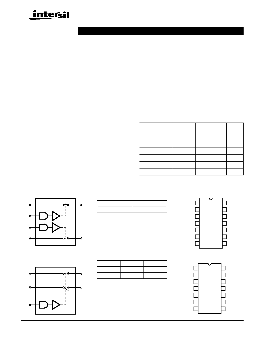
Functional Diagrams and Pinouts
(Switches shown for a logic "1" input)
DG300A
(SPST)
DG300A (CERDIP)
TOP VIEW
DG301A
(SPDT)
DG301A (PDIP)
TOP VIEW
S
1
IN
1
IN
2
S
2
D
1
D
2
DG300A TRUTH TABLE
LOGIC
SWITCH
0
OFF
1
ON
Logic "0"
0.8V, Logic "1"
4.0V.
NC
D
1
NC
S
1
NC
IN
1
GND
V+
D
2
NC
S
2
NC
IN
2
V-
1
2
3
4
5
6
7
14
13
12
11
10
9
8
S
1
S
2
IN
D
1
D
2
DG301A TRUTH TABLE
LOGIC
SWITCH 1
SWITCH 2
0
OFF
ON
1
ON
OFF
Logic "0"
0.8V, Logic "1"
4.0V.
NC
D
1
NC
S
1
NC
IN
GND
V+
D
2
NC
S
2
NC
NC
V-
1
2
3
4
5
6
7
14
13
12
11
10
9
8
Data Sheet
June 1999
4-2
Pin Descriptions
DG303A
(SPDT)
DG303A (CERDIP, PDIP)
TOP VIEW
DG303ACY (SOIC)
TOP VIEW
Functional Diagrams and Pinouts
(Switches shown for a logic "1" input) (Continued)
S
1
S
3
IN
1
D
1
D
3
S
4
S
2
IN
2
D
4
D
2
NC
S
3
D
3
D
1
S
1
IN
1
GND
V+
S
4
D4
D
2
S
2
IN
2
V-
1
2
3
4
5
6
7
14
13
12
11
10
9
8
14
15
16
9
13
12
11
10
1
2
3
4
5
7
6
8
NC
S
3
D
3
D
1
S
1
IN
1
NC
GND
V+
D
4
D
2
S
2
IN
2
V-
NC
S
4
DG303A TRUTH TABLE
LOGIC
SWITCH 1 AND 2
SWITCH 3 AND 4
0
OFF
ON
1
ON
OFF
Logic "0"
0.8V, Logic "1"
4.0V.
PIN
SYMBOL
DESCRIPTION
DG300A
1
NC
No Connection
2
D
1
Drain (Output) Terminal for Switch 1
3
NC
No Connection
4
S
1
Source (Input) Terminal for Switch 1
5
NC
No Connection
6
IN
1
Logic Control for Switch 1
7
GND
Ground Terminal (Logic Common)
8
V-
Negative Power Supply Terminal
9
IN
2
Logic Control for Switch 2
10
NC
No Connection
11
NC
No Connection
12
S
2
Source (Input) Terminal for Switch 2
13
D
2
Drain (Output) Terminal for Switch 2
14
V+
Positive Power Supply Terminal
DG301A
1
NC
No Connection
2
D
1
Drain (Output) Terminal for Switch 1
3
NC
No Connection
4
S
1
Source (Input) Terminal for Switch 1
5
IN
Logic Control for Switches
6
GND
Ground Terminal (Logic Common)
7
V-
Negative Power Supply Terminal
8
NC
No Connection
9
NC
No Connection
10
S
2
Source (Input) Terminal for Switch 2
11
NC
No Connection
12
D
2
Drain (Output) Terminal for Switch 2
13
NC
No Connection
14
V+
Positive Power Supply Terminal
DG303A
1
NC
No Connection
2
S
3
Source (Input) Terminal for Switch 3
3
D
3
Drain (Output) Terminal for Switch 3
4
D
1
Drain (Output) Terminal for Switch 1
5
S
1
Source (Input) Terminal for Switch 1
6
IN
1
Logic Control for Switch 1
7
GND
Ground Terminal (Logic Common)
8
V-
Negative Power Supply Terminal
9
IN
2
Logic Control for Switch 2
10
S
2
Source (Input) Terminal for Switch 2
11
D
2
Drain (Output) Terminal for Switch 2
12
D
4
Drain (Output) Terminal for Switch 4
13
S
4
Source (Input) Terminal for Switch 4
14
V+
Positive Power Supply Terminal
PIN
SYMBOL
DESCRIPTION
DG300A, DG301A, DG303A
4-3
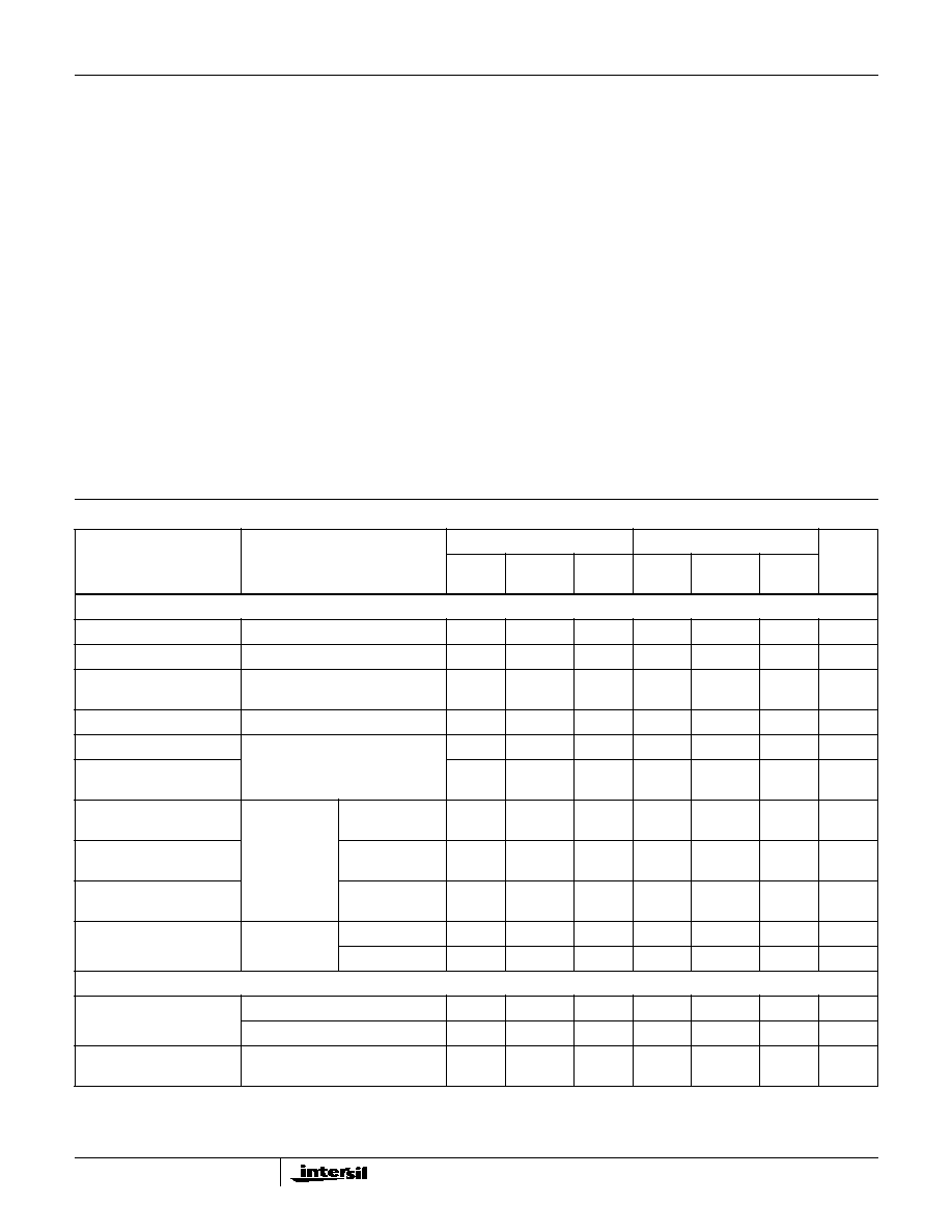
Absolute Maximum Ratings
Thermal Information
V+ to V- . . . . . . . . . . . . . . . . . . . . . . . . . . . . . . . . . . . . . . . . . . 44.0V
V- to GND. . . . . . . . . . . . . . . . . . . . . . . . . . . . . . . . . . . . . . . . . . 25V
Digital Inputs, V
S
, V
D
(Note 1) . . . . . . . . . . . . . (V-) - 2V to (V+) + 2V
or 30mA, Whichever Occurs First
Continuous Current, (Any Terminal). . . . . . . . . . . . . . . . . . . . . 30mA
Peak Current, S or D (Pulsed 1ms, 10% Duty Cycle Max) . . 100mA
Operating Conditions
Voltage Range . . . . . . . . . . . . . . . . . . . . . . . . . . . . . . . . . . . . .
±
15V
Temperature Range
"A" Suffix. . . . . . . . . . . . . . . . . . . . . . . . . . . . . . . . -55
o
C to 125
o
C
"B" Suffix. . . . . . . . . . . . . . . . . . . . . . . . . . . . . . . . . -25
o
C to 85
o
C
"C" Suffix . . . . . . . . . . . . . . . . . . . . . . . . . . . . . . . . . 0
o
C to 70
o
C
Input Low Voltage . . . . . . . . . . . . . . . . . . . . . . . . . . . . . 0.8V (Max)
Input High Voltage . . . . . . . . . . . . . . . . . . . . . . . . . . . . . . 4.0V (Min)
Input Rise and Fall Time . . . . . . . . . . . . . . . . . . . . . . . . . . . .
20ns
Thermal Resistance (Typical, Note 2)
JA
(
o
C/W)
JC
(
o
C/W)
SOIC Package . . . . . . . . . . . . . . . . . . .
100
N/A
PDIP Package . . . . . . . . . . . . . . . . . . .
100
N/A
CERDIP Package . . . . . . . . . . . . . . . . .
75
20
Maximum Junction Temperature
Hermetic Packages . . . . . . . . . . . . . . . . . . . . . . . . . . . . . . 175
o
C
Plastic Packages . . . . . . . . . . . . . . . . . . . . . . . . . . . . . . . . 150
o
C
Maximum Storage Temperature Range . . . . . . . . . . -65
o
C to 150
o
C
Maximum Lead Temperature (Soldering, 10s). . . . . . . . . . . . 300
o
C
(SOIC - Lead Tips Only)
CAUTION: Stresses above those listed in "Absolute Maximum Ratings" may cause permanent damage to the device. This is a stress only rating and operation of the
device at these or any other conditions above those indicated in the operational sections of this specification is not implied.
NOTES:
1. Signals on S
X
, D
X
or IN
X
exceeding V+ or V- will be clamped by internal diodes. Limit diode forward current to maximum current ratings.
2.
JA
is measured with the component mounted on an evaluation PC board in free air.
Electrical Specifications
V+ = +15V, V- = -15V, GND = 0V, T
A
= 25
o
C
PARAMETER
TEST CONDITIONS
"A" SUFFIX
"B" AND "C" SUFFIX
UNITS
MIN
(NOTE 3)
TYP
MAX
MIN
(NOTE 3)
TYP
MAX
DYNAMIC CHARACTERISTICS
Turn-ON Time, t
ON
See Figure 3
-
150
300
-
150
-
ns
Turn-OFF Time, t
OFF
See Figure 3
-
130
250
-
130
-
ns
Break-Before-Make
Interval, t
D
See Figure 2, DG301A/DG303A
-
50
-
-
50
-
ns
Charge Injection, Q
C
L
= 10nF, R
S
= 0, V
S
= 0
-
3
-
-
3
-
mV
OFF Isolation (Note 4)
V
IN
= 0, R
L
= 1k
, V
S
= 1V
RMS
,
f = 500kHz
-
62
-
-
62
-
dB
Crosstalk
(Channel-to-Channel)
-
-74
-
-
-74
-
dB
Source OFF Capacitance,
C
S(OFF)
f = 1MHz,
V
IN
= 0.8V or
V
IN
= 4.0V
V
S
= 0
-
14
-
-
14
-
pF
Drain OFF Capacitance,
C
D(OFF)
V
D
= 0
-
14
-
-
14
-
pF
Channel ON Capacitance,
C
D(ON)
+ C
S(ON)
V
S
= V
D
= 0
-
40
-
-
40
-
pF
Input Capacitance, C
IN
f = 1MHz
V
IN
= 0
-
6
-
-
6
-
pF
V
IN
= 15V
-
7
-
-
7
-
pF
DIGITAL INPUT CHARACTERISTICS
Input Current with Voltage
High, I
IH
V
IN
= 5.0V
-1
-0.001
-
-1
-0.001
-
µ
A
V
IN
= 15.0V
-
0.001
1
-
0.001
1
µ
A
Input Current with Voltage
Low, I
IL
V
IN
= 0V
-1
-0.001
-
-1
-0.001
-
µ
A
DG300A, DG301A, DG303A
4-4
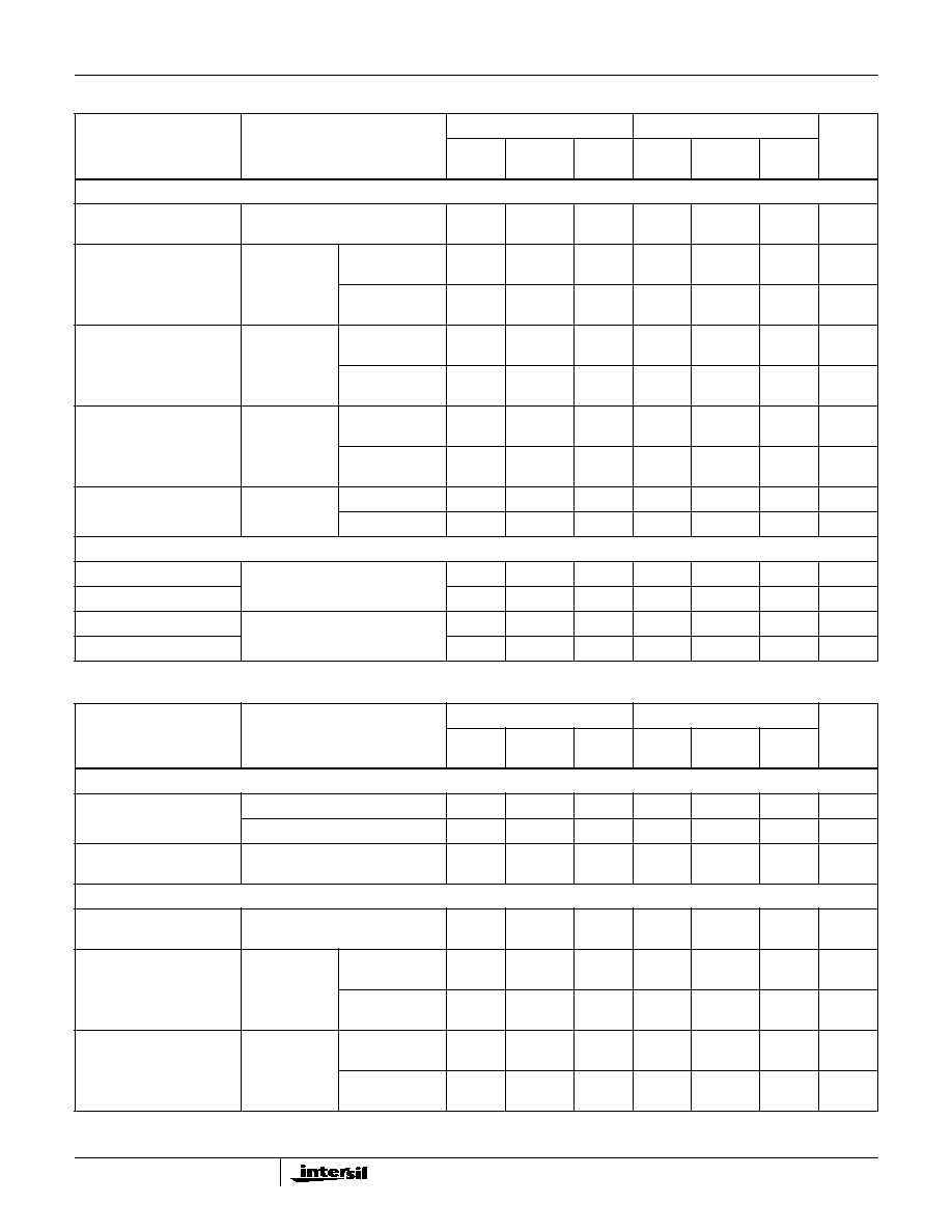
ANALOG SWITCH CHARACTERISTICS
Analog Signal Range,
V
ANALOG
I
S
= 10mA, V
IN
= 0.8V or 4V
-15
-
15
-15
-
15
V
Drain-Source ON
Resistance, r
DS(ON)
V
IN
= 0.8V or
V
IN
= 4.0V
I
S
= -10mA,
V
D
= 10V
-
30
50
-
30
50
I
S
= 10mA,
V
D
= -10V
-
30
50
-
30
50
Source OFF Leakage
Current, I
S(OFF)
V
IN
= 0.8V or
V
IN
= 4.0V
V
S
= 14V,
V
D
= -14V
-
0.1
1
-
0.1
5
nA
V
S
= -14V,
V
D
= 14V
-1
-0.1
-
-5
-0.1
-
nA
Drain OFF Leakage
Current, I
D(OFF)
V
IN
= 0.8V or
V
IN
= 4.0V
V
S
= -14V,
V
D
= 14V
-
0.1
1
-
0.1
5
nA
V
S
= 14V,
V
D
= -14V
-1
-0.1
-
-5
-0.1
-
nA
Channel ON Leakage
Current, I
D(ON)
V
IN
= 0.8V or
V
IN
= 4.0V
V
D
= V
S
= 14V
-
0.1
1
-
0.1
5
nA
V
D
= V
S
= -14V
-2
-0.1
-
-5
-0.1
-
nA
POWER SUPPLY CHARACTERISTICS
Positive Supply Current, I+
V
IN
= 4V (One Input)
(All Others = 0)
-
0.23
0.5
-
0.23
0.5
mA
Negative Supply Current, I-
-10
-0.001
-
-10
-0.001
-
µ
A
Positive Supply Current, I+
V
IN
= 0.8V (All Inputs)
-
0.001
10
-
0.001
10
µ
A
Negative Supply Current, I-
-10
-0.001
-
-10
-0.001
-
µ
A
Electrical Specifications
V+ = +15V, V- = -15V, GND = 0V, T
A
= 25
o
C (Continued)
PARAMETER
TEST CONDITIONS
"A" SUFFIX
"B" AND "C" SUFFIX
UNITS
MIN
(NOTE 3)
TYP
MAX
MIN
(NOTE 3)
TYP
MAX
Electrical Specifications
V+ = +15V, V- = -15V, GND = 0V, T
A
= Full Temperature Range
PARAMETER
TEST CONDITION
"A" SUFFIX
"B" AND "C" SUFFIX
UNITS
MIN
(NOTE 3)
TYP
MAX
MIN
(NOTE 3)
TYP
MAX
DIGITAL INPUT CHARACTERISTICS
Input Current with Voltage
High, I
IH
V
IN
= 5.0V
-1
-
-
-
-
-
µ
A
V
IN
= 15.0V
-
-
1
-
-
-
µ
A
Input Current with Voltage
Low, I
IL
V
IN
= 0V
-1
-
-
-
-
-
µ
A
ANALOG SWITCH CHARACTERISTICS
Analog Signal Range,
V
ANALOG
I
S
= 10mA, V
IN
= 0.8V or 4V
-15
-
15
-
-
-
V
Drain-Source ON
Resistance, r
DS(ON)
V
IN
= 0.8V or
V
IN
= 4.0V
I
S
= -10mA,
V
D
= 10V
-
-
75
-
-
-
I
S
= 10mA,
V
D
= -10V
-
-
75
-
-
-
Source OFF Leakage
Current, I
S(OFF)
V
IN
= 0.8V or
V
IN
= 4.0V
V
S
= 14V,
V
D
= -14V
-
-
100
-
-
-
nA
V
S
= -14V,
V
D
= 14V
-100
-
-
-
-
-
nA
DG300A, DG301A, DG303A
4-5
Drain OFF Leakage
Current, I
D(OFF)
V
IN
= 0.8V or
V
IN
= 4.0V
V
S
= -14V,
V
D
= 14V
-
-
100
-
-
-
nA
V
S
= 14V,
V
D
= -14V
-100
-
-
-
-
nA
Channel ON Leakage
Current, I
D(ON)
V
IN
= 0.8V or
V
IN
= 4.0V
V
D
= V
S
= 14V
-
-
100
-
-
-
nA
V
D
= V
S
= -14V
-200
-
-
-
-
-
nA
POWER SUPPLY CHARACTERISTICS
Positive Supply Current, I+
V
IN
= 4V (One Input)
(All Others = 0)
-
-
1
-
-
-
mA
Negative Supply Current, I-
-100
-
-
-
-
-
µ
A
Positive Supply Current, I+
V
IN
= 0.8V (All Inputs)
-
-
100
-
-
-
µ
A
Negative Supply Current, I-
-100
-
-
-
-
-
µ
A
NOTES:
3. For design only, not 100% tested.
4. OFF isolation = 20 Log V
S
/V
D
, where V
S
= input to OFF switch, and V
D
= output.
Electrical Specifications
V+ = +15V, V- = -15V, GND = 0V, T
A
= Full Temperature Range (Continued)
PARAMETER
TEST CONDITION
"A" SUFFIX
"B" AND "C" SUFFIX
UNITS
MIN
(NOTE 3)
TYP
MAX
MIN
(NOTE 3)
TYP
MAX
Test Circuits and Waveforms
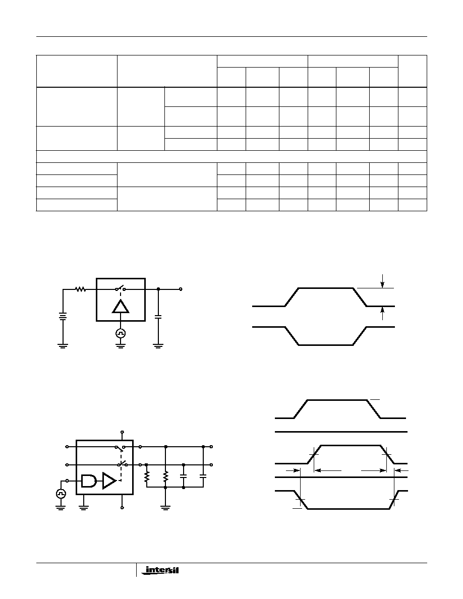
FIGURE 1. CHARGE INJECTION TEST CIRCUIT AND MEASUREMENT POINTS
FIGURE 2. BREAK-BEFORE MAKE TEST CIRCUIT AND MEASUREMENT POINTS (DG301A, DG303A)
R
S
S
X
C
L
= 10nF
V
D
D
X
IN
X
V
S
V
D
IN
X
V
O
ON
OFF
ON
V
O1
LOGIC "1" = SWITCH ON
V
O2
S
1
S
2
IN
V
S1
= 3V
LOGIC
INPUT
GND
V
S2
= 3V
R
L2
300
R
L1
300
C
L2
33pF
C
L1
33pF
SWITCH
OUTPUT
15V
V+
-15V
V-
50%
t
D
50%
0V
LOGIC
INPUT
SWITCH
OUTPUT
SWITCH
OUTPUT
V
S1
0V
V
S2
0V
D
1
D
2
(V
O1
)
(V
O2
)
0V
5V
DG300A, DG301A, DG303A