1
File Number
3120.3
DG308A
Quad Monolithic SPST, CMOS Analog
Switch
The DG308A quad monolithic SPST, CMOS switch is latch
proof and is designed to block signals up to 30V
P-P
when
OFF. Featuring low ON resistance, low power consumption,
and rail-to-rail analog signal range, this switch is ideally
suited for high speed switching applications in
communications, instrumentation and process control. The
DG308A has single and dual supply capability. The input
thresholds are CMOS compatible.
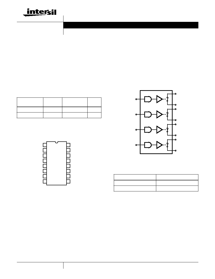
Pinout
DG308A
(PDIP, SOIC)
TOP VIEW
Features
∑ Low Power Consumption
∑ CMOS Compatible
∑
±
15V Analog Signal Range
∑ Single or Dual Supply Capability
∑ Alternate Source
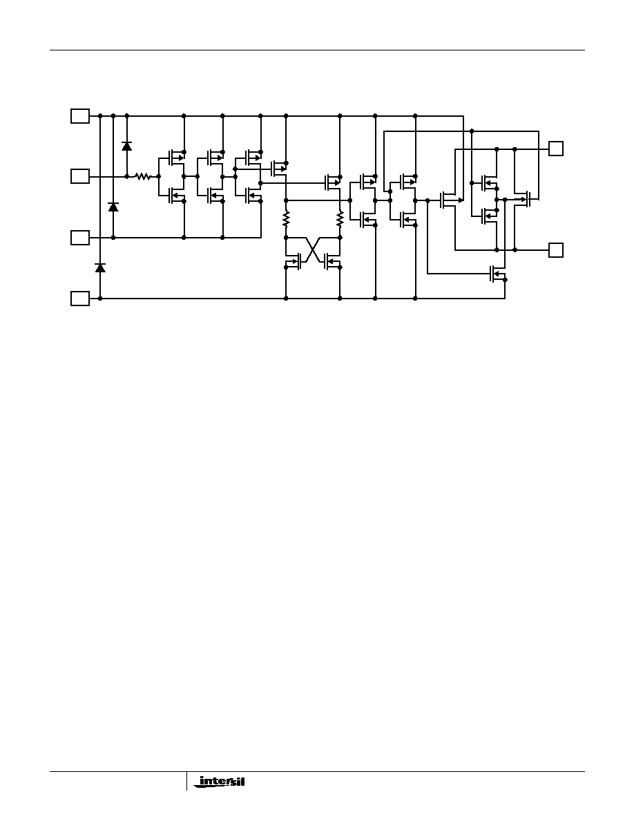
Functional Diagram
Ordering Information
PART NUMBER
TEMP.
RANGE (
o
C)
PACKAGE
PKG.
NO.
DG308ACJ
0 to 70
16 Ld PDIP
E16.3
DG308ACY
0 to 70
16 Ld SOIC
M16.15
IN
1
D
1
S
1
V-
GND
S
4
IN
4
D
4
IN
2
S
2
V+ (SUB-
NC
S
3
D
3
IN
3
D
2
STRATE)
-
14
15
16
9
13
12
11
10
1
2
3
4
5
7
6
8
TRUTH TABLE
LOGIC
DG308A
0
OFF
1
ON
Logic "0"
3.5V, Logic "1"
11V at V+ = 15V.
IN
1
S
1
D
1
IN
2
S
2
D
2
IN
3
S
3
D
3
IN
4
S
4
D
4
DG308A
SWITCHES SHOWN FOR LOGIC "1" INPUT
Data Sheet
November 1999
CAUTION: These devices are sensitive to electrostatic discharge; follow proper IC Handling Procedures.
1-888-INTERSIL or 321-724-7143
|
Copyright
©
Intersil Corporation 1999
3
Absolute Maximum Ratings
Thermal Information
V+ to V- . . . . . . . . . . . . . . . . . . . . . . . . . . . . . . . . . . . . . . . . . . . 44V
V- to Ground. . . . . . . . . . . . . . . . . . . . . . . . . . . . . . . . . . . . . . . . 25V
Digital Inputs, V
S
, V
D
(Note 1) . . . . . . . . . . . . . . (V-) -2V to (V+) +2V
or 30mA, Whichever Comes First
Continuous Current, (Any Terminal Except S) . . . . . . . . . . . . . 30mA
Continuous Current, (S or D) . . . . . . . . . . . . . . . . . . . . . . . . . . 20mA
Peak Current, S or D (Pulsed 1ms, 10% Duty Cycle Max) . . . . . 70mA
Operating Conditions
Temperature Range
"C" Suffix . . . . . . . . . . . . . . . . . . . . . . . . . . . . . . . . . 0
o
C to 70
o
C
Thermal Resistance (Typical, Note 2)
JA
(
o
C/W)
PDIP Package . . . . . . . . . . . . . . . . . . . . . . . . . . . . .
90
SOIC Package . . . . . . . . . . . . . . . . . . . . . . . . . . . . .
115
Maximum Junction Temperature . . . . . . . . . . . . . . . . . . . . . . .150
o
C
Maximum Storage Temperature Range . . . . . . . . . . . 65
o
C to 150
o
C
Maximum Lead Temperature (Soldering 10s) . . . . . . . . . . . . 300
o
C
(SOIC - Lead Tips Only)
CAUTION: Stresses above those listed in "Absolute Maximum Ratings" may cause permanent damage to the device. This is a stress only rating and operation of the
device at these or any other conditions above those indicated in the operational sections of this specification is not implied.
NOTES:
1. Signals on S
X
, D
X
, or IN
X
exceeding V+ or V- will be clamped by internal diodes. Limit forward diode current to maximum current ratings.
2.
JA
is measured with the component mounted on an evaluation PC board in free air.
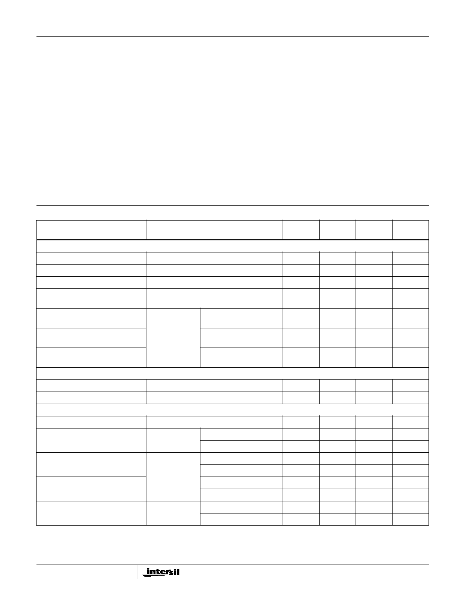
Electrical Specifications
V+ = 15V, V- = -15V, GND = 0V, T
A
= 25
o
C
PARAMETER
TEST CONDITIONS
(NOTE 4)
MIN
(NOTE 3)
TYP
(NOTE 4)
MAX
UNITS
DYNAMIC CHARACTERISTICS
Turn-ON Time, t
ON
See Figure 1
-
130
200
ns
Turn-OFF Time, t
OFF
See Figure 1
-
90
150
ns
Charge Injection, Q
C
L
= 1
µ
F, R
S
= 0, V
S
= 0V
-
-10
-
pC
OFF Isolation, OIRR
V
IN
= 0V, R
L
= 75
, V
S
= 2V
P-P
, f = 500kHz
(Note 5)
-
78
-
dB
Source OFF Capacitance, C
S(OFF)
f = 140kHz
V
S
= 0V
V
IN
= 0V
-
11
-
pF
Drain OFF Capacitance, C
D(OFF)
V
D
= 0V
V
IN
= 0V
-
8
-
pF
Channel ON Capacitance,
C
D(ON)
+ C
S(ON)
V
S
= V
D
= 0V
V
IN
= 15V
-
27
-
pF
DIGITAL INPUT CHARACTERISTICS
Input Current with Voltage High, I
IH
V
IN
= 15V, Full Temperature Range
-
0.001
1
µ
A
Input Current with Voltage Low, I
IL
V
IN
= 0V, Full Temperature Range
-1
-0.001
-
µ
A
ANALOG SWITCH CHARACTERISTICS
Analog Signal Range, V
ANALOG
-15
-
15
V
Drain-Source ON Resistance, r
DS(ON)
V
IN
= 11V
I
S
= -1mA, V
D
= +10V
-
60
100
I
S
= 1mA, V
D
= -10V
-
60
100
Source OFF Leakage Current, I
S(OFF)
V
IN
= 3.5V
V
S
= 14V, V
D
= -14V
-
0.1
5
nA
V
S
= -14V, V
D
= 14V
-5
-0.1
-
nA
Drain OFF Leakage Current, I
D(OFF)
V
S
= -14V, V
D
= 14V
-
0.1
5
nA
V
S
= 14V, V
D
= -14V
-5
-0.1
-
nA
Channel ON Leakage Current, I
D(ON)
V
IN
= 11V
V
D
= V
S
= 14V
-
0.1
5
nA
V
D
= V
S
= -14V
-5
-0.1
-
nA
DG308A

4
Test Circuit and Waveforms
POWER SUPPLY CHARACTERISTICS
Positive Supply Current, I+
All Channels ON or OFF
V
IN
= 0V or 15V
-
0.001
100
µ
A
Negative Supply Current, I-
-100
-0.001
-
µ
A
NOTES:
3. Typical values are for design aid only, not guaranteed and not subject to production testing.
4. The algebraic convention whereby the most negative value is a minimum, and the most positive is a maximum, is used in this data sheet.
5. OFF isolation = 20 Log V
D
/V
S
, where V
S
= input to OFF switch, and V
D
= output.
Electrical Specifications
V+ = 15V, V- = -15V, GND = 0V, T
A
= 25
o
C (Continued)
PARAMETER
TEST CONDITIONS
(NOTE 4)
MIN
(NOTE 3)
TYP
(NOTE 4)
MAX
UNITS
V
O
S
IN
GND
V
S
= 3V
R
L
1k
C
L
35pF
15V
V+
-15V
V-
V
O
= V
S
R
L
R
L
+ r
DS(ON)
50%
t
r
< 20ns
t
f
< 20ns
t
OFF
t
ON
LOGIC
INPUT
SWITCH
INPUT
SWITCH
OUTPUT
90%
D
50%
90%
LOGIC "1" = SWITCH ON
FIGURE 1. t
ON
AND t
OFF
TEST CIRCUIT AND MEASUREMENT POINTS
15V
0V
0V
DG308A