 | –≠–ª–µ–∫—Ç—Ä–æ–Ω–Ω—ã–π –∫–æ–º–ø–æ–Ω–µ–Ω—Ç: DG408DJ | –°–∫–∞—á–∞—Ç—å:  PDF PDF  ZIP ZIP |
1
File Number
3283.5
DG408, DG409
Single 8-Channel/Differential 4-Channel,
CMOS Analog Multiplexers
The DG408 Single 8-Channel, and DG409 Differential
4-Channel monolithic CMOS analog multiplexers are drop-in
replacements for the popular DG508A and DG509A series
devices. They each include an array of eight analog
switches, a TTL/CMOS compatible digital decode circuit for
channel selection, a voltage reference for logic thresholds
and an ENABLE input for device selection when several
multiplexers are present.
The DG408 and DG409 feature lower signal ON resistance
(<100
) and faster switch transition time (t
TRANS
< 250ns)
compared to the DG508A or DG509A. Charge injection has
been reduced, simplifying sample and hold applications. The
improvements in the DG408 series are made possible by
using a high-voltage silicon-gate process. An epitaxial layer
prevents the latch-up associated with older CMOS
technologies. Power supplies may be single-ended from +5V
to +34V, or split from
±
5V to
±
20V.
The analog switches are bilateral, equally matched for AC or
bidirectional signals. The ON resistance variation with
analog signals is quite low over a
±
5V analog input range.
Features
∑ ON Resistance (Max, 25
o
C). . . . . . . . . . . . . . . . . . . 100
∑ Low Power Consumption (P
D
) . . . . . . . . . . . . . . . <11mW
∑ Fast Switching Action
- t
TRANS
. . . . . . . . . . . . . . . . . . . . . . . . . . . . . . . . <250ns
- t
ON/OFF(EN)
. . . . . . . . . . . . . . . . . . . . . . . . . . . . <150ns
∑ Low Charge Injection
∑ Upgrade from DG508A/DG509A
∑ TTL, CMOS Compatible
∑ Single or Split Supply Operation
Applications
∑ Data Acquisition Systems
∑ Audio Switching Systems
∑ Automatic Testers
∑ Hi-Rel Systems
∑ Sample and Hold Circuits
∑ Communication Systems
∑ Analog Selector Switch
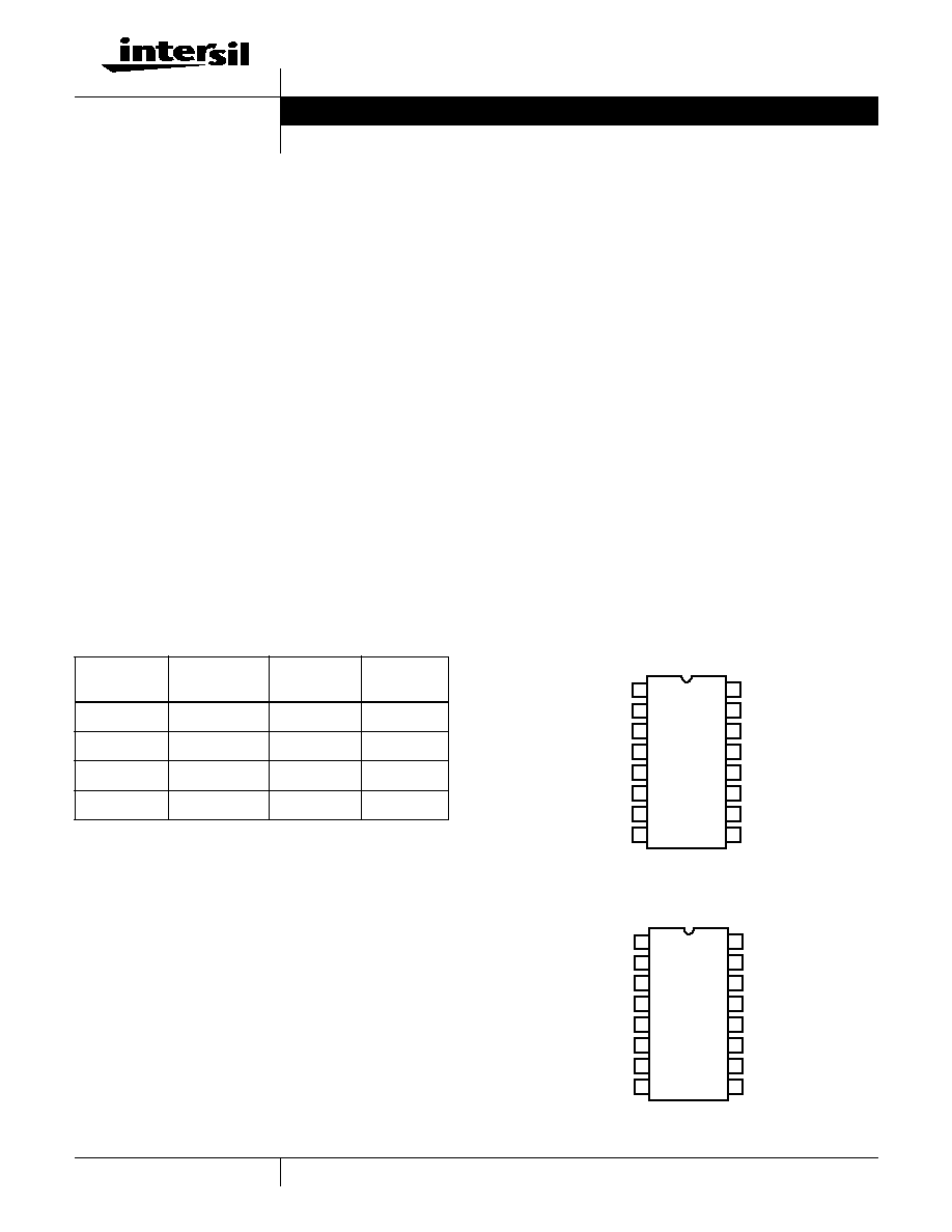
Pinouts
DG408 (PDIP, SOIC)
TOP VIEW
DG409 (PDIP, SOIC)
TOP VIEW
Ordering Information
PART
NUMBER
TEMP. RANGE
(
o
C)
PACKAGE
PKG. NO.
DG408DJ
-40 to 85
16 Ld PDIP
E16.3
DG408DY
-40 to 85
16 Ld SOIC
M16.15
DG409DJ
-40 to 85
16 Ld PDIP
E16.3
DG409DY
-40 to 85
16 Ld SOIC
M16.15
14
15
16
9
13
12
11
10
1
2
3
4
5
7
6
8
A
0
EN
V-
S
1
S
2
S
3
D
S
4
A
1
GND
V+
S
5
S
6
S
7
S
8
A
2
14
15
16
9
13
12
11
10
1
2
3
4
5
7
6
8
A
0
EN
V-
S
1A
S
2A
S
3A
D
A
S
4A
A
1
V+
S
1B
S
3B
S
4B
D
B
GND
S
2B
Data Sheet
June 1999
CAUTION: These devices are sensitive to electrostatic discharge; follow proper IC Handling Procedures.
http://www.intersil.com or 407-727-9207
|
Copyright
©
Intersil Corporation 1999
2
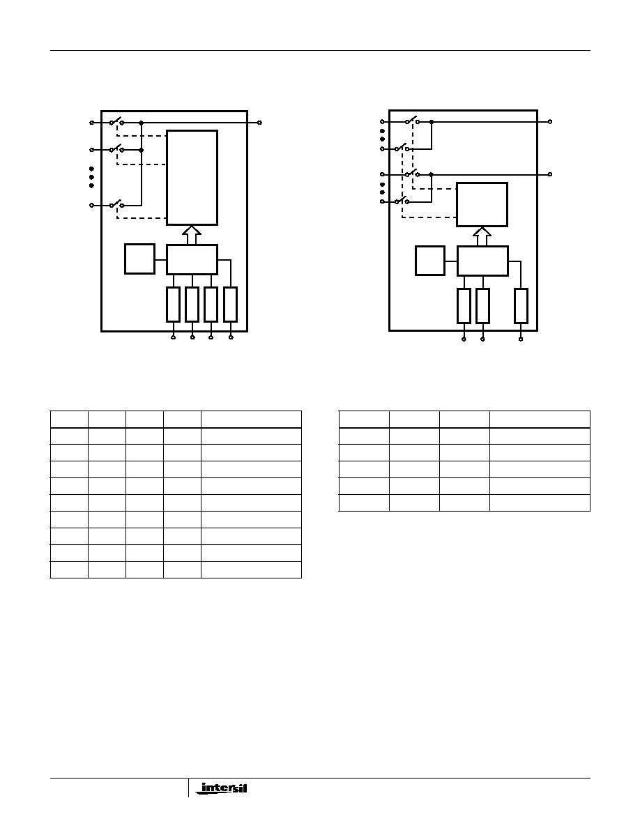
Functional Block Diagrams
DG408
DG409
TRUTH TABLE DG408
A
2
A
1
A
0
EN
ON SWITCH
X
X
X
0
NONE
0
0
0
1
1
0
0
1
1
2
0
1
0
1
3
0
1
1
1
4
1
0
0
1
5
1
0
1
1
6
1
1
0
1
7
1
1
1
1
8
DECODER/
DRIVER
D
LEVEL
SHIFT
5V
REF
DIGITAL
INPUT
PROTECTION
S
1
S
2
S
8
A
0
A
1
A
2
EN
TRUTH TABLE DG409
A
1
A
0
EN
ON SWITCH
X
X
0
NONE
0
0
1
1
0
1
1
2
1
0
1
3
1
1
1
4
NOTES:
1. V
AH
Logic "1"
2.4V.
2. V
AL
Logic "0"
0.8V.
DECODER/
DRIVER
D
A
LEVEL
SHIFT
5V
REF
DIGITAL
INPUT
PROTECTION
S
1A
S
4A
S
1B
A
0
A
1
EN
D
B
S
4B
DG408, DG409
3
Pin Descriptions - (DG408)
PIN
SYMBOL
DESCRIPTION
1
A
0
Logic Decode Input (Bit 0, LSB)
2
EN
Enable Input
3
V-
Negative Power Supply Terminal
4
S
1
Source (Input) for Channel 1
5
S
2
Source (Input) for Channel 2
6
S
3
Source (Input) for Channel 3
7
S
4
Source (Input) for Channel 4
8
D
Drain (Output)
9
S
8
Source (Input) for Channel 8
10
S
7
Source (Input) for Channel 7
11
S
6
Source (Input) for Channel 6
12
S
5
Source (Input) for Channel 5
13
V+
Positive Power Supply Terminal (Substrate)
14
GND
Ground Terminal (Logic Common)
15
A
2
Logic Decode Input (Bit 2, MSB)
16
A
1
Logic Decode Input (Bit 1)
Pin Descriptions - (DG409)
PIN
SYMBOL
DESCRIPTION
1
A
0
Logic Decode Input (Bit 0, LSB)
2
EN
Enable Input
3
V-
Negative Power Supply Terminal
4
S
1A
Source (Input) for Channel 1a
5
S
2A
Source (Input) for Channel 2a
6
S
3A
Source (Input) for Channel 3a
7
S
4A
Source (Input) for Channel 4a
8
D
A
Drain a (Output a)
9
D
B
Drain b (Output b)
10
S
4B
Source (Input) for Channel 4b
11
S
3B
Source (Input) for Channel 3b
12
S
2B
Source (Input) for Channel 2b
13
S
1B
Source (Input) for Channel 1b
14
V+
Positive Power Supply Terminal
15
GND
Ground Terminal (Logic Common)
16
A
1
Logic Decode Input (Bit 1, MSB)
DG408, DG409
4
Absolute Maximum Ratings
Thermal Information
V+ to V- . . . . . . . . . . . . . . . . . . . . . . . . . . . . . . . . . . . . . . . . . . 44.0V
GND to V-. . . . . . . . . . . . . . . . . . . . . . . . . . . . . . . . . . . . . . . . . . .25V
Digital Inputs, V
S
, V
D
(Note 3). . . . . .(V-) -2V to (V+) + 2V or 20mA,
Whichever Occurs First
Continuous Current (Any Terminal) . . . . . . . . . . . . . . . . . . . . . 30mA
Peak Current, S or D (Pulsed 1ms, 10% Duty Cycle Max) . . 100mA
Operating Conditions
Temperature Range . . . . . . . . . . . . . . . . . . . . . . . . . . -40
o
C to 85
o
C
Thermal Resistance (Typical, Note 4)
JA
(
o
C/W)
PDIP Package . . . . . . . . . . . . . . . . . . . . . . . . . . . . .
90
SOIC Package . . . . . . . . . . . . . . . . . . . . . . . . . . . . .
110
Maximum Junction Temperature . . . . . . . . . . . . . . . . . . . . . . .150
o
C
Maximum Storage Temperature Range . . . . . . . . . . -65
o
C to 125
o
C
Maximum Lead Temperature (Soldering 10s) . . . . . . . . . . . . .300
o
C
(SOIC - Lead Tips Only)
CAUTION: Stresses above those listed in "Absolute Maximum Ratings" may cause permanent damage to the device. This is a stress only rating and operation of the
device at these or any other conditions above those indicated in the operational sections of this specification is not implied.
NOTES:
3. Signals on S
X
, D
X
, EN or A
X
exceeding V+ or V- are clamped by internal diodes. Limit diode current to maximum current ratings.
4.
JA
is measured with the component mounted on an evaluation PC board in free air.
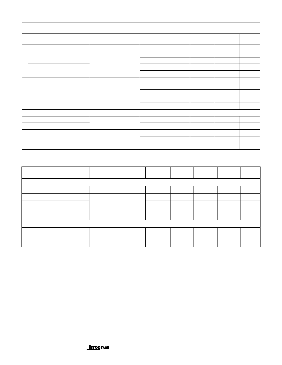
Electrical Specifications
Test Conditions: V+ = +15V, V- = -15V, V
AL
= 0.8V, V
AH
= 2.4V, Unless Otherwise Specified
PARAMETER
TEST CONDITIONS
TEMP (
o
C)
(NOTE 5)
MIN
(NOTE 6)
TYP
(NOTE 5)
MAX
UNITS
DYNAMIC CHARACTERISTICS
Transition Time, t
TRANS
(See Figure 1)
Full
-
160
250
ns
Break-Before-Make Interval, t
OPEN
(See Figure 3)
25
10
-
-
ns
Enable Turn-ON Time, t
ON(EN)
(See Figure 2)
25
-
115
150
ns
Full
-
-
225
ns
Enable Turn-OFF Time, t
OFF(EN)
(See Figure 2)
Full
-
105
150
ns
Charge Injection, Q
C
L
= 10nF, V
S
= 0V
25
-
20
-
pC
OFF Isolation
V
EN
= 0V, R
L
= 1k
,
f = 100kHz (Note 9)
25
-
-75
-
dB
Logic Input Capacitance, C
IN
f = 1MHz
25
-
8
-
pF
Source OFF Capacitance, C
S(OFF)
V
EN
= 0V, V
S
= 0V,
f = 1MHz
25
-
3
-
pF
Drain OFF Capacitance, C
D(OFF)
V
EN
= 0V, V
D
= 0V,
f = 1MHz
DG408
25
-
26
-
pF
DG409
25
-
14
-
pF
Drain ON Capacitance, C
D(ON)
V
EN
= 3V, V
D
= 0V,
f = 1MHz, V
A
= 0V or 3V
DG408
25
-
37
-
pF
DG409
25
-
25
-
pF
DIGITAL INPUT CHARACTERISTICS
Logic Input Current,
Input Voltage High, I
AH
V
A
= 2.4V, 15V
Full
-10
-
10
µ
A
Logic Input Current,
Input Voltage Low, I
AL
V
EN
= 0V, 2.4V,
V
A
= 0V
Full
-10
-
10
µ
A
ANALOG SWITCH CHARACTERISTICS
Analog Signal Range, V
ANALOG
Full
-15
-
15
V
Drain-Source ON Resistance,
r
DS(ON)
V
D
=
±
10V, I
S
= -10mA
(Note 7)
25
-
40
100
Full
-
-
125
r
DS(ON)
Matching Between Channels,
r
DS(ON)
V
D
= 10V, -10V (Note 8)
25
-
-
15
Source OFF Leakage Current, I
S(OFF)
V
EN
= 0V, V
S
=
±
10V,
V
D
= +10V
25
-0.5
-
0.5
nA
Full
-5
-
5
nA
DG408, DG409
5
Drain OFF Leakage Current, I
D(OFF)
V
EN
= 0V, V
D
=
±
10V,
V
S
= +10V
DG408
25
-1
-
1
nA
Full
-20
-
20
nA
DG409
25
-1
-
1
nA
Full
-10
-
10
nA
Drain ON Leakage Current, I
D(ON)
V
S
= V
D
=
±
10V (Note 7)
DG408
25
-1
-
1
nA
Full
-20
-
20
nA
DG409
25
-1
-
1
nA
Full
-10
-
10
nA
POWER SUPPLY CHARACTERISTICS
Positive Supply Current, I+
V
EN
= 0V, V
A
= 0V (Standby)
Full
-
10
75
µ
A
Negative Supply Current, I-
Full
-75
1
-
µ
A
Positive Supply Current, I+
V
EN
= 2.4V, V
A
= 0V
(Enabled)
25
-
0.2
0.5
mA
Full
-
-
2
mA
Negative Supply Current, I-
Full
-500
-
-
µ
A
Electrical Specifications
Test Conditions: V+ = +15V, V- = -15V, V
AL
= 0.8V, V
AH
= 2.4V, Unless Otherwise Specified (Continued)
PARAMETER
TEST CONDITIONS
TEMP (
o
C)
(NOTE 5)
MIN
(NOTE 6)
TYP
(NOTE 5)
MAX
UNITS
Electrical Specifications
Single Supply Test Conditions: V+ = 12V, V- = 0V, V
AL
= 0.8V, V
AH
= 2.4V,
Unless Otherwise Specified
PARAMETER
TEST
CONDITION
TEMP (
o
C)
(NOTE 5)
MIN
(NOTE 6)
TYP
(NOTE 5)
MAX
UNITS
DYNAMIC CHARACTERISTICS
Switching Time of Multiplexer, t
TRANS
V
S1
= 8V, V
S8
= 0V, V
IN
= 2.4V
25
-
180
-
ns
Enable Turn-ON Time, t
ON(EN)
V
INH
= 2.4V, V
INL
= 0V,
V
S1
= 5V
25
-
180
-
ns
Enable Turn-OFF Time, t
OFF(EN)
25
-
120
-
ns
Charge Injection, Q
C
L
= 10nF, V
GEN
= 0V,
R
GEN
= 0
25
-
5
-
pC
ANALOG SWITCH CHARACTERISTICS
Analog Signal Range, V
ANALOG
Full
0
-
12
V
Drain-Source ON-Resistance,
r
DS(ON)
V
D
= 3V, 10V, I
S
= -1mA
(Note 7)
25
-
90
-
NOTES:
5. The algebraic convention whereby the most negative value is a minimum and the most positive a maximum, is used in this data sheet.
6. Typical values are for DESIGN AID ONLY, not guaranteed nor production tested.
7. Sequence each switch ON.
8.
r
DS(ON)
= r
DS(ON)
(Max) - r
DS(ON)
(Min).
9. Worst case isolation occurs on channel 4 due to proximity to the drain pin.
DG408, DG409