 | ÐлекÑÑоннÑй компоненÑ: DG441883 | СкаÑаÑÑ:  PDF PDF  ZIP ZIP |
Äîêóìåíòàöèÿ è îïèñàíèÿ www.docs.chipfind.ru
59
TM
DG441/883,
DG442/883
Monolithic Quad SPST CMOS Analog Switches
Features
· This Circuit is Processed in Accordance to MIL-STD-
883 and is Fully Conformant Under the Provisions of
Paragraph 1.2.1.
· ON-Resistance 85
Max
· Low Power Consumption (P
D
<1.6mW)
· Fast Switching Action
- t
ON
<250ns
- t
OFF
<120ns (DG441/883)
· Low Charge Injection
· Upgrade from DG201A/883/DG202/883
· TTL, CMOS Compatible
· Single or Split Supply Operation
Applications
· Audio Switching
· Battery Operated Systems
· Data Acquisition
· Hi-Rel Systems
· Sample and Hold Circuits
· Communication Systems
· Automatic Test Equipment
June 1994
Description
The DG441/883 and DG442/883 monolithic CMOS analog
switches are drop-in replacements for the popular DG201A/
883 and DG202/883 series devices. They include four inde-
pendent single pole single throw (SPST) analog switches,
TTL and CMOS compatible digital inputs, and a voltage ref-
erence for logic thresholds.
These switches feature lower analog ON resistance (<85
)
and faster switch time (t
ON
<250ns) compared to the
DG201A/883 and DG202/883. Charge injection has been
reduced, simplifying sample and hold applications.
The improvements in the DG441/883 series are made possi-
ble by using a high voltage silicon-gate process. An epitaxial
layer prevents the latch-up associated with older CMOS
technologies. The 44V maximum voltage range permits con-
trolling 40V peak-to-peak signals. Power supplies may be
single-ended from +5V to +34V, or split from
±
5V to
±
20V.
The four switches are bilateral, equally matched for AC or
bidirectional signals. The ON resistance variation with analog
signals is quite low over a
±
5V analog input range. The
switches in the DG441/883 and DG442/883 are identical, dif-
fering only in the polarity of the selection logic.
Ordering Information
PART NUMBER
TEMPERATURE
RANGE
PACKAGE
DG441AK/883
-55
o
C to +125
o
C
16 Lead CerDIP
DG442AK/883
-55
o
C to +125
o
C
16 Lead CerDIP
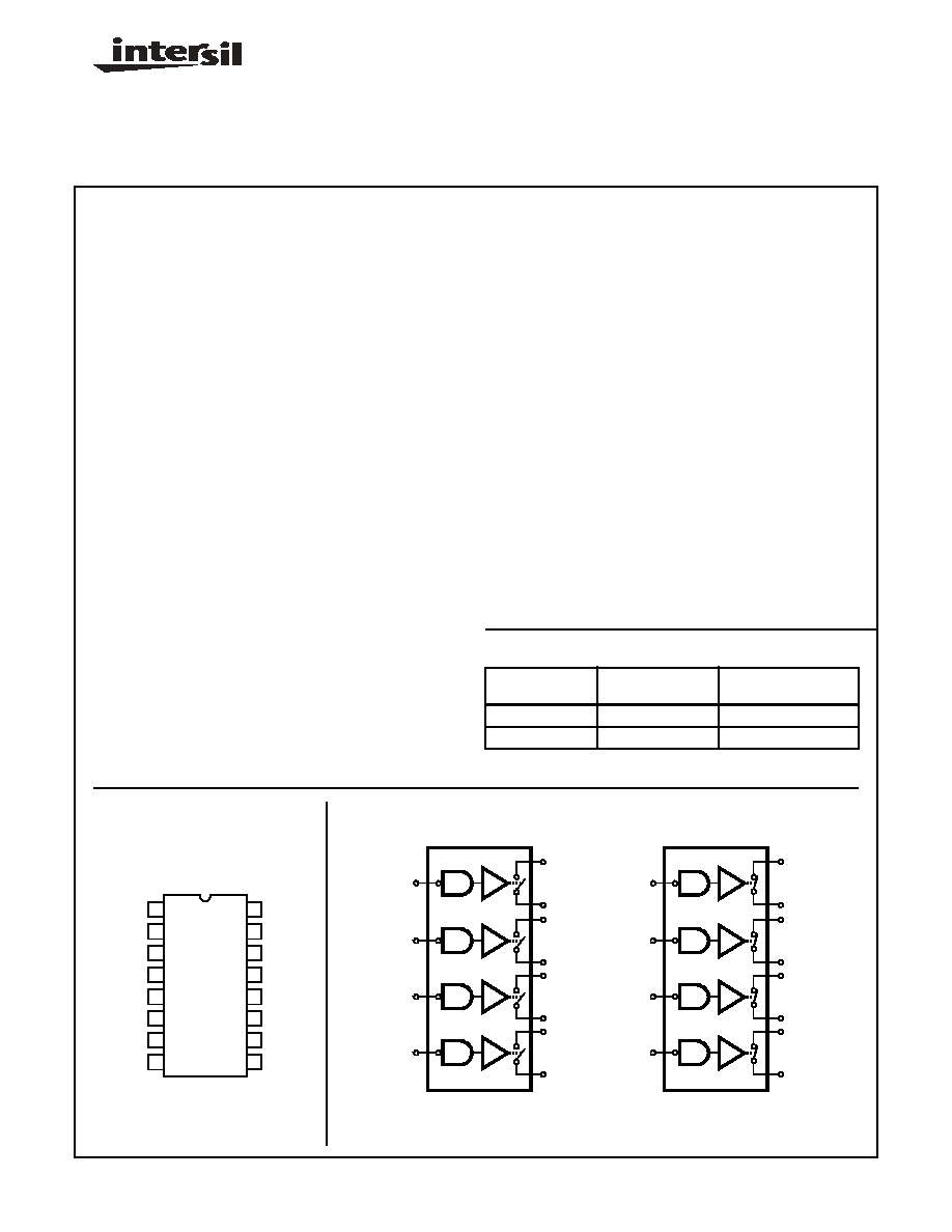
Pinout
DG441/883, DG442/883
(CERDIP)
TOP VIEW
14
15
16
9
13
12
11
10
1
2
3
4
5
7
6
8
IN
1
D
1
S
1
V-
GND
S
4
IN
4
D
4
IN
2
S
2
V+
NC
S
3
D
3
IN
3
D
2
Functional Diagrams
SWITCHES SHOWN FOR LOGIC "1" INPUT
S
1
D
1
S
2
D
2
S
3
D
3
S
4
D
4
IN
1
DG441/883
IN
2
IN
3
IN
4
IN
1
DG442/883
IN
2
IN
3
IN
4
S
1
D
1
S
2
D
2
S
3
D
3
S
4
D
4
Spec Number
512044
FN3687
CAUTION: These devices are sensitive to electrostatic discharge; follow proper IC Handling Procedures.
1-888-INTERSIL or 321-724-7143
|
Intersil (and design) is a trademark of Intersil Americas Inc.
Copyright © Intersil Americas Inc. 2002. All Rights Reserved
60
DG441/883, DG442/883
Pin Description
PIN
SYMBOL
DESCRIPTION
1
IN
1
Logic Control for Switch 1
2
D
1
Drain (Output) Terminal for Switch 1
3
S
1
Source (Input) Terminal for switch 1
4
V-
Negative Power Supply Terminal
5
GND
Ground Terminal (Logic Common)
6
S
4
Source (Input) Terminal for Switch 4
7
D
4
Drain (Output) Terminal for Switch 4
8
IN
4
Logic Control for Switch 4
9
IN
3
Logic Control for Switch 3
10
D
3
Drain (Output) Terminal for Switch 3
11
S
3
Source (Input) Terminal for Switch 3
12
NC
No Internal Connection
13
V+
Positive Power Supply Terminal (Substrate)
14
S
2
Source (Input) Terminal for Switch 2
15
D
2
Drain (Output) Terminal for Switch 2
16
IN
2
Logic Control for Switch 2
TRUTH TABLE
LOGIC
V
IN
DG441
DG442
0
0.8V
ON
OFF
1
2.4V
OFF
ON
Spec Number
512044
61
Spec Number
512044
Specifications DG441/883, DG442/883
Absolute Maximum Ratings
Thermal Information
V+ to V- . . . . . . . . . . . . . . . . . . . . . . . . . . . . . . . . . . . . . . . . . . . 44V
GND to V- . . . . . . . . . . . . . . . . . . . . . . . . . . . . . . . . . . . . . . . . . . 25V
Digital Inputs, (Note 1) . . . . . . . . . . . (V-) -2V to (V+) + 2V or 30mA,
Whichever Occurs First
Continuous Current, S or D (Note 1)
. . . . . . . . . . . . . . . . . . . . . .±
30mA
Peak Current, S or D (Note 1)
. . . . . . . . . . . . . . . . . . . . . . . . . .±
100mA
Storage Temperature Range (A Suffix) . . . . . . . . . -65
o
C to +150
o
C
Lead Temperature (Soldering 10s). . . . . . . . . . . . . . . . . . . . +300
o
C
Thermal Resistance (Max, Note 3)
JA
JC
CerDIP Package . . . . . . . . . . . . . . . . . . .
85
o
C/W
25
o
C/W
Junction Temperature . . . . . . . . . . . . . . . . . . . . . . . . . . . . . . +175
o
C
Operating Temperature (A Suffix) . . . . . . . . . . . . . . -55
o
C to +125
o
C
CAUTION: Stresses above those listed in "Absolute Maximum Ratings" may cause permanent damage to the device. This is a stress only rating and operation
of the device at these or any other conditions above those indicated in the operational sections of this specification is not implied.
Operating Conditions
Operating Voltage Range
. . . . . . . . . . . . . . . . . . . . . . . . . . . . ±
20V Max
Operating Temperature Range. . . . . . . . . . . . . . . . -55
o
C to +125
o
C
Input Low Voltage. . . . . . . . . . . . . . . . . . . . . . . . . . . . . . . . 0.8V Max
Input High Voltage. . . . . . . . . . . . . . . . . . . . . . . . . . . . . . . . 2.4V Min
Input Rise and Fall Time . . . . . . . . . . . . . . . . . . . . . . . . . . . . . . 20ns
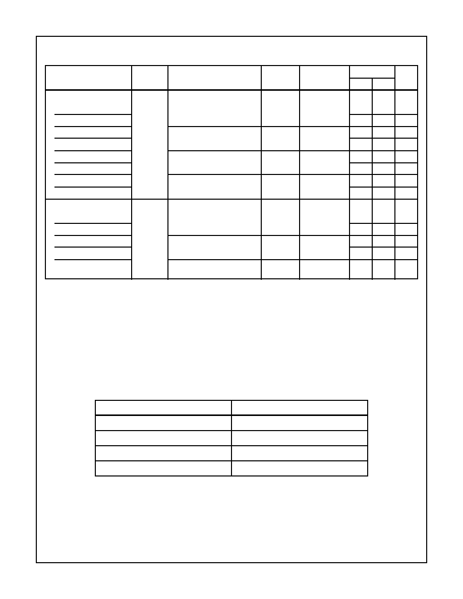
TABLE 1. DC ELECTRICAL PERFORMANCE CHARACTERISTICS
Device Tested at: -55
o
C
T
A
+125
o
C, V+ = +15V, V- = -15V, Unless Otherwise Specified
PARAMETERS
SYMBOL
CONDITIONS
GROUP A
SUBGROUP TEMPERATURE
LIMITS
UNITS
Drain-to-Source ON Resistance
R
DS(ON)
V
IN
= 0.8V
V+ = +13.5V,
V- = -13.5V,
I
S
= -10mA,
V
D
=
±
8.5V
1, 3
+25
o
C, -55
o
C
-
85
DG441/883
2
+125
o
C
-
100
DG442/883
V
IN
= 2.4V
V+ = +13.5V,
V- = -13.5V,
I
S
= -10mA,
V
D
=
±
8.5V
1, 3
+25
o
C, -55
o
C
-
85
2
+125
o
C
-
100
DG441/883
V
IN
= 0.8V
V+ = +10.8V,
V- = 0V,
I
S
= -10mA,
V
D
= 3.0V
1, 3
+25
o
C, -55
o
C
-
160
2
+125
o
C
-
200
V+ = +10.8V,
V- = 0V,
I
S
= -10mA,
V
D
= 8.0V
1, 3
+25
o
C, -55
o
C
-
160
2
+125
o
C
-
200
DG442/883
V
IN
= 2.4V
V+ = +10.8V,
V- = 0V,
I
S
= -10mA,
V
D
= 3.0V
1, 3
+25
o
C, -55
o
C
-
160
2
+125
o
C
-
200
V+ = +10.8V,
V- = 0V,
I
S
= -10mA,
V
D
= 8.0V
1, 3
+25
o
C, -55
o
C
-
160
2
+125
o
C
-
200
Source OFF Leakage Current
I
S(OFF)
V
IN
= 2.4V
V+ = +16.5V,
V- = -16.5V,
V
S
= 15.5V,
V
D
=
±
15.5V
1
+25
o
C
-0.5
0.5
nA
DG441/883
2, 3
+125
o
C, -55
o
C
-20
20
nA
DG442/883
V
IN
= 0.8V
V+ = +16.5V,
V- = -16.5V,
V
S
= 15.5V,
V
D
=
±
15.5V
1
+25
o
C
-0.5
0.5
nA
2, 3
+125
o
C, -55
o
C
-20
20
nA
62
Specifications DG441/883, DG442/883
Drain OFF Leakage Current
I
D(OFF)
V
IN
= 2.4V
V+ = +16.5V,
V- = -16.5V,
V
S
= 15.5V,
V
D
=
±
15.5V
1
+25
o
C
-0.5
0.5
nA
DG441/883
2, 3
+125
o
C, -55
o
C
-20
20
nA
DG442/883
V
IN
= 0.8V
V+ = +16.5V,
V- = -16.5V,
V
S
= 15.5V,
V
D
=
±
15.5V
1
+25
o
C
-0.5
0.5
nA
2, 3
+125
o
C, -55
o
C
-20
20
nA
Channel ON Leakage Current
I
D(ON)
+
I
S(ON)
V
IN
= 0.8V
V+ = +16.5V,
V- = -16.5V,
V
S
= V
D
=
±
15.5V
1
+25
o
C
-0.5
0.5
nA
DG441/883
2, 3
+125
o
C, -55
o
C
-40
40
nA
DG442/883
V
IN
= 2.4V
V+ = +16.5V,
V- = -16.5V,
V
S
= V
D
=
±
15.5V
1
+25
o
C
-0.5
0.5
nA
2, 3
+125
o
C, -55
o
C
-40
40
nA
Input Current with V
IN
Low
I
IL
V
IN
Under Test = 0.8V,
All Others = 2.4V
1, 2, 3
+25
o
C, +125
o
C, -
55
o
C
-0.5
0.5
µ
A
Input Current with V
IN
High
I
IH
V
IN
Under Test = 2.4V,
All Others = 0.8V
1, 2, 3
+25
o
C, +125
o
C, -
55
o
C
-0.5
0.5
µ
A
Positive Supply Current
I+
V+ = 16.5V, V- = -16.5V, V
IN
= 0V
1, 2, 3
+25
o
C, +125
o
C, -
55
o
C
-
0.1
mA
V+ = 16.5V, V- = -16.5V, V
IN
= 5V
-
0.1
mA
V+ = 13.2V, V- = 0V, V
IN
= 0V
-
0.1
mA
V+ = 13.2V, V- = 0V, V
IN
= 5V
-
0.1
mA
Negative Supply Current
I-
V+ = 16.5V, V- = -16.5V, V
IN
= 0V
1, 3
+25
o
C, -55
o
C
-1.0
-
µ
A
2
+125
o
C
-100
-
µ
A
V+ = 16.5V, V- = -16.5V, V
IN
= 5V
1, 3
+25
o
C, -55
o
C
-1.0
-
µ
A
2
+125
o
C
-100
-
µ
A
V+ = 13.2V, V- = 0V, V
IN
= 0V
1, 3
+25
o
C, -55
o
C
-1.0
-
µ
A
2
+125
o
C
-100
-
µ
A
V+ = 13.2V, V- = 0V, V
IN
= 5V
1, 3
+25
o
C, -55
o
C
-1.0
-
µ
A
2
+125
o
C
-100
-
µ
A
Ground Current
I
GND
V+ = 16.5V, V- = -16.5V, V
IN
= 0V
1, 2, 3
+25
o
C, +125
o
C, -
55
o
C
-100
-
µ
A
V+ = 16.5V, V- = -16.5V, V
IN
= 5V
-100
-
µ
A
V+ = 13.2V, V- = 0V, V
IN
= 0V
-100
-
µ
A
V+ = 13.2V, V- = 0V, V
IN
= 5V
-100
-
µ
A
TABLE 1. DC ELECTRICAL PERFORMANCE CHARACTERISTICS (Continued)
Device Tested at: -55
o
C
T
A
+125
o
C, V+ = +15V, V- = -15V, Unless Otherwise Specified
PARAMETERS
SYMBOL
CONDITIONS
GROUP A
SUBGROUP TEMPERATURE
LIMITS
UNITS
Spec Number
512044
63
Specifications DG441/883, DG442/883
TABLE 2. AC ELECTRICAL PERFORMANCE CHARACTERISTICS
Device Tested at: -55
o
C
T
A
+125
o
C, V+ = +15V, V- = -15V, Unless Otherwise Specified
PARAMETERS
SYMBOL
CONDITIONS
GROUP A
SUBGROUP TEMPERATURE
LIMITS
UNITS
MIN
MAX
Turn ON Time
t
ON
DG441
C
L
= 35pF, V
S
=
±
10V,
R
L
= 1k
9
+25
o
C
-
250
ns
DG442
-
315
ns
DG441
C
L
= 35pF, V
S
=
±
10V,
R
L
= 1k
10, 11
+125
o
C, -55
o
C
-
300
ns
DG442
-
400
ns
DG441
V+ = 12V, V- = 0V,
C
L
= 35pF, V
S
= 8.0V, R
L
= 1k
9
+25
o
C
-
400
ns
DG442
-
450
ns
DG441
V+ = 12V, V- = 0V,
C
L
= 35pF, V
S
= 8.0V, R
L
= 1k
10, 11
+125
o
C, -55
o
C
-
600
ns
DG442
-
675
ns
Turn OFF Time
t
OFF
DG441
C
L
= 35pF, V
S
=
±
10V,
R
L
= 1k
9
+25
o
C
-
120
ns
DG442
-
210
ns
DG441
C
L
= 35pF, V
S
=
±
10V,
R
L
= 1k
10, 11
+125
o
C, -55
o
C
-
150
ns
DG442
-
250
ns
DG441, DG442
V+ = 12V, V- = 0V,
C
L
= 35pF, V
S
= 8.0V, R
L
= 1k
9, 10, 11
+25
o
C, +125
o
C,
-55
o
C
-
200
ns
NOTES:
1. All leads soldered to PC Board.
2. Room: +25
o
C. Cold: A suffix -55
o
C, D suffix -40
o
C. Hot: A suffix +125
o
C, D suffix +85
o
C.
3. Dissipation rating assumes device is mounted with all leads soldered to printed circuit board.
4. Typical values are for DESIGN AID ONLY, not guaranteed nor production tested.
TABLE 3. ELECTRICAL PERFORMANCE CHARACTERISTICS
Table 3 Intentionally Left Blank.
TABLE 4. ELECTRICAL TEST REQUIREMENTS
MIL-STD-883 TEST REQUIREMENTS
SUBGROUPS (SEE TABLES 1 AND 2)
Interim Electrical Parameters (Pre Burn-In)
1
Final Electrical Test Parameters
1 (Note 1), 2, 3, 9, 10, 11
Group A Test Requirements
1, 2, 3, 9, 10, 11
Groups C and D Endpoints
1
NOTE:
1. PDA applies to Subgroup 1 only.
Spec Number
512044