 | –≠–ª–µ–∫—Ç—Ä–æ–Ω–Ω—ã–π –∫–æ–º–ø–æ–Ω–µ–Ω—Ç: EL1881CS | –°–∫–∞—á–∞—Ç—å:  PDF PDF  ZIP ZIP |
1
Æ
October 20, 2004
FN7018.1
CAUTION: These devices are sensitive to electrostatic discharge; follow proper IC Handling Procedures.
1-888-INTERSIL or 321-724-7143
|
Intersil (and design) is a registered trademark of Intersil Americas Inc.
Copyright © Intersil Americas Inc. 2002-2004. All Rights Reserved. Elantec is a registered trademark of Elantec Semiconductor, Inc.
All other trademarks mentioned are the property of their respective owners.
EL1881
Sync Separator, Low Power
The EL1881 video sync separator is manufactured using
Elantec's high performance analog CMOS process. This
device extracts sync timing information from both standard
and non-standard video input. It provides composite sync,
vertical sync, burst/back porch timing, and odd/even field
detection. Fixed 70mV sync tip slicing provides sync edge
detection when the video input level is between 0.5V
P-P
and
-2V
P-P
(sync tip amplitude 143mV to 572mV). A single
external resistor sets all internal timing to adjust for various
video standards. The composite sync output follows video in
sync pulses and a vertical sync pulse is output on the rising
edge of the first vertical serration following the vertical pre-
equalizing string. For non-standard vertical inputs, a default
vertical pulse is output when the vertical signal stays low for
longer than the vertical sync default delay time. The
odd/even output indicates field polarity detected during the
vertical blanking interval. The EL1881 is plug-in compatible
with the industry-standard LM1881 and can be substituted
for that part in 5V applications with lower required supply
current.
The EL1881 is available in the 8-pin PDIP and SO packages
and is specified for operation over the full -40∞C to +85∞C
temperature range.
Features
∑ NTSC, PAL, SECAM, non-standard video sync separation
∑ Fixed 70mV slicing of video input levels from 0.5V
P-P
to
2V
P-P
∑ Low supply current - 1.5mA typ.
∑ Single +5V supply
∑ Composite, vertical sync output
∑ Odd/even field output
∑ Burst/back porch output
∑ Available in 8-pin PDIP and SO packages
∑
Pb-free available
Applications
∑ Video amplifiers
∑ PCMCIA applications
∑ A/D drivers
∑ Line drivers
∑ Portable computers
∑ High-speed communications
∑ RGB applications
∑ Broadcast equipment
∑ Active filtering
Demo Board
A dedicated demo board is available.
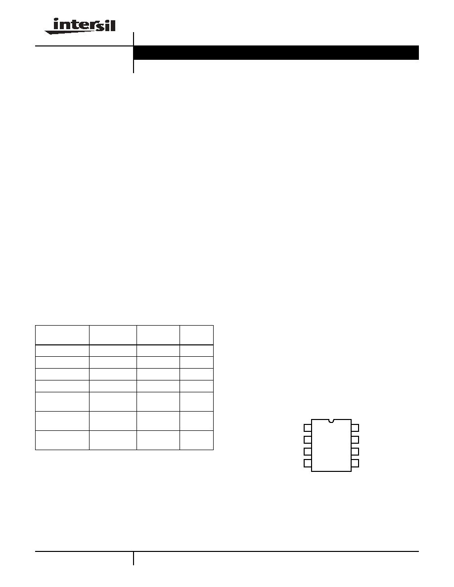
Pinout
EL1881
(8-PIN PDIP, SO)
TOP VIEW
Ordering Information
PART NUMBER
PACKAGE
TAPE & REEL
PKG.
DWG. #
EL1881CN
8-Pin PDIP
-
MDP0031
EL1881CS
8-Pin SO
-
MDP0027
EL1881CS-T7
8-Pin SO
7"
MDP0027
EL1881CS-T13
8-Pin SO
13"
MDP0027
EL1881CSZ
(See Note)
8-Pin SO
(Pb-free)
-
MDP0027
EL1881CSZ-T7
(See Note)
8-Pin SO
(Pb-free)
7"
MDP0027
EL1881CSZ-T13
(See Note)
8-Pin SO
(Pb-free)
13"
MDP0027
NOTE: Intersil Pb-free products employ special Pb-free material
sets; molding compounds/die attach materials and 100% matte tin
plate termination finish, which is compatible with both SnPb and
Pb-free soldering operations. Intersil Pb-free products are MSL
classified at Pb-free peak reflow temperatures that meet or exceed
the Pb-free requirements of IPC/JEDEC J STD-020C.
COMPOSITE SYNC OUT
COMPOSITE VIDEO IN
VERTICAL SYNC OUT
GND
V
DD
5V
ODD/EVEN OUTPUT
R
SET
BUST/BACK
PORCH OUTPUT
1
2
3
4
8
7
6
5
Data Sheet

2
FN7018.1
Absolute Maximum Ratings
(T
A
= 25∞C)
V
CC
Supply . . . . . . . . . . . . . . . . . . . . . . . . . . . . . . . . . . . . . . . . . .7V
Storage Temperature. . . . . . . . . . . . . . . . . . . . . . . .-65∞C to +150∞C
Pin Voltages. . . . . . . . . . . . . . . . . . . . . . . . . . . . -0.5V to V
CC
+0.5V
Operating Ambient Temperature Range . . . . . . . . . .-40∞C to +85∞C
Operating Junction Temperature . . . . . . . . . . . . . . . . . . . . . . . 150∞C
Power Dissipation . . . . . . . . . . . . . . . . . . . . . . . . . . . . . . . . .400mW
CAUTION: Stresses above those listed in "Absolute Maximum Ratings" may cause permanent damage to the device. This is a stress only rating and operation of the
device at these or any other conditions above those indicated in the operational sections of this specification is not implied.
IMPORTANT NOTE: All parameters having Min/Max specifications are guaranteed. Typical values are for information purposes only. Unless otherwise noted, all tests
are at the specified temperature and are pulsed tests, therefore: T
J
= T
C
= T
A
DC Electrical Specifications
V
DD
= 5V, T
A
= 25∞C, R
SET
= 681k
, unless otherwise specified.
PARAMETER
DESCRIPTION
MIN
TYP
MAX
UNIT
I
DD
, Quiescent
V
DD
= 5V
0.75
1.5
3
mA
Clamp Voltage
Pin 2, I
LOAD
= -100µA
1.35
1.5
1.65
V
Clamp Discharge Current
Pin 2 = 2V
6
12
16
µA
Clamp Charge Current
Pin 2 = 1V
-1.3
-1
0.7
mA
R
SET
Pin Reference Voltage
Pin 6
1.1
1.22
1.35
V
V
OL
Output Low Voltage
I
OL
= 1.6mA
0.24
0.5
V
V
OH
Output High Voltage
I
OH
= -40µA
4
4.8
V
I
OH
= -1.6mA
3
4.6
Dynamic Specifications
PARAMETER
DESCRIPTION
MIN
TYP
MAX
UNIT
Comp Sync Prop Delay, t
CS
See Figure 2
20
35
75
ns
Vertical Sync Width, t
VS
Normal or Default Trigger, 50%-50%
190
230
300
µs
Vertical Sync Default Delay, t
VSD
See Figure 3
35
62
85
µs
Burst/Back Porch Delay, t
BD
See Figure 2
120
200
300
ns
Burst/Back Porch Width, t
B
See Figure 2
2.5
3.5
4.5
µs
Input Dynamic Range
Video Input Amplitude to Maintain 50% Slice Spec
0.5
2
V
P-P
Slice Level
V
SLICE
/V
CLAMP
55
70
85
mV
EL1881C

3
FN7018.1
Pin Descriptions
PIN NUMBER
PIN NAME
PIN FUNCTION
1
Composite Sync
Out
Composite sync pulse output; sync pulses start on a falling edge and end on a rising edge
2
Composite Video
In
AC coupled composite video input; sync tip must be at the lowest potential (positive picture phase)
3
Vertical Sync Out
Vertical sync pulse output; the falling edge of vert sync is the start of the vertical period
4
GND
Supply ground
5
Burst/Back Porch
Output
Burst/back porch output; low during burst portion of composite video
6
RSET (Note 1)
An external resistor to ground sets all internal timing; a 681k 1% resistor will provide correct timing for
NTSC signals
7
Odd/Even Output
Odd/even field output; high during odd fields, low during even fields; transitions occur at start of vert sync
pulse
8
VDD 5V
Positive supply (5V)
NOTE:
1. R
SET
must be a 1% resistor
EL1881C

4
FN7018.1
Typical Performance Curves
Supply Current vs Temperature
R
SET
=681k
1.65
1.6
1.5
1.45
1.4
1.35
-50
-25
25
75
100
Temperature (∞C)
Supply
Current (mA)
5.5V
4.5V
5V
V
CLAMP
Voltage vs Temperature
R
SET
=681k
1.535
1.515
1.505
1.495
1.485
Temperature (∞C)
V
CLAM
P
(V
)
V
RSET
vs Temperature
R
SET
=681k
1.24
1.23
1.22
1.21
1.2
Temperature (∞C)
V
R
SET
(V
)
Clamp Charge Current vs Temperature
R
SET
=681k
1.1
1
0.9
0.85
Temperature (∞C)
Cla
m
p
Ch
arge
C
u
rr
e
n
t
(mA)
Clamp Discharge Current vs Temperature
R
SET
=681k
11.4
11.3
11.2
10.9
10.8
10.7
Temperature (∞C)
C
l
amp Di
sc
h
a
rge Curr
ent
(
µ
A)
1.525
11
1.05
0.95
1.55
0
50
-50
-25
25
75
100
0
50
-50
-25
25
75
100
0
50
-50
-25
25
75
100
0
50
-50
-25
25
75
100
0
50
5.5V
5V
4.5V
5.5V
5V
4.5V
5.5V
5V
4.5V
5.5V
4.5V
5V
11.1
1.235
1.225
1.215
1.205
R
SET
vs Horizontal Frequency
1000
600
200
0
10
15
25
35
40
45
Frequency (kHz)
R
SET
(k
)
800
400
20
30
EL1881C

5
FN7018.1
Typical Performance Curves
(Continued)
Vertical Default Delay vs R
SET
V
DD
=5V, T
A
=25∞C
120
100
60
40
20
0
200
400
600
800
1000
R
SET
(k
)
Ve
rti
c
a
l
S
y
nc De
fa
ul
t Del
a
y (µS
)
Burst/Back Porch Width vs Temperature
3.9
3.8
3.6
3.3
3.1
Temperature (∞C)
Burs
t
/
Back
Porc
h Widt
h
(
µ
S
)
Composite Sync Prop Delay vs Temperature
41
31
-50
-25
0
50
100
Temperature (∞C)
Compos
ite Sy
nc
Prop Del
ay
(
n
s
)
80
35
33
3.4
3.2
3.7
3.5
25
75
-50
-25
0
50
100
25
75
5.5V
5V
4.5V
39
37
Vertical Sync Width vs R
SET
V
DD
=5V, T
A
=25∞C
350
100
50
0
200
400
600
1000
R
SET
(k
)
Ver
t
ic
al
Sy
n
c
W
i
dt
h (µS
)
250
300
150
800
200
Burst/Back Porch Width vs R
SET
V
DD
=5V, T
A
=25∞C
6
5
4
3
2
1
200
400
600
800
1000
R
SET
(k
)
Burs
t
W
i
dth
(µS)
Burst/Back Porch Delay vs R
SET
V
DD
=5V, T
A
=25∞C
350
150
100
50
0
200
400
800
1000
R
SET
(k
)
Burst
/
Bac
k
P
o
rch De
lay
(ns
)
200
300
600
250
EL1881C