 | –≠–ª–µ–∫—Ç—Ä–æ–Ω–Ω—ã–π –∫–æ–º–ø–æ–Ω–µ–Ω—Ç: EL2075 | –°–∫–∞—á–∞—Ç—å:  PDF PDF  ZIP ZIP |
1
Æ
FN7151
CAUTION: These devices are sensitive to electrostatic discharge; follow proper IC Handling Procedures.
1-888-INTERSIL or 321-724-7143
|
Intersil (and design) is a registered trademark of Intersil Americas Inc.
Copyright © Intersil Americas Inc. 2003. All Rights Reserved. Elantec is a registered trademark of Elantec Semiconductor, Inc.
All other trademarks mentioned are the property of their respective owners.
EL2075
2GHz GBWP Gain-of-10 Stable
Operational Amplifier
The EL2075 is a precision voltage-
feedback amplifier featuring a 2GHz
gain-bandwidth product, fast settling
time, excellent differential gain and differential phase
performance, and a minimum of 50mA output current drive
over temperature.
The EL2075 is gain-of-10 stable with a -3dB bandwidth of
400MHz at A
V
= +10. It has a very low 200µV of input offset
voltage, only 2µA of input bias current, and a fully
symmetrical differential input. Like all voltage-feedback
operational amplifiers, the EL2075 allows the use of reactive
or non-linear components in the feedback loop. This
combination of speed and versatility makes the EL2075 the
ideal choice for all op-amp applications at a gain of 10 or
greater requiring high speed and precision, including active
filters, integrators, sample-and-holds, and log amps. The low
distortion, high output current, and fast settling makes the
EL2075 an ideal amplifier for signal-processing and
digitizing systems.
Features
∑ 2GHz gain-bandwidth product
∑ Gain-of-10 stable
∑ Conventional voltage-feedback topology
∑ Low offset voltage = 200µV
∑ Low bias current = 2µA
∑ Low offset current = 0.1µA
∑ Output current = 50mA over temperature
∑ Fast settling = 13ns to 0.1%
Applications
∑ Active filters/integrators
∑ High-speed signal processing
∑ ADC/DAC buffers
∑ Pulse/RF amplifiers
∑ Pin diode receivers
∑ Log amplifiers
∑ Photo multiplier amplifiers
∑ High speed sample-and-holds
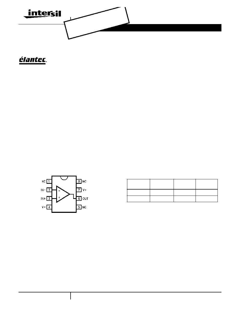
EL2075
(8-PIN SO, PDIP)
TOP VIEW
Ordering Information
PART
NUMBER
TEMP. RANGE
PACKAGE
PKG. NO.
EL2075CN
0∞C to +75∞C
8-Pin PDIP
MDP0031
EL2075CS
0∞C to +75∞C
8-Pin SO
MDP0027
Data Sheet
September 26, 2001
OBSO
LETE
PROD
UCT
NO RE
COMM
ENDE
D REP
LACE
MENT
contac
t our T
echnic
al Sup
port C
enter
at
1-888-
INTER
SIL or
www.
inters
il.com
/tsc

2
Absolute Maximum Ratings
(T
A
= 25∞C)
Supply Voltage (V
S
). . . . . . . . . . . . . . . . . . . . . . . . . . . . . . . . . . .±7V
Output Current Output is short-circuit protected to ground, however,
maximum reliability is obtained if I
OUT
does not exceed 70mA.
Common-Mode Input . . . . . . . . . . . . . . . . . . . . . . . . . . . . . . . . . ±V
S
Differential Input Voltage . . . . . . . . . . . . . . . . . . . . . . . . . . . . . . . .5V
Note: See EL2071/EL2171 for Thermal Impedance curves.
Thermal Resistance
. . . . . . . . . . . . . . . . . . . . . . . . .
JA
= 95∞C/W PDIP
. . . . . . . . . . . . . . . . . . . . . . . . . . . . . . . . . . . . . . . .
JA
= 175∞C/W SO-8
Operating Temperature . . . . . . . . . . . . . . . . . . . . . . . . 0∞C to +75∞C
Junction Temperature . . . . . . . . . . . . . . . . . . . . . . . . . . . . . . . 175∞C
Storage Temperature. . . . . . . . . . . . . . . . . . . . . . . . -60∞C to +150∞C
NOTES:
1. Measured from T
MIN
, T
MAX.
2. ±V
CC
= ±4.5V to 5.5V.
3. ±V
IN
= ±2.5V, V
OUT
= 0V.
CAUTION: Stresses above those listed in "Absolute Maximum Ratings" may cause permanent damage to the device. This is a stress only rating and operation of the
device at these or any other conditions above those indicated in the operational sections of this specification is not implied.
IMPORTANT NOTE: All parameters having Min/Max specifications are guaranteed. Typical values are for information purposes only. Unless otherwise noted, all tests
are at the specified temperature and are pulsed tests, therefore: T
J
= T
C
= T
A
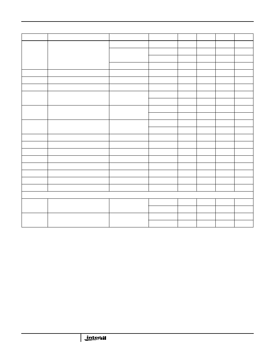
Open-Loop DC Electrical Specifications
V
S
= ±5V, R
L
= 100
, unless otherwise specified.
PARAMETER
DESCRIPTION
TEST CONDITIONS
TEMP
MIN
TYP
MAX
UNIT
V
OS
Input Offset Voltage
V
CM
= 0V
25∞C
0.2
1
mV
T
MIN
, T
MAX
2.5
mV
TCV
OS
Average Offset Voltage Drift
(Note 1)
All
8
µV/∞C
I
B
Input Bias Current
V
CM
= 0V
All
2
6
µA
I
OS
Input Offset Current
V
CM
= 0V
25∞C
0.1
1
µA
T
MIN
, T
MAX
2
µA
PSRR
Power Supply Rejection Ratio
(Note 2)
All
70
90
dB
CMRR
Common Mode Rejection Ratio
(Note 3)
All
70
90
dB
I
S
Supply Current--Quiescent
No Load
25∞C
21
25
mA
T
MIN
, T
MAX
25
mA
R
IN
(diff)
R
IN
(Differential)
Open-Loop
25∞C
15
k
C
IN
(diff)
C
IN
(Differential)
Open-Loop
25∞C
1
pF
R
IN
(cm)
R
IN
(Common-Mode)
25∞C
1
M
C
IN
(cm)
C
IN
(Common-Mode)
25∞C
1
pF
R
OUT
Output Resistance
25∞C
50
m
CMIR
Common-Mode Input
Range
25∞C
±3
±3.5
V
T
MIN
, T
MAX
±2.5
V
I
OUT
Output Current
All
50
70
mA
V
OUT
Output Voltage Swing
No Load
All
±3.5
±4
V
V
OUT
100
Output Voltage Swing
100
All
±3
±3.6
V
V
OUT
50
Output Voltage Swing
50
All
±2.5
±3.4
V
A
VOL
100
Open-Loop Gain
100
25∞C
1000
2800
V/V
T
MIN
, T
MAX
800
V/V
A
VOL
50
Open-Loop Gain
50
25∞C
800
2300
V/V
T
MIN
, T
MAX
600
V/V
e
N
@ > 1MHz
Noise Voltage 1≠100MHz
25∞C
2.3
nV/
Hz
i
N
@ > 100kHz
Noise Current 100k≠100MHz
25∞C
3.2
pA/
Hz
EL2075
3
NOTES:
1. Large-signal bandwidth calculated using LSBW = Slew Rate (2
*
V
PEAK
)
.
2. All distortion measurements are made with V
OUT
= 2V
PP
, R
L
= 100
.
Closed-Loop AC Electrical Specifications
V
S
= ±5V, A
V
= +20, R
F
= 1500
, R
L
= 100
unless otherwise specified.
PARAMETER
DESCRIPTION
TEST CONDITIONS
TEMP
MIN
TYP
MAX
UNIT
SSBW
-3dB Bandwidth
(V
OUT
= 0.4V
PP
)
A
V
= +10
25∞C
400
MHz
A
V
= +20
25∞C
150
200
MHz
T
MIN
, T
MAX
125
MHz
A
V
= +50
25∞C
40
MHz
GBWP
Gain-Bandwidth Product
A
V
= +100
25∞C
2.0
GHz
LSBWa
-3dB Bandwidth
V
OUT
= 2V
PP
(Note 1)
All
80
128
MHz
LSBWb
-3dB Bandwidth
V
OUT
= 5V
PP
(Note 1)
All
32
50
MHz
GFPL
Peaking (< 50MHz)
V
OUT
= 0.4V
PP
25∞C
0
0.5
dB
T
MIN
, T
MAX
0.5
dB
GFPH
Peaking (> 50MHz)
V
OUT
= 0.4V
PP
25∞C
0
1
dB
T
MIN
, T
MAX
1
dB
GFR
Rolloff (< 100MHz)
V
OUT
= 0.4V
PP
25∞C
0.1
0.5
dB
T
MIN
, T
MAX
0.5
dB
LPD
Linear Phase Deviation (< 100MHz)
V
OUT
= 0.4V
PP
All
1
1.8
∞
PM
Phase Margin
A
V
= +10
25∞C
60
∞
t
R
1, t
F
1
Rise Time, Fall Time
0.4V Step, A
V
= +10
25∞C
1.2
ns
t
R
2, t
F
2
Rise Time, Fall Time
5V Step, A
V
= +10
25∞C
6
ns
t
S
1
Settling to 0.1% (A
V
= -20)
2V Step
25∞C
13
ns
t
S
2
Settling to 0.01% (A
V
= -20)
2V Step
25∞C
25
ns
OS
Overshoot
2V Step, A
V
= +10
25∞C
10
%
SR
Slew Rate
2V Step, A
V
= +10
All
500
800
V/µs
DISTORTION (Note 2)
HD2
2nd Harmonic Distortion
@ 20MHz, A
V
= +20
25∞C
-40
-30
dBc
T
MIN
, T
MAX
-30
dBc
HD3
3rd Harmonic Distortion
@ 20MHz, A
V
= +20
25∞C
-65
-50
dBc
T
MIN
, T
MAX
-50
dBc
EL2075

4
Typical Performance Curves
Non-Inverting
Frequency Response
Inverting Frequency Response
Frequency Response
for Various R
L
s
Equivalent Input Noise
Output Voltage Swing
vs Frequency
Open Loop Gain
and Phase
PSRR, CMRR, and Closed-Loop
R
O
Frequency
2nd and 3rd Harmonic
Distortion vs Frequency
2-Tone, 3rd Order
Intermodulation Intercept
EL2075

5
Typical Performance Curves
(Continued)
Series Resistor and Resulting
Bandwidth vs Capacitive Load
Settling Time vs
Output Voltage Change
Settling Time vs
Closed-Loop Gain
Supply Current
vs Temperature
Bias and Offset Current vs
Input Common-Mode Voltage
Common-Mode Rejection
Ratio vs Input Common-Mode
Voltage
Bias and Offset Current
vs Temperature
Offset Voltage
vs Temperature
A
VOL
, PSRR, and CMRR
vs Temperature
Small Signal Transient Response
Large Signal Transient Response
EL2075