 | –≠–ª–µ–∫—Ç—Ä–æ–Ω–Ω—ã–π –∫–æ–º–ø–æ–Ω–µ–Ω—Ç: EL2120CN | –°–∫–∞—á–∞—Ç—å:  PDF PDF  ZIP ZIP |

1
Æ
FN7044
CAUTION: These devices are sensitive to electrostatic discharge; follow proper IC Handling Procedures.
1-888-INTERSIL or 321-724-7143
|
Intersil (and design) is a registered trademark of Intersil Americas Inc.
Copyright © Intersil Americas Inc. 2003. All Rights Reserved. Elantec is a registered trademark of Elantec Semiconductor, Inc.
All other trademarks mentioned are the property of their respective owners.
EL2120
100MHz Current Feedback Amplifier
The EL2120 is a wideband current
feedback amplifier optimized for video
performance. Its 0.01% differential
gain and 0.03 degree differential phase performance when
at ±5V supplies exceeds the performance of other amplifiers
running on ±15V supplies. Operating on ±8 to ±15V supplies
reduces distortions to 0.01% and 0.01 degrees and below.
The EL2120 can operate with supplies as low as ±2.5V or a
single +5V supply.
Being a current feedback design, bandwidth is a relatively
constant 100MHz over the ±1 to ±10 gain range. The
EL2120 has been optimized for flat gain over frequency and
all characteristics are maintained at positive unity gain.
Because the input slew rate is similar to the 700V/µs output
slew rate the part makes an excellent high-speed buffer.
The EL2120 has a superior output disable function. Time to
enable or disable is 50ns and does not change markedly
with temperature. Furthermore, in disable mode the output
does not draw excessive currents when driven with
1000V/µs slew rates. The output appears as a 3pF load
when disabled.
Simplified Schematic
Features
∑ Excellent differential gain and phase on ±5V to ±15V
supplies
∑ 100MHz -3dB bandwidth from gains of ±1 to ±10
∑ 700V/µs slew rate
∑ 0.1dB flatness to 20MHz
∑ Output disable in 50ns - remains high impedance even
when driven with large slew rates
∑ Single +5V supply operation
∑ AC characteristics are lot and temperature stable
∑ Available in small SO-8 package
Applications
∑ Video gain block
∑ Residue amplifier
∑ Multiplexer
∑ Current to voltage converter
∑ Coax cable driver with gain of 2
∑ ADC driver
Pinouts
Ordering Information
PART
NUMBER
TEMP. RANGE
PACKAGE
PKG. NO.
EL2120CN
0∞C to +75∞C
8-Pin PDIP
MDP0031
EL2120CS
0∞C to +75∞C
8-Pin SO
MDP0027
EL2120
(8-PIN PDIP)
TOP VIEW
EL2120
(8-PIN SO)
TOP VIEW
Data Sheet
January 1996, Rev E
2
NOTES:
1. The input is moved from -3V to +3V
2. The supplies are moved from ±5V to ±15V
Absolute Maximum Ratings
(T
A
= 25∞C)
Voltage between V+ and V- . . . . . . . . . . . . . . . . . . . . . . . . . . . . .33V
Voltage at +IN, -IN, V
OUT
. . . . . . . . . . . . . (V-) - 0.5V to (V+) + 0.5V
Voltage between +IN and -IN . . . . . . . . . . . . . . . . . . . . . . . . . . . .±5V
Voltage at /Disable . . . . . . . . . . . . . . . . . . . (V+) - 10V to (V+) + 0.5V
Current into +IN, -IN, and /Disable. . . . . . . . . . . . . . . . . . . . . . ±5mA
Output Current . . . . . . . . . . . . . . . . . . . . . . . . . . . . . . . . . . . . ±50mA
Internal Power Dissipation . . . . . . . . . . . . . . . . . . . . . . . See Curves
Operating Ambient Temperature Range . . . . . . . . . . . . . .0∞ to 75∞C
Operating Junction Temperature PDIP or SO . . . . . . . . . . . . . 150∞C
Storage Temperature Range . . . . . . . . . . . . . . . . . . -65∞C to +150∞C
CAUTION: Stresses above those listed in "Absolute Maximum Ratings" may cause permanent damage to the device. This is a stress only rating and operation of the
device at these or any other conditions above those indicated in the operational sections of this specification is not implied.
IMPORTANT NOTE: All parameters having Min/Max specifications are guaranteed. Typical values are for information purposes only. Unless otherwise noted, all tests
are at the specified temperature and are pulsed tests, therefore: T
J
= T
C
= T
A
Open-Loop DC Electrical Specifications
V
S
= ±5V; R
L
= 150
, T
A
= 25∞C unless otherwise specified
PARAMETER
DESCRIPTION
TEMP
MIN
TYP
MAX
UNITS
V
OS
Input Offset Voltage
V
S
= ±15V
Full
Full
4
2
20
25
mV
mV
V
OS
/T
Input Offset Drift
Full
20
µV/∞C
I
B+
+V
IN
Input Bias Current
Full
5
15
µA
I
B-
-V
IN
Input Bias Current
Full
10
50
µA
CMRR
Common-Mode Rejection (Note 1)
Full
50
55
dB
-ICMR
-Input Current Common-Mode Rejection (Note 1)
Full
8
20
µA/V
PSRR
Power Supply Rejection (Note 2)
Full
65
80
dB
+IPSR
+Input Current Power Supply Rejection (Note 2)
25∞C
0.03
µA/V
-IPSR
-Input Current Power Supply Rejection (Note 2)
Full
0.6
5
µA/V
R
OL
Transimpedance
Full
70
140
k
A
VOL
Voltage Gain
Full
58
66
dB
+R
IN
+V
IN
Input Impedance
25∞C
2
M
V
IN
+V
IN
Range
Full
±3.0
±3.5
V
V
O
Output Voltage Swing
Full
±3.0
±3.5
V
I
SC
Output Short-Circuit Current
25∞C
100
mA
I
O,DIS
Output Current, Disabled
Full
5
50
µA
V
DIS,ON
Disable Pin Voltage for Output Enabled
Full
(V+) - 1
V
V
DIS,OFF
Disable Pin Voltage for Output Disabled
Full
(V+) - 4
V
I
DIS,ON
Disable Pin Current for Output Enabled
Full
5
µA
I
DIS,OFF
Disable Pin Current for Output Disabled
Full
1.0
mA
I
S
Supply Current (V
S
= ±15V)
Full
17
20
mA
EL2120

3
Typical Performance Curves
Closed-Loop AC Electrical Specifications
V
S
= ±15V; A
V
= +2 (R
F
= R
G
= 270
); R
L
= 150
; C
L
= 7pF; C
IN-
= 2pF; T
A
= 25∞C
PARAMETER
DESCRIPTION
MIN
TYP
MAX LEVEL
UNITS
SR
Slew Rate; V
OUT
from -3V to +3V
Measured at -2V and +2V
V
S
= ±15V
V
S
= ±5V
750
550
V/µs
V/µs
t
S
Settling Time to 0.25% of a
0 to +10V Swing; A
V
= +1 with
R
F
= 270
, R
G
= ◊, and R
L
= 400
50
ns
BW
Bandwidth -3dB
±1dB
±0.1dB
95
50
16
MHz
MHz
MHz
BW@2.5V
Bandwidth at -3dB
V
S
= ±2.5V ±1dB
±0.1dB
75
35
11
MHz
MHz
MHz
Peaking
0.5
dB
dG
Differential Gain; DC Offset
from -0.7V through +0.7V, AC
Amplitude 286 mVp≠p
V
S
= ±15V, f = 3.58MHz
V
S
= ±15V, f = 30MHz
V
S
= ±5V, f = 3.58MHz
<0.01
0.1
0.01
%
%
%
d
Differential Phase; DC Offset
from -0.7V through +0.7V, AC
Amplitude 286 mVp≠p
V
S
= ±15V, f = 3.58MHz
V
S
= ±15V, f = 30MHz
V
S
= ±5V, f = 3.58MHz
0.01
0.1
0.06
∞
∞
∞
AC Test Circuit
Frequency Response vs R
F
Frequency Response vs Gain
Frequency Response vs Load
EL2120

4
Typical Performance Curves
(Continued)
Gain Flatness vs R
F
Gain Flatness vs C
IN
-
-3dB Bandwidth, 0.1dB Bandwidth,
and Peaking vs Temperature
at V
S
±15V
-3dB Bandwidth, 0.1dB Bandwidth,
and Peaking vs Temperature
at V
S
±5V
-3dB Bandwidth, 0.1dB Bandwidth,
and Peaking vs Supply Voltage
Deviation From Linear
Phase vs Frequency
EL2120
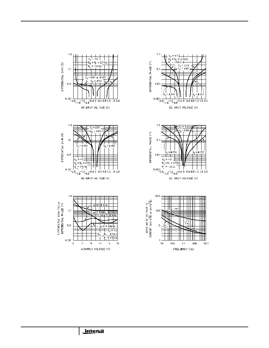
5
Typical Performance Curves
(Continued)
Differential Gain vs
DC Input Offset
at 3.58MHz
Differential Phase vs
DC Input Offset
at 3.58MHz
Differential Phase vs
DC Input Offset
at 30MHz
Differential Gain vs
DC Input Offset
at 30MHz
Input Noise Voltage
and Current
Differential Gain and Phase
vs Supply Voltage
(V
IN
, DC from 0 to +0.7V)
EL2120