
1
ģ
FN7046.2
EL2126
Ultra-Low Noise, Low Power, Wideband
Amplifier
The EL2126 is an ultra-low noise, wideband amplifier that
runs on half the supply current of competitive parts. It is
intended for use in systems such as ultrasound imaging
where a very small signal needs to be amplified by a large
amount without adding significant noise. Its low power
dissipation enables it to be packaged in the tiny SOT-23
package, which further helps systems where many input
channels create both space and power dissipation problems.
The EL2126 is stable for gains of 10 and greater and uses
traditional voltage feedback. This allows the use of reactive
elements in the feedback loop, a common requirement for
many filter topologies. It operates from Ī2.5V to Ī15V
supplies and is available in the 5-pin SOT-23 and 8-pin SO
packages.
The EL2126 is fabricated in Elantec's proprietary
complementary bipolar process, and is specified for
operation over the full -40įC to +85įC temperature range.
Pinouts
EL2126
(5-PIN SOT-23)
TOP VIEW
EL2126
(8-PIN SO)
TOP VIEW
Features
∑ Voltage noise of only 1.3nV/
Hz
∑ Current noise of only 1.2pA/
Hz
∑ 200ĶV offset voltage
∑ 100MHz -3dB BW for A
V
= 10
∑ Very low supply current - 4.7mA
∑ SOT-23 package
∑ Ī2.5V to Ī15V operation
∑
Pb-Free available (RoHS compliant)
Applications
∑ Ultrasound input amplifiers
∑ Wideband instrumentation
∑ Communication equipment
∑ AGC & PLL active filters
∑ Wideband sensors
1
2
3
5
4
-
+
VS+
IN-
IN+
VS-
OUT
1
2
3
4
8
7
6
5
-
+
NC
IN-
IN+
VS-
NC
VS+
OUT
NC
Ordering Information
PART NUMBER
PACKAGE
TAPE & REEL PKG. DWG. #
EL2126CW-T7
5-Pin SOT-23
7" (3K pcs)
MDP0038
EL2126CW-T7A
5-Pin SOT-23
7" (250 pcs)
MDP0038
EL2126CS
8-Pin SO
-
MDP0027
EL2126CS-T7
8-Pin SO
7"
MDP0027
EL2126CS-T13
8-Pin SO
13"
MDP0027
EL2126CSZ
(See Note)
8-Pin SO
(Pb-free)
-
MDP0027
EL2126CSZ-T7
(See Note)
8-Pin SO
(Pb-free)
7"
MDP0027
EL2126CSZ-T13
(See Note)
8-Pin SO
(Pb-free)
13"
MDP0027
NOTE: Intersil Pb-free products employ special Pb-free material sets;
molding compounds/die attach materials and 100% matte tin plate
termination finish, which are RoHS compliant and compatible with
both SnPb and Pb-free soldering operations. Intersil Pb-free products
are MSL classified at Pb-free peak reflow temperatures that meet or
exceed the Pb-free requirements of IPC/JEDEC J STD-020.
Data Sheet
May 9, 2005
CAUTION: These devices are sensitive to electrostatic discharge; follow proper IC Handling Procedures.
1-888-INTERSIL or 1-888-352-6832
|
Intersil (and design) is a registered trademark of Intersil Americas Inc.
Copyright Intersil Americas Inc. 2004, 2005. All Rights Reserved
All other trademarks mentioned are the property of their respective owners.

2
Absolute Maximum Ratings
(T
A
= 25įC)
V
S
+ to V
S
- . . . . . . . . . . . . . . . . . . . . . . . . . . . . . . . . . . . . . . . . . .33V
Continuous Output Current . . . . . . . . . . . . . . . . . . . . . . . . . . . 40mA
Any Input . . . . . . . . . . . . . . . . . . . . . . . . . . V
S
+ - 0.3V to V
S
- + 0.3V
Power Dissipation . . . . . . . . . . . . . . . . . . . . . . . . . . . . . See Curves
Operating Temperature . . . . . . . . . . . . . . . . . . . . . . .-40įC to +85įC
Storage Temperature . . . . . . . . . . . . . . . . . . . . . . . . -60įC to +150įC
Maximum Die Junction Temperature . . . . . . . . . . . . . . . . . . . +150įC
CAUTION: Stresses above those listed in "Absolute Maximum Ratings" may cause permanent damage to the device. This is a stress only rating and operation of the
device at these or any other conditions above those indicated in the operational sections of this specification is not implied.
IMPORTANT NOTE: All parameters having Min/Max specifications are guaranteed. Typical values are for information purposes only. Unless otherwise noted, all tests
are at the specified temperature and are pulsed tests, therefore: T
J
= T
C
= T
A
Electrical Specifications
V
S
+ = +5V, V
S
- = -5V, T
A
= 25įC, R
F
= 180
, R
G
= 20
, R
L
= 500
unless otherwise specified.
PARAMETER
DESCRIPTION
CONDITIONS
MIN
TYP
MAX
UNIT
DC PERFORMANCE
V
OS
Input Offset Voltage (SO8)
0.2
2
mV
Input Offset Voltage (SOT23-5)
3
mV
T
CVOS
Offset Voltage Temperature
Coefficient
17
ĶV/įC
I
B
Input Bias Current
-10
-7
ĶA
I
OS
Input Bias Current Offset
0.06
0.6
ĶA
T
CIB
Input Bias Current Temperature
Coefficient
0.013
ĶA/įC
C
IN
Input Capacitance
2.2
pF
A
VOL
Open Loop Gain
V
O
= -2.5V to +2.5V
80
87
dB
PSRR
Power Supply Rejection Ratio
(Note 1)
80
100
dB
CMRR
Common Mode Rejection Ratio
at CMIR
75
106
dB
CMIR
Common Mode Input Range
-4.6
3.8
V
V
OUTH
Positive Output Voltage Swing
No load, R
F
= 1k
3.8
3.8
V
V
OUTL
Negative Output Voltage Swing
No load, R
F
= 1k
-4
-3.9
V
V
OUTH2
Positive Output Voltage Swing
R
L
= 100
3.2
3.45
V
V
OUTL2
Negative Output Voltage Swing
R
L
= 100
-3.5
-3.2
V
I
OUT
Output Short Circuit Current
(Note 2)
80
100
mA
I
SY
Supply Current
4.7
5.5
mA
AC PERFORMANCE - R
G
= 20
, C
L
= 3pF
BW
-3dB Bandwidth, R
L
= 500
100
MHz
BW Ī0.1dB
Ī0.1dB Bandwidth, R
L
= 500
17
MHz
BW Ī1dB
Ī1dB Bandwidth, R
L
= 500
80
MHz
Peaking
Peaking, R
L
= 500
0.6
dB
SR
Slew Rate
V
OUT
= 2V
PP
, measured at 20% to 80%
80
110
V/Ķs
OS
Overshoot, 4Vpk-pk Output Square
Wave
Positive
2.8
%
Negative
-7
%
t
S
Settling Time to 0.1% of Ī1V Pulse
51
ns
V
N
Voltage Noise Spectral Density
1.3
nV/
Hz
I
N
Current Noise Spectral Density
1.2
pA/
Hz
EL2126

3
HD2
2nd Harmonic Distortion (Note 3)
-70
dBc
HD3
3rd Harmonic Distortion (Note 3)
-70
dBc
NOTES:
1. Measured by moving the supplies from Ī4V to Ī6V
2. Pulse test only and using a 10
load
3. Frequency = 1MHz, V
OUT
= 2Vpk-pk, into 500
and 5pF load
Electrical Specifications
V
S
+ = +5V, V
S
- = -5V, T
A
= 25įC, R
F
= 180
, R
G
= 20
, R
L
= 500
unless otherwise specified. (Continued)
PARAMETER
DESCRIPTION
CONDITIONS
MIN
TYP
MAX
UNIT
Electrical Specifications
V
S
+ = +15V, V
S
- = -15V, T
A
= 25įC, R
F
= 180
, R
G
= 20
, R
L
= 500
unless otherwise specified.
PARAMETER
DESCRIPTION
CONDITIONS
MIN
TYP
MAX
UNIT
DC PERFORMANCE
V
OS
Input Offset Voltage (SO8)
0.5
3
mV
Input Offset Voltage (SOT23-5)
3
mV
T
CVOS
Offset Voltage Temperature
Coefficient
4.5
ĶV/įC
I
B
Input Bias Current
-10
-7
ĶA
I
OS
Input Bias Current Offset
0.12
0.7
ĶA
T
CIB
Input Bias Current Temperature
Coefficient
0.016
ĶA/įC
C
IN
Input Capacitance
2.2
pF
A
VOL
Open Loop Gain
80
90
dB
PSRR
Power Supply Rejection Ratio
(Note 1)
65
80
dB
CMRR
Common Mode Rejection Ratio
at CMIR
70
85
dB
CMIR
Common Mode Input Range
-14.6
13.8
V
V
OUTH
Positive Output Voltage Swing
No load, R
F
= 1k
13.6
13.7
V
V
OUTL
Negative Output Voltage Swing
No load, R
F
= 1k
-13.8
-13.7
V
V
OUTH2
Positive Output Voltage Swing
R
L
= 100
, R
F
= 1k
10.2
11.2
V
V
OUTL2
Negative Output Voltage Swing
R
L
= 100
, R
F
= 1k
-10.3
-9.5
V
I
OUT
Output Short Circuit Current
(Note 2)
140
220
mA
I
SY
Supply Current
5
6
mA
AC PERFORMANCE - R
G
= 20
, C
L
= 3pF
BW
-3dB Bandwidth, R
L
= 500
135
MHz
BW Ī0.1dB
Ī0.1dB Bandwidth, R
L
= 500
26
MHz
BW Ī1dB
Ī1dB Bandwidth, R
L
= 500
60
MHz
Peaking
Peaking, R
L
= 500
2.1
dB
SR
Slew Rate (Ī2.5V Square Wave,
Measured 25%-75%)
130
150
V/ĶS
OS
Overshoot, 4Vpk-pk Output Square
Wave
Positive
1.6
%
Negative
-4.4
%
T
S
Settling Time to 0.1% of Ī1V Pulse
48
ns
V
N
Voltage Noise Spectral Density
1.4
nV/
Hz
EL2126

4
NOTES:
1. Measured by moving the supplies from Ī13.5V to Ī16.5V
2. Pulse test only and using a 10
load
3. Frequency = 1MHz, V
OUT
= 2Vpk-pk, into 500
and 5pF load
I
N
Current Noise Spectral Density
1.1
pA/
Hz
HD2
2nd Harmonic Distortion (Note 3)
-72
dBc
HD3
3rd Harmonic Distortion (Note 3)
-73
dBc
Electrical Specifications
V
S
+ = +15V, V
S
- = -15V, T
A
= 25įC, R
F
= 180
, R
G
= 20
, R
L
= 500
unless otherwise specified.
(Continued)
PARAMETER
DESCRIPTION
CONDITIONS
MIN
TYP
MAX
UNIT
EL2126
5
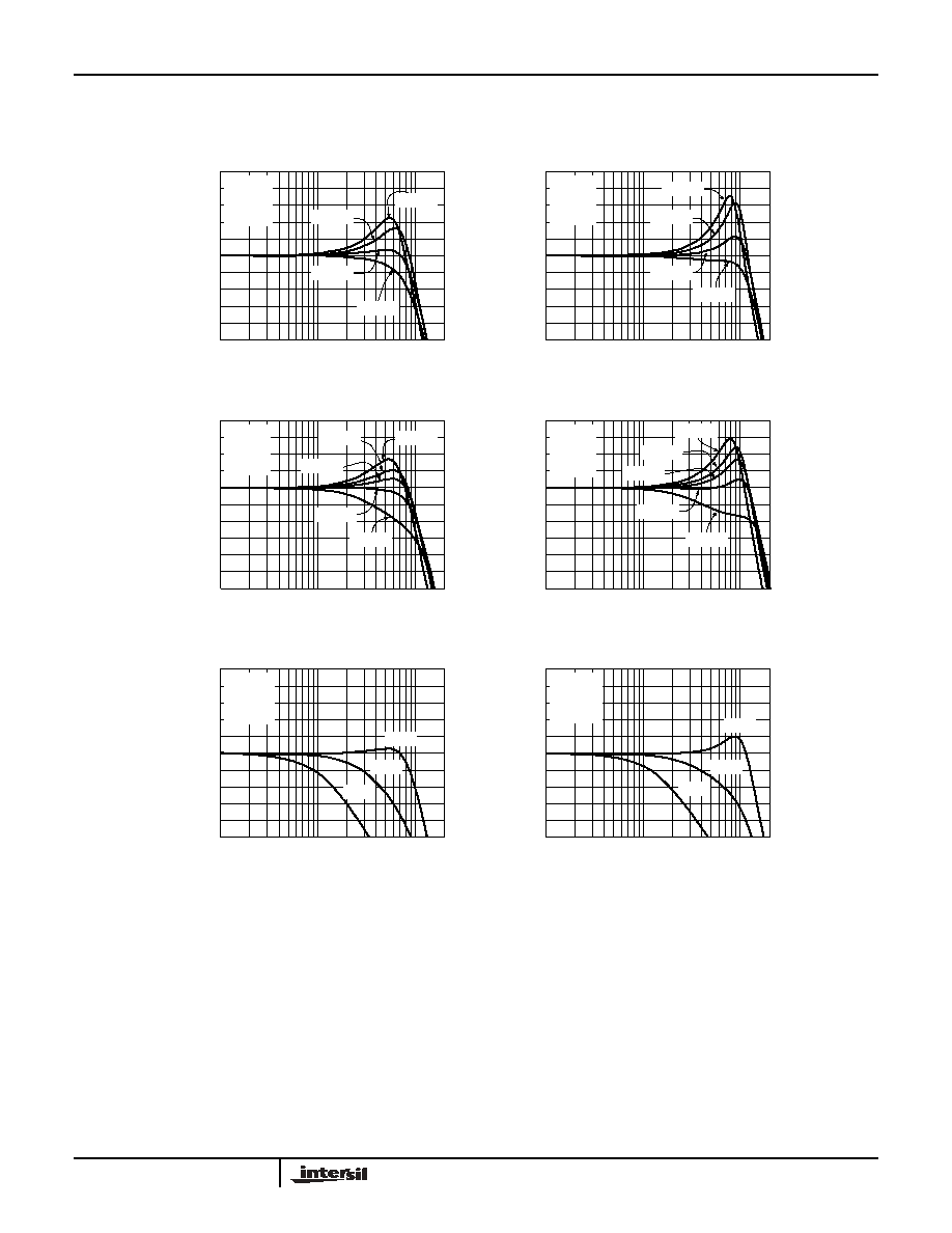
Typical Performance Curves
Non-Inverting Frequency Response for Various R
F
10
6
2
-2
-6
-10
1M
10M
100M
Frequency (Hz)
Norma
liz
ed Gain (dB)
R
F
=1k
R
F
=500
R
F
=180
R
F
=100
V
S
=Ī5V
A
V
=10
C
L
=5pF
R
L
=500
Non-Inverting Frequency Response for Various R
F
10
6
2
-2
-6
-10
1M
10M
100M
Frequency (Hz)
Norma
liz
ed Gain (dB)
R
F
=1k
R
F
=500
R
F
=180
R
F
=100
Inverting Frequency Response for Various R
F
8
4
0
-4
-8
-12
1M
10M
100M
Frequency (Hz)
No
r
m
ali
z
ed Ga
in (dB)
V
S
=Ī15V
A
V
=-10
C
L
=5pF
R
L
=500
Inverting Frequency Response for Various R
F
8
4
0
-4
-8
-12
1M
10M
100M
Frequency (Hz)
No
r
m
ali
z
ed Ga
in (dB)
V
S
=Ī5V
A
V
=-10
C
L
=5pF
R
L
=500
Non-Inverting Frequency Response for Various Gain
10
6
2
-2
-6
-10
1M
10M
100M
Frequency (Hz)
Norma
liz
e
d
Gai
n
(d
B)
A
V
=10
V
S
=Ī5V
R
G
=20
R
L
=500
C
L
=5pF
Non-Inverting Frequency Response for Various Gain
10
6
2
-2
-6
-10
1M
10M
100M
Frequency (Hz)
Norma
liz
e
d
Gai
n
(d
B)
R
F
=1k
R
F
=350
R
F
=100
R
F
=200
R
F
=500
R
F
=1k
R
F
=500
R
F
=200
R
F
=100
R
F
=350
A
V
=20
A
V
=50
V
S
=Ī15V
R
G
=20
R
L
=500
C
L
=5pF
A
V
=10
A
V
=20
A
V
=50
V
S
=Ī15V
A
V
=10
C
L
=5pF
R
L
=500
EL2126