 | –≠–ª–µ–∫—Ç—Ä–æ–Ω–Ω—ã–π –∫–æ–º–ø–æ–Ω–µ–Ω—Ç: EL4340IUZ | –°–∫–∞—á–∞—Ç—å:  PDF PDF  ZIP ZIP |
1
Æ
FN7421.1
CAUTION: These devices are sensitive to electrostatic discharge; follow proper IC Handling Procedures.
1-888-INTERSIL or 1-888-468-3774
|
Intersil (and design) is a registered trademark of Intersil Americas Inc.
Copyright © Intersil Americas Inc. 2005. All Rights Reserved.
All other trademarks mentioned are the property of their respective owners.
EL4340, EL4342
500MHz Triple, Multiplexing Amplifiers
The EL4340 and EL4342 are fixed unity gain mux amps
featuring high slew rates and excellent bandwidth for video
switching. These devices feature a high impedance output
state (HIZ) that enables the outputs of multiple devices to be
wired together. A power-down mode (ENABLE) is included
to turn off un-needed circuitry in power sensitive
applications. The ENABLE pin, when pulled high, sets the
EL4340 and EL4342 into standby power mode - consuming
just 18mW. An added feature in the EL4340 is a latch enable
function (LE) that allows independent logic control using a
common logic bus.
Features
∑ Triple 2:1 and 4:1 multiplexers for RGB
∑ Internally set gain-of-1
∑ High speed three-state outputs (HIZ)
∑ Power-down mode (ENABLE)
∑ Latch enable (EL4340)
∑ ±5V operation
∑ ±870 V/µs slew rate
∑ 500MHz bandwidth
∑ Supply current 11mA/ch (EL4340) and 16mA/ch (EL4342)
∑ Pb-free plus anneal available (RoHS compliant)
Applications
∑ HDTV/DTV analog inputs
∑ Video projectors
∑ Computer monitors
∑ Set-top boxes
∑ Security video
∑ Broadcast video equipment
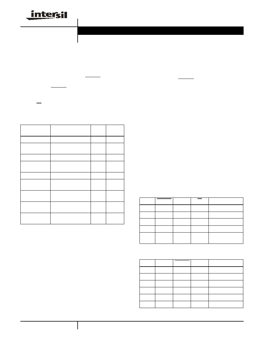
Ordering Information
PART NUMBER
PACKAGE
TAPE &
REEL
PKG.
DWG. #
EL4340IU
24 Ld QSOP
-
MDP0040
EL4340IUZ
(See Note)
24 Ld QSOP (Pb-free)
-
MDP0040
EL4340IU-T7
24 Ld QSOP
7"
MDP0040
EL4340IUZ-T7
(See Note)
24 Ld QSOP (Pb-free)
7"
MDP0040
EL4340IU-T13
24 Ld QSOP
13"
MDP0040
EL4340IUZ-T13
(See Note)
24 Ld QSOP (Pb-free)
13"
MDP0040
EL4342ILZA
(See Note)
32 Ld Exposed Pad
3.6 x 4.6 QFN (Pb-free)
-
MDP0046
EL4342ILZA-T7
(See Note)
32 Ld Exposed Pad
3.6 x 4.6 QFN (Pb-free)
7"
MDP0046
EL4342ILZA-T13
(See Note)
32 Ld Exposed Pad
3.6 x 4.6 QFN (Pb-free)
13"
MDP0046
NOTE: Intersil Pb-free plus anneal products employ special Pb-free
material sets; molding compounds/die attach materials and 100%
matte tin plate termination finish, which are RoHS compliant and
compatible with both SnPb and Pb-free soldering operations. Intersil
Pb-free products are MSL classified at Pb-free peak reflow
temperatures that meet or exceed the Pb-free requirements of
IPC/JEDEC J STD-020.
TABLE 1. CHANNEL SELECT LOGIC TABLE EL4340
S0
ENABLE
HIZ
LE
OUTPUT
0
0
0
0
INO (A, B, C)
1
0
0
0
IN1 (A, B, C)
X
1
X
X
Power-down
X
0
1
X
High Z
X
0
0
1
Last S0 State
Preserved
TABLE 2. CHANNEL SELECT LOGIC TABLE EL4342
S1
S0
ENABLE
HIZ
OUTPUT
0
0
0
0
IN0 (A, B, C)
0
1
0
0
IN1 (A, B, C)
1
0
0
0
IN2 (A, B, C)
1
1
0
0
IN3 (A, B, C)
X
X
1
X
Power-down
X
X
0
1
High Z
Data Sheet
September 21, 2005

2
FN7421.1
September 21, 2005
Pinouts
EL4340
(24 LD QSOP)
TOP VIEW
EL4342
(32 LD QFN)
TOP VIEW
Functional Diagram EL4340
Functional Diagram EL4342
GND B
NIC
GND A
IN0A
IN0B
NIC
LE
ENABLE
HIZ
OUTA
NIC
IN0C
V+
OUTB
1
2
3
4
16
15
14
13
5
6
7
12
11
9
8
10
20
19
18
17
24
23
22
21
IN1B
NIC
IN1A
OUTC
V-
NIC
IN1C
GND C
S0
NIC
LATCHED ON HIGH LE
NIC = NO INTERNAL CONNECTION
A
V
=1
A
V
=1
A
V
=1
THERMAL
PAD
25
24
23
22
21
20
19
32
31
30
29
28
10
11
12
13
14
1
2
3
4
5
6
7
IN1A
NIC
IN1B
NIC
IN1C
GNDB
IN2A
ENABLE
NIC
V+
OUTA
V-
OUTB
OUTC
GNDA
IN0
A
NIC
IN0
B
NIC
IN2C
GNDC
IN3A
NIC
IN3B
8
9
18
17
15
27
16
26
S0
S1
NIC
IN3C
NIC
IN2B
IN0
C
HIZ
A
V
=1
A
V
=1
A
V
=1
THERMAL PAD INTERNALLY CONNECTED TO V-. PAD MUST BE
TIED TO V-
NIC = NO INTERNAL CONNECTION
OUT
DECODE
IN0(A, B, C)
IN1(A, B, C)
C
C
LE
S0
ENABLE
D
L
Q
D
L
Q
EN0
EN1
HIZ
A logic high on LE will latch the last S0 state.
This logic state is preserved when cycling HIZ
or ENABLE functions.
AMPLIFIER BIAS
DECODE
IN0(A, B, C)
IN1(A, B, C)
IN2(A, B, C)
IN3(A, B, C)
S0
S1
EN0
EN1
EN3
EN2
OUT
HIZ
ENABLE
AMPLIFIER BIAS
EL4340, EL4342

3
FN7421.1
September 21, 2005
Absolute Maximum Ratings
(T
A
= 25∞C)
Supply Voltage (V+ to V-). . . . . . . . . . . . . . . . . . . . . . . . . . . . . . . 11V
Input Voltage . . . . . . . . . . . . . . . . . . . . . . . . . . . . V- -0.5V, V+ +0.5V
Supply Turn-on Slew Rate . . . . . . . . . . . . . . . . . . . . . . . . . . . 1V/µs
Digital & Analog Input Current (Note 1) . . . . . . . . . . . . . . . . . . 50mA
Output Current (Continuous) . . . . . . . . . . . . . . . . . . . . . . . . . . 50mA
ESD Rating
Human Body Model (Per MIL-STD-883 Method 3015.7). . . .2500V
Machine Model . . . . . . . . . . . . . . . . . . . . . . . . . . . . . . . . . . .300V
Storage Temperature Range . . . . . . . . . . . . . . . . . .-65∞C to +150∞C
Ambient Operating Temperature . . . . . . . . . . . . . . . .-40∞C to +85∞C
Operating Junction Temperature . . . . . . . . . . . . . . .-40∞C to +125∞C
Power Dissipation . . . . . . . . . . . . . . . . . . . . . . . . . . . . . See Curves
CAUTION: Stresses above those listed in "Absolute Maximum Ratings" may cause permanent damage to the device. This is a stress only rating and operation of the
device at these or any other conditions above those indicated in the operational sections of this specification is not implied.
NOTES:
1. If an input signal is applied before the supplies are powered up, the input current must be limited to these maximum values.
IMPORTANT NOTE: All parameters having Min/Max specifications are guaranteed. Typical values are for information purposes only. Unless otherwise noted, all tests
are at the specified temperature and are pulsed tests, therefore: T
J
= T
C
= T
A
Electrical Specifications
V+ = +5V, V- = -5V, GND = 0V, T
A
= 25∞C, Input Video = 1V
P-P
& R
L
= 500
to GND, C
L
= 5pF unless
otherwise specified.
PARAMETER
DESCRIPTION
CONDITIONS
MIN
TYP
MAX
UNIT
GENERAL
±
I
S
Enabled
Enabled Supply Current (EL4340)
No load, V
IN
= 0V, Enable
Low 26
30
34
mA
Enabled Supply Current (EL4342)
39
46
50
mA
+I
S
Disabled
Disabled Supply Current (EL4340)
No load, V
IN
= 0V, Enable
High
2.3
2.8
3.3
mA
Disabled Supply Current (EL4342)
No load, V
IN
= 0V, Enable
High
3
3.5
4
mA
-I
S
Disabled
Disabled Supply Current
No load, V
IN
= 0V, Enable
High
10
100
µA
V
OUT
Positive and Negative Output Swing
V
IN
=
±
3.5V, R
L
= 500
±
3.1
±
3.4
V
I
OUT
Output Current
R
L
= 10
to GND
±
80
±
135
mA
V
OS
Output Offset Voltage (EL4340)
-15
7
+15
mV
V
OS
Output Offset Voltage (EL4342)
-10
+10
mV
Ib
Input Bias Current
V
IN
= 0V
-1
-2
-3
µA
R
OUT
HIZ Output Resistance
HIZ = Logic High
1.4
M
R
OUT
Enabled Output Resistance
HIZ = Logic Low
0.2
R
IN
Input Resistance
V
IN
=
±
3.5V
10
M
A
CL
or A
V
Voltage Gain
V
IN
=
±
1.5V, R
L
= 500
0.98
0.99
1.02
V/V
I
TRI
Output Current in Three-state
V
OUT
= 0V
8
15
22
µA
LOGIC
V
IH
Input High Voltage (Logic Inputs)
2
V
V
IL
Input Low Voltage (Logic Inputs)
0.8
V
I
IH
Input High Current (Logic Inputs)
V
H
= 5V
235
270
320
µA
I
IL
Input Low Current (Logic Inputs)
V
L
= 0V
2
3
µA
AC GENERAL
t
S
0.1% Settling Time
Step = 1V
10
ns
PSRR (EL4340) Power Supply Rejection Ratio
DC, PSRR V+ & V- combined
52
72
dB
PSRR (EL4342) Power Supply Rejection Ratio
DC, PSRR V+ & V- combined
52
56
dB
ISO
Channel Isolation
f = 10MHz, Ch-Ch X-Talk and Off Isolation,
C
L
= 1.5pF
75
dB
EL4340, EL4342
4
FN7421.1
September 21, 2005
dG
Differential Gain Error
NTC-7, RL = 150, C
L
= 1.5pF
0.02
%
dP
Differential Phase Error
NTC-7, RL = 150, C
L
= 1.5pF
0.02
∞
BW
-3dB Bandwidth
C
L
= 1.5pF
500
MHz
FBW
0.1dB Bandwidth
C
L
= 1.5pF
60
MHz
0.1dB Bandwidth
CL = 4.7pF
120
MHz
SR
Slew Rate
25% to 75%, R
L
= 150
, Input Enabled,
C
L
= 1.5pF
±
870
V/µs
SWITCHING CHARACTERISTICS
V
GLITCH
EL4340
Channel -to-Channel Switching Glitch
V
IN
= 0V, C
L
= 1.5pF
40
mV
P-P
Enable Switching Glitch
V
IN
= 0V C
L
= 1.5pF
300
mV
P-P
HIZ Switching Glitch
V
IN
= 0V C
L
= 1.5pF
200
mV
P-P
V
GLITCH
EL4342
Channel -to-Channel Switching Glitch
V
IN
= 0V C
L
= 1.5pF
20
mV
P-P
Enable Switching Glitch
V
IN
= 0V C
L
= 1.5pF
200
mV
P-P
HIZ Switching Glitch
V
IN
= 0V C
L
= 1.5pF
200
mV
P-P
t
SW-L-H
Channel Switching Time Low to High
1.2V logic threshold to 10% movement of
analog output
18
ns
t
SW-H-L
Channel Switching Time High to Low
1.2V logic threshold to 10% movement of
analog output
20
ns
tr, tf
Rise & Fall Time
10% to 90%
1.1
ns
tpd
Propagation Delay
10% to 10%
0.9
ns
t
LH
Latch Enable Hold time (EL4340 only)
LE = 0
10
ns
Electrical Specifications
V+ = +5V, V- = -5V, GND = 0V, T
A
= 25∞C, Input Video = 1V
P-P
& R
L
= 500
to GND, C
L
= 5pF unless
otherwise specified. (Continued)
PARAMETER
DESCRIPTION
CONDITIONS
MIN
TYP
MAX
UNIT
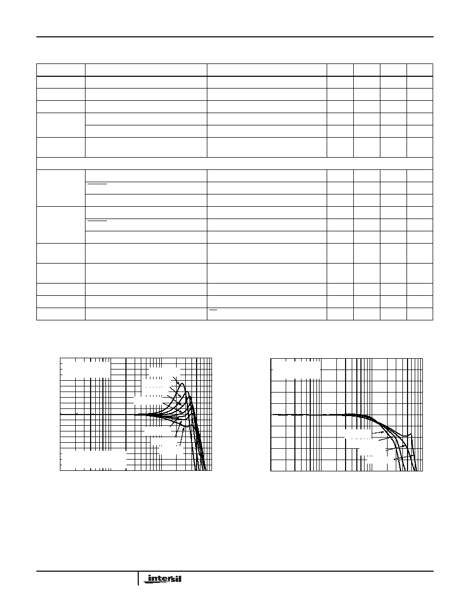
Typical Performance Curves
V
S
=
±
5V, R
L
= 500
to GND, T
A
= 25∞C, unless otherwise specified.
FIGURE 1. GAIN vs FREQUENCY vs C
L
FIGURE 2. GAIN vs FREQUENCY vs R
L
-10
-8
-6
-4
-2
0
2
4
6
8
10
1
10
100
1K
FREQUENCY (MHz)
NORMALIZED GAIN
(
d
B)
C
L
=2.2pF
C
L
=6.2pF
C
L
=16.5pF
C
L
=7.3pF
C
L
=4.7pF
C
L
=1.5pF
SOURCE
POWER=-20dBm
C
L
=11.5pF
C
L
INCLUDES 1.5pF
BOARD CAPACITANCE
-5
-4
-3
-2
-1
0
1
2
3
4
5
1
10
100
1K
FREQUENCY (MHz)
NORMALIZE
D
GAIN
(
d
B
)
R
L
=1k
R
L
=150
R
L
=100
SOURCE
POWER=-20dBm
R
L
=500
EL4340, EL4342

5
FN7421.1
September 21, 2005
FIGURE 3. 0.1dB GAIN vs FREQUENCY
FIGURE 4. R
OUT
vs FREQUENCY
FIGURE 5. EL4340 TRANSIENT RESPONSE
FIGURE 6. EL4342 TRANSIENT RESPONSE
FIGURE 7. EL4340 CROSSTALK
AND OFF ISOLATION
FIGURE 8. EL4342 CROSSTALK
AND OFF ISOLATION
Typical Performance Curves
V
S
=
±
5V, R
L
= 500
to GND, T
A
= 25∞C, unless otherwise specified. (Continued)
10
100
1K
FREQUENCY (MHz)
NORMALIZ
E
D
GA
IN
(dB)
SOURCE
POWER=-20dBm
-0.7
-0.6
-0.4
-0.3
-0.1
0
0.1
-0.2
-0.5
1
≤
C
L
=4.7pF
C
L
=1.5pF
0.2
-0.8
100
10
1
0.1
0.1
1
10
100
1K
FREQUENCY (MHz)
OUTPUT RESIST
ANC
E
(
)
O
U
TP
UT VO
L
T
A
G
E (V)
TIME (5ns/DIV)
0.6
0.4
0.2
0
-0.2
-0.4
-0.6
C
L
=1.5pF
R
L
=500
0.8
-0.8
OUT
P
UT VOL
T
AGE
(V)
TIME (5ns/DIV)
0.6
0.4
0.2
0
-0.2
-0.4
-0.6
C
L
=1.5pF
R
L
=500
-0.8
0.8
FREQUENCY (MHz)
-10
-30
-50
(dB)
0.1
1
10
100
1K
-70
-90
INPUT X TO OUTPUT Y
CROSSTALK
OFF ISOLATION
INPUT X TO OUTPUT X
0
-20
-40
-60
-80
-100
FREQUENCY (MHz)
-10
-30
-50
(dB)
0.1
1
10
100
1K
-70
-90
≤
INPUT X TO OUTPUT Y
CROSSTALK
OFF ISOLATION
INPUT X TO OUTPUT X
0
-20
-40
-60
-80
-100
EL4340, EL4342