 | –≠–ª–µ–∫—Ç—Ä–æ–Ω–Ω—ã–π –∫–æ–º–ø–æ–Ω–µ–Ω—Ç: EL4393 | –°–∫–∞—á–∞—Ç—å:  PDF PDF  ZIP ZIP |

1
Æ
FN7165
CAUTION: These devices are sensitive to electrostatic discharge; follow proper IC Handling Procedures.
1-888-INTERSIL or 321-724-7143
|
Intersil (and design) is a registered trademark of Intersil Americas Inc.
Copyright © Intersil Americas Inc. 2003. All Rights Reserved. Elantec is a registered trademark of Elantec Semiconductor, Inc.
All other trademarks mentioned are the property of their respective owners.
EL4393
Triple 80MHz Video Amplifier w/Disable
The EL4393 is three wideband current-
feedback amplifiers optimized for video
performance. Each amplifier can drive
a load of 150
at video levels. Each amplifier has a disable
capability, which is controlled by a TTL/CMOS compatible
logic signal. The EL4393 operates on supplies as low as ±4V
up to ±15V.
Being a current-feedback design, the bandwidth stays rela-
tively constant at approximately 80MHz over the ±1 to ±10
gain range. The EL4393 has been optimized for use with
1300
feedback resistors at a gain of 2.
When the outputs are disabled, the supply current consump-
tion drops, by about 4mA per channel that is disabled. This
feature can be used to reduce power dissipation.
Pinout
Features
∑ 80MHz -3dB bandwidth for gains of 1 to 10
∑ 900V/µs slew rate
∑ 10MHz bandwidth flat to 0.1dB
∑ Excellent differential gain and phase
∑ TTL/CMOS compatible
∑ Available in SOL-16
Applications
∑ RGB drivers
∑ RGB multiplexers
∑ RGB gain blocks
∑ Video gain blocks
∑ Coax cable driver
∑ ADC drivers/input multiplexer
EL4393
(16-PIN PDIP, SO)
TOP VIEW
Ordering Information
PART
NUMBER
TEMP. RANGE
PACKAGE
PKG. NO.
EL4393CN
-40∞C to +85∞C
16-Pin PDIP
MDP0031
EL4393CM
-40∞C to +85∞C
16-Pin SOL
MDP0027
Data Sheet
January 1996, Rev B
OBSO
LETE
PRO
DUCT
NO R
ECOM
MEN
DED
REPL
ACEM
ENT
conta
ct ou
r Tec
hnica
l Sup
port
Cent
er at
1-888
-INTE
RSIL
or w
ww.in
tersil
.com
/tsc

2
NOTES:
1. V
CM
= ±10V for V
S
= ±15V.
2. V
OS
is measured at V
S
= ±4.5V and V
S
= ±16V, both supplies are changed simultaneously.
3. Only one output short-circuited. Pulse test or use heatsink.
Absolute Maximum Ratings
(T
A
= 25∞C)
Voltage between V
S
+ and V
S
-. . . . . . . . . . . . . . . . . . . . . . . . . .+33V
Voltage at V
S
+ . . . . . . . . . . . . . . . . . . . . . . . . . . . . . . . . . . . . . .+18V
Voltage at V
S
-
. . . . . . . . . . . . . . . . . . . . . . . . . . . . . . . . . . . . . . -18V
Voltage between V
IN
+ and V
IN
-. . . . . . . . . . . . . . . . . . . . . . . . . .±6V
Current into V
IN
+ or V
IN
- . . . . . . . . . . . . . . . . . . . . . . . . . . . . . . 5mA
Internal Power Dissipation . . . . . . . . . . . . . . . . . . . . . . . See Curves
Operating Ambient Temperature Range . . . . . . . . . .-40∞C to +85∞C
Operating Junction Temperature . . . . . . . . . . . . . . . . . . . . . . . 150∞C
Storage Temperature Range . . . . . . . . . . . . . . . . . .-65∞C to +150∞C
CAUTION: Stresses above those listed in "Absolute Maximum Ratings" may cause permanent damage to the device. This is a stress only rating and operation of the
device at these or any other conditions above those indicated in the operational sections of this specification is not implied.
IMPORTANT NOTE: All parameters having Min/Max specifications are guaranteed. Typical values are for information purposes only. Unless otherwise noted, all tests
are at the specified temperature and are pulsed tests, therefore: T
J
= T
C
= T
A
Open-Loop DC Electrical Specifications
Supplies at ±15V, Load = 1k
PARAMETER
DESCRIPTION
TEMP
MIN
TYP
MAX
UNITS
V
OS
Input Offset Voltage
+25∞C
2
±15
mV
TCV
OS
Temperature Coefficient of V
OS
Full
50
µV/∞C
I
B
+
I
IN
+ Input Bias Current
+25∞C
0.2
5
µA
I
B
-
I
IN
- Input Bias Current
+25∞C
10
65
µA
TCI
B
-
Temperature Coefficient of I
B
-
Full
25
nA/∞C
CMRR
Common-Mode Rejection Ratio (Note 1)
+25∞C
50
58
dB
-ICMR
I
IN
- Input Common-Mode Current (Note 1)
+25∞C
3
8
µA/V
PSRR
Power Supply Rejection Ratio (Note 2)
+25∞C
50
58
dB
-IPSR
I
IN
- Current Supply Rejection (Note 2)
+25∞C
2
5
µA/V
R
OL
Transimpedance
+25∞C
100
217
k
R
IN
IN+ Input Impedance
+25∞C
2
M
V
IN
IN+ Input Range
+25∞C
±13
±13.5
V
V
O
Output Voltage Swing; R
L
= 1k
+25∞C
±12
±13
V
I
SC
Short-Circuit Current (Note 3)
+25∞C
40
70
mA
I
O, DIS
Output Current when Disabled
+25∞C
5
150
µA
DIS V
IL
Disable Voltage for Logic Low
+25∞C
0.8
V
DIS V
IH
Disable Voltage for Logic High
+25∞C
2.2
V
DIS I
IL
Disable Logic Low Input Current
+25∞C
3
25
µA
DIS I
IH
Disable Logic High Input Current
+25∞C
0
5
µA
I
CC (en)
Positive Supply Current all Channels Enabled
+25∞C
15
20
±29
mA
I
CC (dis)
Positive Supply Current all Channels Disabled
+25∞C
6
11
16
mA
I
EE (en)
Negative Supply Current all Channels Enabled
+25∞C
13
18
±28
mA
I
EE (dis)
Negative Supply Current all Channels Disabled
+25∞C
4
9
14
mA
EL4393

3
NOTES:
1. Test fixture was designed to minimize capacitance at the I
N
+ input. A "good" fixture should have less than 2pF of stray capacitance to ground at
this very sensitive pin. See application notes for further details.
2. R
L
= 300
, -5V to +5V swing, SR measured at 20% to 80%
3. -2V to +2V swing, SR measured at 20% to 80%.
4. R
L
= 300
.
5. DC offset from -0.7V through +0.7V AC amplitude is 286mV
P-P
, equivalent to 40 ire.
AC Electrical Specifications
Supplies at ±15V, Load = 150
and 15pF, except where noted. Rf1 and Rf2 = 1500
; A
V
= 2,
T
A
= 25∞C.(Note 1)
PARAMETER
DESCRIPTION
MIN
TYP
MAX
UNITS
SR
Slew Rate (Note 2)
960
V/µs
SR
Slew Rate w/±5V Supplies (Note 3)
470
V/µs
t
S
Settling Time to 1% 5V
P-P
5V Step (Note 4)
32
ns
BW
Bandwidth, -3dB
±5V Supplies, -3dB
80
60
MHz
MHz
BW
Bandwidth, -0.1dB
±5V Supplies, -0.1dB
16
21
MHz
MHz
Peaking
-3dB BW Tests
0.6
dB
dG
Differential Gain at 3.58MHz
at ±5V Supplies (Note 5)
0.03
0.30
%
%
d
Differential Phase at 3.58MHz
at ±5V Supplies (Note 5)
0.088
0.096
(∞)
(∞)
EL4393
4
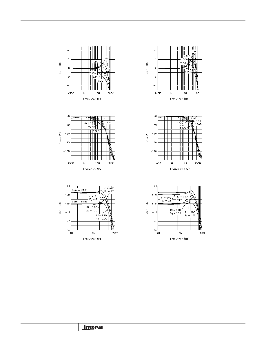
Typical Performance Curves
Gain Flatness vs Rf at ± 5V
Gain Flatness vs Rf at ± 15V
Phase vs Rf at ±15V
Phase vs Rf at ± 5V
Gain of 5, 10 vs Various Rf,
Rg at ±5V
Gain of 5, 10 vs Rf,
Rg at ± 15V
EL4393

5
Typical Performance Curves
(Continued)
Disabled
Isolation Test at ±5V
Disabled
Isolation Test at ± 15V
Voltage Noise
EL4393 MUX Channel
Channel Isolation
Differential Gain & Phase
at 3.58MHz
Cin--vs Peaking
EL4393