 | –≠–ª–µ–∫—Ç—Ä–æ–Ω–Ω—ã–π –∫–æ–º–ø–æ–Ω–µ–Ω—Ç: EL5105IW | –°–∫–∞—á–∞—Ç—å:  PDF PDF  ZIP ZIP |

1
Æ
FN7332
CAUTION: These devices are sensitive to electrostatic discharge; follow proper IC Handling Procedures.
1-888-INTERSIL or 321-724-7143
|
Intersil (and design) is a registered trademark of Intersil Americas Inc.
Copyright © Intersil Americas Inc. 2004. All Rights Reserved. Elantec is a registered trademark of Elantec Semiconductor, Inc.
All other trademarks mentioned are the property of their respective owners.
P R E L I M I N A R Y
EL5104, EL5105, EL5204, EL5205, EL5304
700MHz Slew Enhanced VFA
The EL5104, EL5105, EL5204,
EL5205, and EL5304 represent high-
speed voltage feedback amplifiers
based on the current feedback amplifier architecture. This
gives the typical high slew rate benefits of a CFA family
along with the stability and ease of use associated with the
VFA type architecture. This family is available in single, dual,
and triple versions, with 200MHz, 400MHz, and 700MHz
versions. These are all available in single, dual and triple
versions. This family operates on single 5V or ±5V supplies
from minimum supply current. The EL5104 and EL5204 also
feature an output enable function, which can be used to put
the output in to a high-impedance mode. This enables the
outputs of multiple amplifiers to be tied together for use in
multiplexing applications.
Features
∑ Specified for 5V or ±5V applications
∑ Power-down to 17µA
∑ -3dB bandwidth = 700MHz
∑ ±0.1dB bandwidth = 45MHz
∑ Low supply current = 9.5mA
∑ Slew rate = 3000V/µs
∑ Low offset voltage = 10mV max
∑ Output current = 160mA
∑ A
VOL
= 1400
∑ Diff gain/phase = 0.01%/0.02∞C
Applications
∑ Video amplifiers
∑ PCMCIA applications
∑ A/D drivers
∑ Line drivers
∑ Portable computers
∑ High speed communications
∑ RGB applications
∑ Broadcast equipment
∑ Active filtering
Ordering Information
PART
NUMBER
PACKAGE
TAPE & REEL
PKG. DWG. #
EL5104IS
8-Pin SO
-
MDP0027
EL5104IS-T7
8-Pin SO
7"
MDP0027
EL5104IS-T13
8-Pin SO
13"
MDP0027
EL5104IW-T7
6-Pin SOT-23
7" (3K pcs)
MDP0038
EL5104IW-T7A
6-Pin SOT-23
7" (250 pcs)
MDP0038
EL5105IC-T7
5-Pin SC-70
7" (3K pcs)
P5.049
EL5105IC-T7A
5-Pin SC-70
7" (250 pcs)
P5.049
EL5105IW-T7
5-Pin SOT-23
7" (3K pcs)
MDP0038
EL5105IW-T7A
5-Pin SOT-23
7" (250 pcs)
MDP0038
EL5204IY
10-Pin MSOP
-
MDP0043
EL5204IY-T7
10-Pin MSOP
7"
MDP0043
EL5204IY-T13
10-Pin MSOP
13"
MDP0043
EL5205IS
8-Pin SO
-
MDP0027
EL5205IS-T7
8-Pin SO
7"
MDP0027
EL5205IS-T13
8-Pin SO
13"
MDP0027
EL5205IY
8-Pin MSOP
-
MDP0043
EL5205IY-T7
8-Pin MSOP
7"
MDP0043
EL5205IY-T13
8-Pin MSOP
13"
MDP0043
EL5304IU
16-Pin QSOP
-
MDP0040
EL5304IU-T7
16-Pin QSOP
7"
MDP0040
EL5304IU-T13
16-Pin QSOP
13"
MDP0040
Data Sheet
May 3, 2004
2
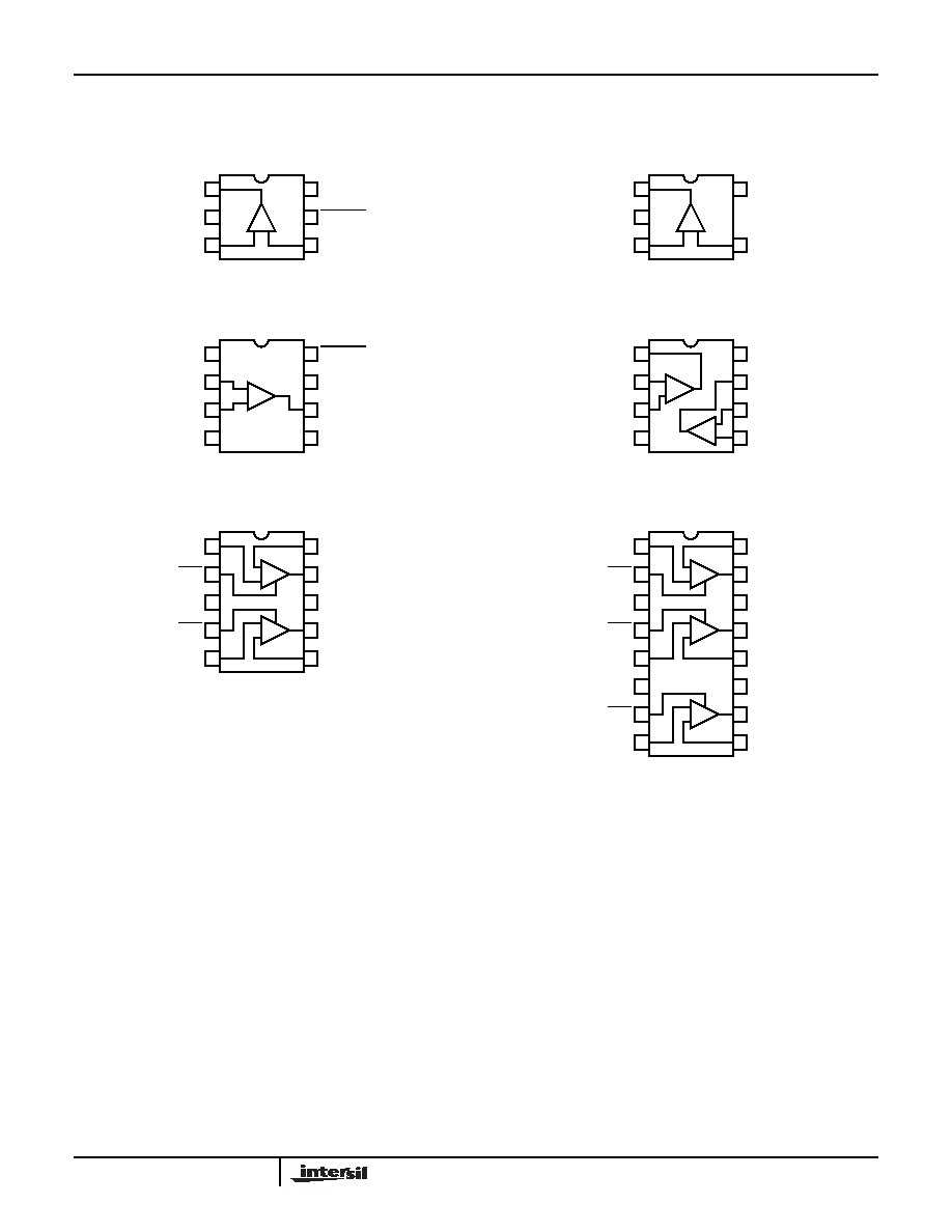
Pinouts
EL5104
(6-PIN SOT-23)
TOP VIEW
EL5105
(5-PIN SOT-23, SC-70)
TOP VIEW
EL5104
(8-PIN SO)
TOP VIEW
EL5205
(8-PIN SO, MSOP)
TOP VIEW
EL5204
(10-PIN MSOP)
TOP VIEW
EL5304
(16-PIN QSOP)
TOP VIEW
1
2
3
6
4
5
+ -
OUT
VS-
IN+
VS+
ENABLE
IN-
1
2
3
5
4
+ -
OUT
VS-
IN+
VS+
IN-
1
2
3
4
8
7
6
5
-
+
NC
IN-
IN+
VS-
ENABLE
VS+
OUT
NC
1
2
3
4
8
7
6
5
-
+
-
+
OUTA
INA-
INA+
VS-
VS+
OUTB
INB-
INB+
1
2
3
4
10
9
8
7
5
6
-
+
-
+
INA+
CEA
VS-
CEB
INA-
OUTA
VS+
OUTB
INB+
INB-
1
2
3
4
16
15
14
13
5
6
7
12
11
10
8
9
-
+
-
+
-
+
INA+
CEA
VS-
CEB
INA-
OUTA
VS+
OUTB
INB+
NC
CEC
INC+
INB-
NC
OUTC
INC-
EL5104, EL5105, EL5204, EL5205, EL5304
3
Absolute Maximum Ratings
(T
A
= 25
∞
C)
Supply Voltage between V
S
+ and GND. . . . . . . . . . . . . . . . . . 13.2V
Input Voltage . . . . . . . . . . . . . . . . . . . . . . . . . . . . . . . . . . . . . . . ±V
S
Differential Input Voltage . . . . . . . . . . . . . . . . . . . . . . . . . . . . . . .±4V
Maximum Output Current. . . . . . . . . . . . . . . . . . . . . . . . . . . . . 80mA
Storage Temperature Range . . . . . . . . . . . . . . . . . . -65∞C to +150∞C
Ambient Operating Temperature Range . . . . . . . . . . -40∞C to +85∞C
Operating Junction Temperature . . . . . . . . . . . . . . . . . . . . . . . 150∞C
CAUTION: Stresses above those listed in "Absolute Maximum Ratings" may cause permanent damage to the device. This is a stress only rating and operation of the
device at these or any other conditions above those indicated in the operational sections of this specification is not implied.
IMPORTANT NOTE: All parameters having Min/Max specifications are guaranteed. Typical values are for information purposes only. Unless otherwise noted, all tests
are at the specified temperature and are pulsed tests, therefore: T
J
= T
C
= T
A
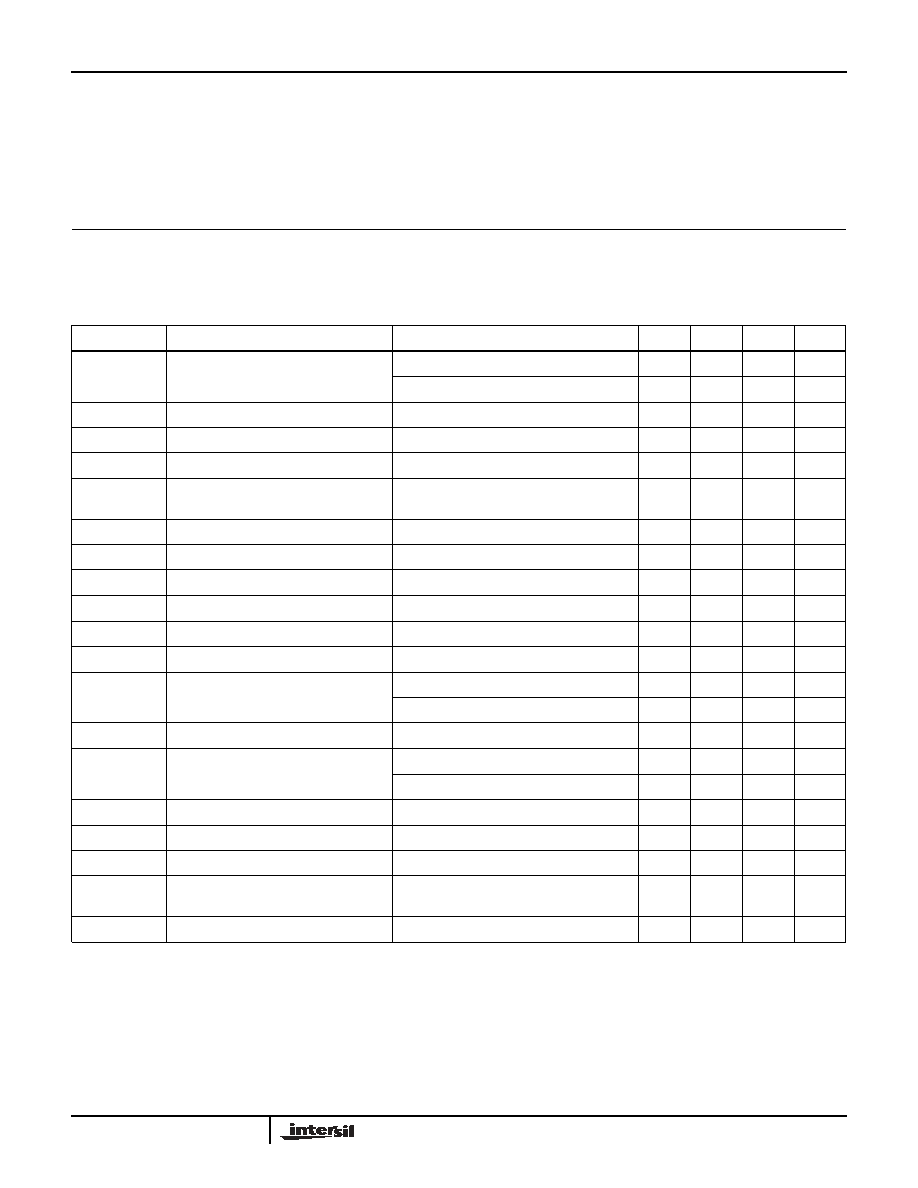
DC Electrical Specifications
V
S
= ±5V, GND = 0V, T
A
= 25∞C, V
CM
= 0V, V
OUT
= 0V, V
ENABLE
= GND or OPEN, unless otherwise
specified.
PARAMETER
DESCRIPTION
CONDITIONS
MIN
TYP
MAX
UNIT
V
OS
Offset Voltage
EL5104, EL5105, EL5204, EL5205
-10
3
10
mV
EL5304
-18
5
18
mV
TCV
OS
Offset Voltage Temperature Coefficient
Measured from T
MIN
to T
MAX
10
µV/∞C
IB
Input Bias Current
V
IN
= 0V
8
30
µA
I
OS
Input Offset Current
V
IN
= 0V
4
15
µA
TCI
OS
Input Bias Current Temperature
Coefficient
Measured from T
MIN
to T
MAX
50
nA/∞C
PSRR
Power Supply Rejection Ratio
60
70
dB
CMRR
Common Mode Rejection Ratio
V
CM
from -3V to +3V
56
62
dB
CMIR
Common Mode Input Range
Guaranteed by CMRR test
-3
+3
V
R
IN
Input Resistance
Common mode
50
120
K
C
IN
Input Capacitance
SO package
1
pF
I
S,ON
Supply Current - Enabled
8.5
9.5
11
mA
I
S,OFF
Supply Current - Shut Down
V
S
+
0
10
µA
V
S
-
17
70
µA
PSOR
Power Supply Operating Range
4
13.2
V
AVOL
Open Loop Gain
R
L
= 1k
to GND
55
65
dB
R
L
= 150
to GND
60
dB
V
OP
Positive Output Voltage Swing
R
L
= 150
to 0V
3.6
3.8
V
V
ON
Negative Output Voltage Swing
R
L
= 150
to 0V
-3.8
-3.6
V
I
OUT
Output Current
R
L
= 10
to 0V
±90
±160
mA
V
IH-EN
ENABLE pin Voltage for Power Up
(V
S
+)
-2.5
(V
S
+)
-1.0
V
V
IL-EN
ENABLE pin Voltage for Shut Down
0.5
V
EL5104, EL5105, EL5204, EL5205, EL5304
4
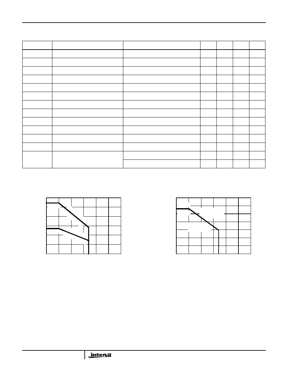
Closed Loop AC Electrical Specifications
V
S
= +5V, GND = 0V, T
A
= 25∞C, V
CM
= +1.5V, V
OUT
= +1.5V,
V
CLAMP
= +5V,
V
ENABLE
= +5V, A
V
= +1, R
F
= 0
, R
L
= 150
to GND pin, unless otherwise specified.
PARAMETER
DESCRIPTION
CONDITIONS
MIN
TYP
MAX
UNIT
BW
-3dB Bandwidth (V
OUT
= 200mV
P-P
)
V
S
= ±5V, A
V
= 1, R
F
= 0
700
MHz
SR
Slew Rate
R
L
= 150
, V
OUT
= -2.5V to +2.5V
2000
3000
5000
V/µs
t
R
,t
F
Rise Time, Fall Time
±0.1V step
0.4
ns
OS
Overshoot
±0.1V step
10
%
t
PD
Propagation Delay
±0.1V step
0.4
ns
t
S
0.1% Settling Time
V
S
= ±5V, R
L
= 500
, A
V
= 1, V
OUT
= ±2.5V
7
ns
dG
Differential Gain
A
V
= 2, R
L
= 150
, V
INDC
= -1 to +1V
0.01
%
dP
Differential Phase
A
V
= 2, R
L
= 150
, V
INDC
= -1 to +1V
0.02
∞
e
N
Input Noise Voltage
f = 10kHz
10
nV/
Hz
i
N
Input Noise Current
f = 10kHz
54
pA/
Hz
t
DIS
Disable Time
180
ns
t
EN
Enable Time
650
ns
I
EN
Enable Pin Current
Enabled, V
EN
= 0V
-1
1
µA
Disabled, V
EN
= 5V
5
25
µA
Typical Performance Curves
FIGURE 1. PACKAGE POWER DISSIPATION vs AMBIENT
TEMPERATURE
FIGURE 2. PACKAGE POWER DISSIPATION vs AMBIENT
TEMPERATURE
JEDEC JESD51-7 HIGH EFFECTIVE THERMAL
CONDUCTIVITY TEST BOARD
1.2
1
0.4
0
0
25
50
75
100
150
AMBIENT TEMPERATURE (∞C)
POWE
R DI
SSI
PATI
ON (
W
)
85
1.087W
0.8
0.2
0.6
543mW
125
JA
=11
5∞C
/W
MS
OP
8/1
0
JA
=230∞
C/W
SOT2
3-5/6
1.116W
JA
=112∞C/W
QSOP16
1.136W
JA
=110∞C/W
SO8
1.4
0.8
0.6
0.2
0
0
25
50
75
100
150
AMBIENT TEMPERATURE (∞C)
POWE
R DI
SSI
PATI
ON (
W
)
125
85
JEDEC JESD51-7 HIGH EFFECTIVE THERMAL
CONDUCTIVITY TEST BOARD
0.4
1
1.2
EL5104, EL5105, EL5204, EL5205, EL5304
5
All Intersil U.S. products are manufactured, assembled and tested utilizing ISO9000 quality systems.
Intersil Corporation's quality certifications can be viewed at www.intersil.com/design/quality
Intersil products are sold by description only. Intersil Corporation reserves the right to make changes in circuit design, software and/or specifications at any time without
notice. Accordingly, the reader is cautioned to verify that data sheets are current before placing orders. Information furnished by Intersil is believed to be accurate and
reliable. However, no responsibility is assumed by Intersil or its subsidiaries for its use; nor for any infringements of patents or other rights of third parties which may result
from its use. No license is granted by implication or otherwise under any patent or patent rights of Intersil or its subsidiaries.
For information regarding Intersil Corporation and its products, see www.intersil.com
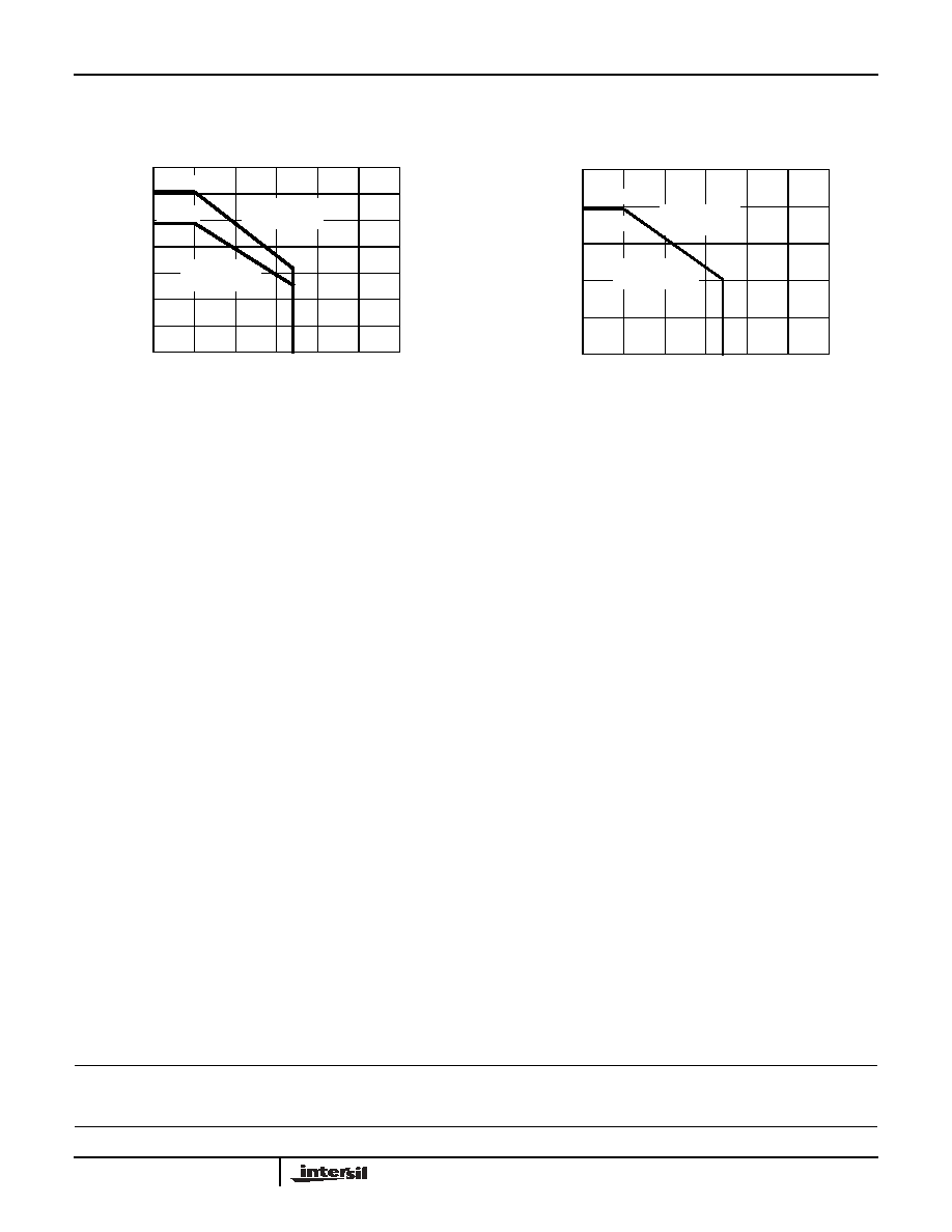
FIGURE 3. PACKAGE POWER DISSIPATION vs AMBIENT
TEMPERATURE
FIGURE 4. PACKAGE POWER DISSIPATION vs AMBIENT
TEMPERATURE
Typical Performance Curves
JEDEC JESD51-3 LOW EFFECTIVE THERMAL
CONDUCTIVITY TEST BOARD
0.7
0.6
0.4
0.3
0.2
0.1
0
0
25
50
75
100
150
AMBIENT TEMPERATURE (∞C)
POWE
R DI
SSI
PATI
ON (
W
)
85
607mW
JA
=206∞C/W
MSOP8/10
0.5
488mW
JA
=256∞C/W
SOT23-5/6
125
791mW
JA
=158∞C/W
QSOP16
781mW
JA
=160∞C/W
SO8
1
0.8
0.6
0.2
0
0
25
50
75
100
150
AMBIENT TEMPERATURE (∞C)
POWER DISS
IP
AT
ION (W)
125
85
JEDEC JESD51-3 LOW EFFECTIVE THERMAL
CONDUCTIVITY TEST BOARD
0.4
EL5104, EL5105, EL5204, EL5205, EL5304