1
HA-2520, HA-2522,
HA-2525
20MHz, High Slew Rate, Uncompensated,
High Input Impedance, Operational
Amplifiers
HA-2520/2522/2525 comprise a series of operational amplifiers
delivering an unsurpassed combination of specifications for
slew rate, bandwidth and settling time. These dielectrically
isolated amplifiers are controlled at close loop gains greater
than 3 without external compensation. In addition, these high
performance components also provide low offset current and
high input impedance.
120V/
µ
s slew rate and 200ns (0.2%) settling time of these
amplifiers make them ideal components for pulse amplification
and data acquisition designs. These devices are valuable
components for RF and video circuitry requiring up to 20MHz
gain bandwidth and 2MHz power bandwidth. For accurate signal
conditioning designs the HA-2520/2522/2525's superior dynamic
specifications are complemented by 10nA offset current, 100M
input impedance and offset trim capability. MIL-STD-883 product
and data sheets are available upon request.
Features
∑ High Slew Rate. . . . . . . . . . . . . . . . . . . . . . . . . . . 120V/
µ
s
∑ Fast Settling . . . . . . . . . . . . . . . . . . . . . . . . . . . . . . . 200ns
∑ Full Power Bandwidth . . . . . . . . . . . . . . . . . . . . . . . . 2MHz
∑ Gain Bandwidth (A
V
3) . . . . . . . . . . . . . . . . . . . . 20MHz
∑ High Input Impedance . . . . . . . . . . . . . . . . . . . . . . 100M
∑ Low Offset Current . . . . . . . . . . . . . . . . . . . . . . . . . . .10nA
∑ Compensation Pin for Unity Gain Capability
Applications
∑ Data Acquisition Systems
∑ RF Amplifiers
∑ Video Amplifiers
∑ Signal Generators
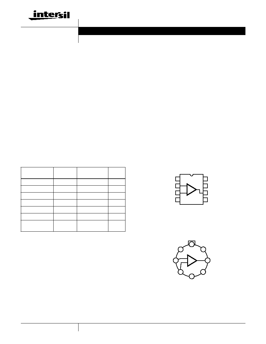
Pinouts
HA-2520 (CERDIP)
HA-2525 (PDIP, CERDIP, SOIC)
TOP VIEW
HA-2520/22/25
(METAL CAN)
TOP VIEW
Ordering Information
PART NUMBER
(BRAND)
TEMP.
RANGE (
o
C)
PACKAGE
PKG.
NO.
HA2-2520-2
-55 to 125
8 Pin Metal Can
T8.C
HA2-2522-2
-55 to 125
8 Pin Metal Can
T8.C
HA2-2525-5
0 to 75
8 Pin Metal Can
T8.C
HA3-2525-5
0 to 75
8 Ld PDIP
E8.3
HA7-2520-2
-55 to 125
8 Ld CERDIP
F8.3A
HA7-2525-5
0 to 75
8 Ld CERDIP
F8.3A
HA9P2525-5
(H25255)
0 to 75
8 Ld SOIC
M8.15
BAL
-IN
+IN
V-
1
2
3
4
8
7
6
5
COMP
V+
OUT
BAL
-
+
COMP
OUT
IN-
V-
BAL
IN+
V+
BAL
2
4
6
1
3
7
5
8
-
+
Data Sheet
September 1998
File Number
2894.3
CAUTION: These devices are sensitive to electrostatic discharge; follow proper IC Handling Procedures.
1-888-INTERSIL or 321-724-7143
|
Copyright
©
Intersil Corporation 1999

2
Absolute Maximum Ratings
Thermal Information
Supply Voltage (Between V+ and V- Terminals) . . . . . . . . . . . . 40V
Differential Input Voltage . . . . . . . . . . . . . . . . . . . . . . . . . . . . . . 15V
Output Current . . . . . . . . . . . . . . . . . . . . . . . . . . . . . . . . . . . . . 50mA
Operating Conditions
Temperature Range
HA-2520/2522-2 . . . . . . . . . . . . . . . . . . . . . . . . . . -55
o
C to 125
o
C
HA-2525-5 . . . . . . . . . . . . . . . . . . . . . . . . . . . . . . . . 0
o
C to 75
o
C
Thermal Resistance (Typical, Note 1)
JA
(
o
C/W)
JC
(
o
C/W)
Metal Can Package . . . . . . . . . . . . . . .
165
80
PDIP Package . . . . . . . . . . . . . . . . . . .
96
N/A
CERDIP Package . . . . . . . . . . . . . . . . .
135
50
SOIC Package . . . . . . . . . . . . . . . . . . .
157
N/A
Maximum Junction Temperature (Hermetic Packages). . . . . . . 175
o
C
Maximum Junction Temperature (Plastic Package) . . . . . . . 150
o
C
Maximum Storage Temperature Range . . . . . . . . . . -65
o
C to 150
o
C
Maximum Lead Temperature (Soldering 10s) . . . . . . . . . . . . 300
o
C
(SOIC - Lead Tips Only)
CAUTION: Stresses above those listed in "Absolute Maximum Ratings" may cause permanent damage to the device. This is a stress only rating and operation of the
device at these or any other conditions above those indicated in the operational sections of this specification is not implied.
NOTE:
1.
JA
is measured with the component mounted on an evaluation PC board in free air.
Electrical Specifications
V
SUPPLY
=
±
15V
PARAMETER
TEMP
(
o
C)
HA-2520-2
HA-2522-2
HA-2525-5
UNITS
MIN
TYP
MAX
MIN
TYP
MAX
MIN
TYP
MAX
INPUT CHARACTERISTICS
Offset Voltage
25
-
4
8
-
5
10
-
5
10
mV
Full
-
-
11
-
-
14
-
-
14
mV
Offset Voltage Drift
Full
-
20
-
-
25
-
-
30
-
µ
V/
o
C
Bias Current
25
-
100
200
-
125
250
-
125
250
nA
Full
-
-
400
-
-
500
-
-
500
nA
Offset Current
25
-
10
25
-
20
50
-
20
50
nA
Full
-
-
50
-
-
100
-
-
100
nA
Input Resistance (Note 2)
25
50
100
-
40
100
-
40
100
-
M
Common Mode Range
Full
±
10.0
-
-
±
10.0
-
-
±
10.0
-
-
V
TRANSFER CHARACTERISTICS
Large Signal Voltage Gain
(Notes 3, 6)
25
10
15
-
7.5
15
-
7.5
15
-
kV/V
Full
7.5
-
-
5
-
--
5
-
-
kV/V
Common Mode Rejection Ratio
(Note 4)
Full
80
90
-
74
90
-
74
90
-
dB
Gain Bandwidth (Notes 2, 5)
25
10
20
-
10
20
-
10
20
-
MHz
Minimum Stable Gain
25
3
-
-
3
-
-
3
-
-
V/V
OUTPUT CHARACTERISTICS
Output Voltage Swing (Note 3)
Full
±
10.0
±
12.0
-
±
10.0
±
12.0
-
±
10.0
±
12.0
-
V
Output Current (Note 6)
25
±
10
±
20
-
±
10
±
20
-
±
10
±
20
-
mA
Full Power Bandwidth
(Notes 6, 11)
25
1.5
2.0
-
1.2
2.0
-
1.2
2.0
-
MHz
TRANSIENT RESPONSE (A
V
= +3)
Rise Time (Notes 3, 7, 8, 10)
25
-
25
50
-
25
50
-
25
50
ns
Overshoot (Notes 3, 7, 8, 10)
25
-
25
40
-
25
50
-
25
50
%
Slew Rate (Notes 3, 7, 10, 12)
25
±
100
±
120
-
±
80
±
120
-
±
80
±
120
-
V/
µ
s
Settling Time (Notes 3, 7, 10, 12)
25
-
0.20
-
-
0.20
-
-
0.20
-
µ
s
HA-2520, HA-2522, HA-2525

3
POWER SUPPLY CHARACTERISTICS
Supply Current
25
-
4
6
-
4
6
-
4
6
mA
Power Supply Rejection Ratio (Note 9)
Full
80
90
-
74
90
-
74
90
-
dB
NOTES:
2. This parameter value is based on design calculations.
3. R
L
= 2k
.
4. V
CM
=
±
10V.
5. A
V
> 10.
6. V
O
=
±
10.0V.
7. C
L
= 50pF.
8. V
O
=
±
200mV.
9.
V =
±
5.0V.
10. See Transient Response Test Circuits and Waveforms.
11. Full Power Bandwidth guaranteed based on slew rate measurement using:
.
12. V
OUT
=
±
5V.
Electrical Specifications
V
SUPPLY
=
±
15V (Continued)
PARAMETER
TEMP
(
o
C)
HA-2520-2
HA-2522-2
HA-2525-5
UNITS
MIN
TYP
MAX
MIN
TYP
MAX
MIN
TYP
MAX
FPBW
Slew Rate
2
V
PEAK
-----------------------------
=
Test Circuits and Waveforms
FIGURE 1. SLEW RATE AND SETTLING TIME
NOTE: Measured on both positive and negative transitions from 0V
to +200mV and 0V to -200mV at the output.
FIGURE 2. TRANSIENT RESPONSE
FIGURE 3. SLEW RATE AND TRANSIENT RESPONSE
NOTES:
13. A
V
= -3.
14. Feedback and summing resistor ratios should be 0.1% matched.
15. Clipping diodes CR
1
and CR
2
are optional. HP5082-2810
recommended.
FIGURE 4. SETTLING TIME TEST CIRCUIT
+1.67V
INPUT
+5V
75%
OUTPUT
25%
ERROR BAND
±
10mV FROM
FINAL VALUE
t
SLEW
=
V/
t
-1.67V
SETTLING
TIME
V
-5V
RATE
INPUT
90%
OUTPUT
10%
0V
RISE TIME
±
67mV
0V
±
200mV
OVERSHOOT
OUT
IN
+
1333
50pF
-
667
5pF
OUTPUT
INPUT
667.2
1667
2
3
4
6
7
100pF
V+
V-
D
G
S
2N4416
CR
1
CR
2
SETTLING TIME
TEST POINT
1
µ
F
0.001
µ
F
1
µ
F
0.001
µ
F
2001
4999.9
2000
+
-
HA-2520, HA-2522, HA-2525

4
All Intersil semiconductor products are manufactured, assembled and tested under ISO9000 quality systems certification.
Intersil semiconductor products are sold by description only. Intersil Corporation reserves the right to make changes in circuit design and/or specifications at any time with-
out notice. Accordingly, the reader is cautioned to verify that data sheets are current before placing orders. Information furnished by Intersil is believed to be accurate and
reliable. However, no responsibility is assumed by Intersil or its subsidiaries for its use; nor for any infringements of patents or other rights of third parties which may result
from its use. No license is granted by implication or otherwise under any patent or patent rights of Intersil or its subsidiaries.
For information regarding Intersil Corporation and its products, see web site http://www.intersil.com
Schematic Diagram
NOTE: Tested offset adjustment range is |V
OS
+ 1mV| minimum referred to output. Typical ranges are
±
20mV with R
T
= 20k
.
FIGURE 5. SUGGESTED V
OS
ADJUSTMENT AND COMPENSATION HOOK-UP
Test Circuits and Waveforms
(Continued)
OUT
IN
BAL.
V-
V+
20k
COMP
C
C
Q
29
Q
30
R
11
R
10
200
R
2BB
R
21
200
R
2AA
440
1.8K
R
2B
Q
3B
Q
3A
1.8K
R
2A
Q
4B
Q
4A
Q
18
Q
19
Q
20
Q
21A
Q
25
Q
22
R
6A
R
6B
Q
1B
Q
1A
Q
2A
Q
2B
R
1A
R
1B
Q
17
R
16
R
15
R
13
Q
28
Q
27
Q
24
Q
31
Q
26
Q
21B
Q
5A
Q
5B
R
3A
R
3B
R
19
Q
10
R
10
D
14
Q
16
Q
8
Q
23
V+
R
12
Q
15
Q
12A
R
9
D
138
Q
12B
Q
11B
OUTPUT
Q
7
Q
6
D
13A
Q
11A
Q
9
V-
+INPUT
BAL 1
BAL 2
OFFSET
-
OFFSET+
-INPUT
PIN 1
440
C
1
1pF
COMP
R
18
30
R
17
50
HA-2520, HA-2522, HA-2525
5
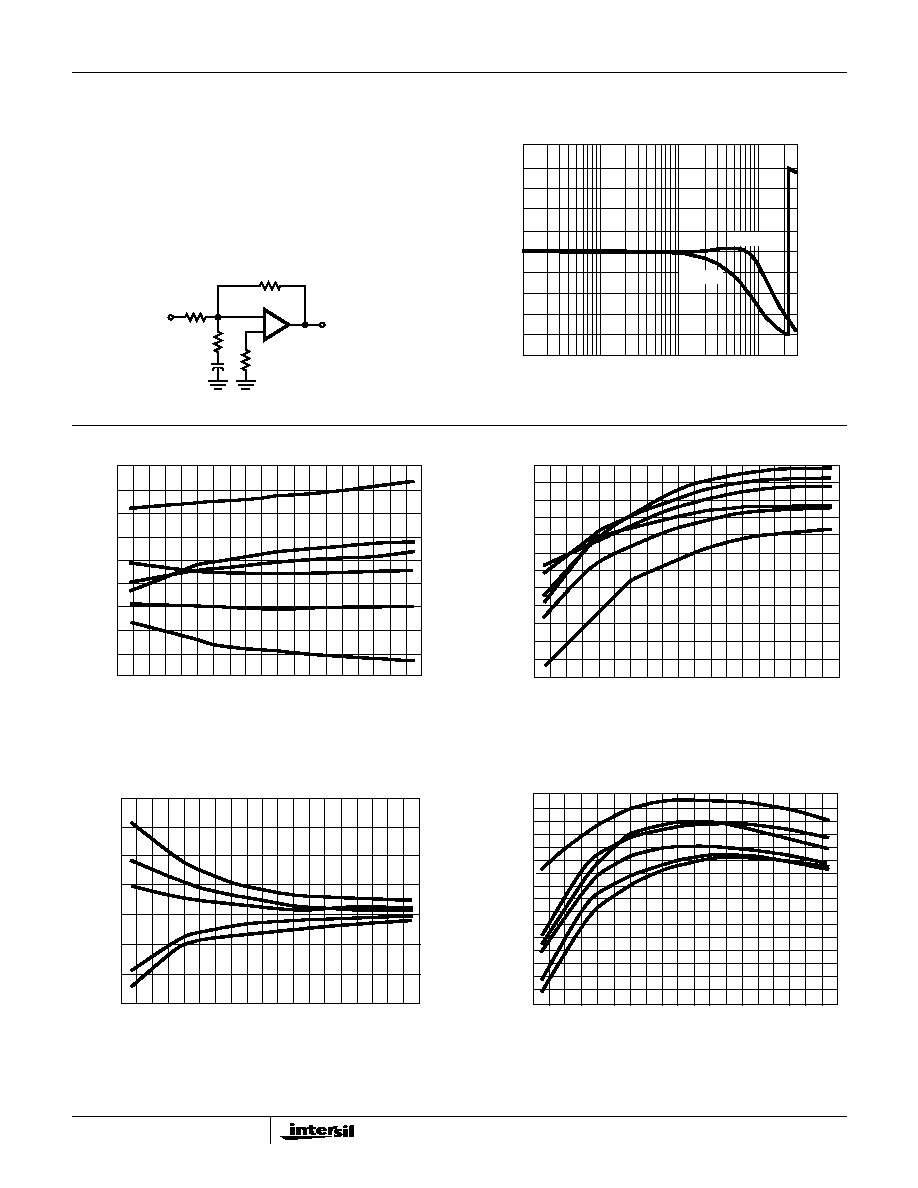
Typical Application
Inverting Unity Gain Circuit
Figure 6 shows a Compensation Circuit for an inverting unity
gain amplifier. The circuit was tested for functionality with
supply voltages from
±
4V to
±
15V, and the performance as
tested was: Slew Rate
120V/
µ
s; Bandwidth
10MHz; and
Settling Time (0.1%)
500ns. Figure 7 illustrates the amplifier's
frequency response, and it is important to note that capacitance
at pin 8 must be minimized for maximum bandwidth.
10K
OUT
HA-2520
5K
500pF
2K
10K
IN
+
-
FIGURE 6. INVERTING UNITY GAIN CIRCUIT
GAIN (dB)
GAIN
PHASE
PHASE SHIFT (DEGREES)
15
10
5
0
-5
-10
-15
10K
100K
1M
10M
0
-45
-90
-135
-180
FIGURE 7. FREQUENCY RESPONSE FOR INVERTING UNITY
GAIN CIRCUIT
Typical Performance Curves
V
S
=
±
15V, T
A
= 25
o
C, Unless Otherwise Specified
FIGURE 8. OFFSET VOLTAGE vs TEMPERATURE (6 TYPICAL
UNITS FROM 3 LOTS)
FIGURE 9. BIAS CURRENT vs TEMPERATURE (6 TYPICAL
UNITS FROM 3 LOTS)
FIGURE 10. OFFSET CURRENT vs TEMPERATURE (5 TYPICAL
UNITS FROM 3 LOTS)
FIGURE 11. OPEN LOOP GAIN vs TEMPERATURE (6 TYPICAL
UNITS FROM 3 LOTS)
TEMPERATURE (
o
C)
0
20
40
60
80
100
120
-20
-40
OFFSET V
O
L
T
A
GE (mV)
0
1
2
3
4
5
6
-3
-2
-1
-60
TEMPERATURE (
o
C)
0
20
40
60
80
100
120
-20
-40
-60
-160
-150
-140
-130
-120
-110
-100
-90
-80
-70
-60
-50
-40
BIAS CURRENT (nA)
TEMPERATURE (
o
C)
0
20
40
60
80
100
120
-20
-40
-60
40
30
20
10
0
-30
-20
-10
OFFSET BIAS CURRENT (nA)
TEMPERATURE (
o
C)
0
20
40
60
80
100
120
-20
-40
-60
22
21
20
19
18
17
16
15
14
13
12
11
10
9
8
6
7
A
VO
L
(kV/ V)
HA-2520, HA-2522, HA-2525