1
Æ
CAUTION: These devices are sensitive to electrostatic discharge; follow proper IC Handling Procedures.
1-888-INTERSIL or 321-724-7143
|
Intersil (and design) is a registered trademark of Intersil Americas Inc.
Copyright © Intersil Americas Inc. 2002. All Rights Reserved
HA-2529
20MHz, High Input Impedance,
High Slew Rate Operational Amplifier
The HA-2529 is a monolithic operational amplifier which
typifies excellence of design. With a design based on years of
experience coupled with the reliable dielectric isolation
process, this amplifier provides an outstanding combination of
DC and AC parameters at closed loop gains greater than 3.
The HA-2529 offers 150V/
µ
s slew rate and fast settling time
(200ns), while consuming a mere 6mA of quiescent current,
making this amplifier ideal for video circuitry and data
acquisition designs. With 20MHz gain bandwidth combined
with 7.5kV/V open loop gain, the HA-2529 is an ideal
component for demanding signal conditioning designs. This
device provides
±
30mA output current drive with an output
voltage swing of
±
10V making it suited for pulse amplifier
and RF amplifier components.
The HA-2529 will upgrade output current, slew rate, offset
voltage drift and offset current drift in systems presently
using the HA-2520/22/25 or EHA-2520/22/25.
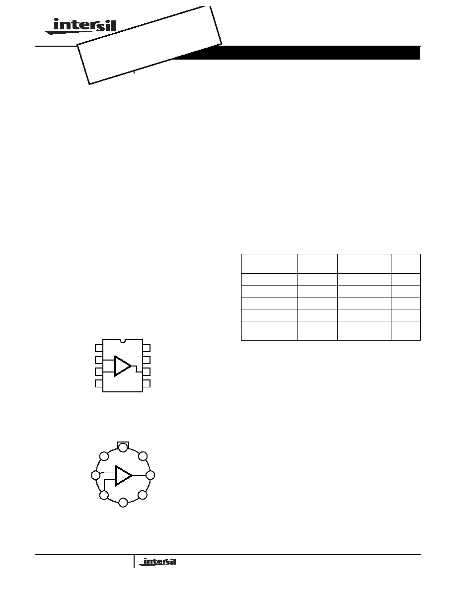
Pinout
MIL-STD-883 product and data sheets are available upon
request.
HA-2529
(PDIP, CERDIP, SOIC)
TOP VIEW
HA-2529
(METAL CAN)
TOP VIEW
Features
∑ High Slew Rate . . . . . . . . . . . . . . . . . . . . . . . . . . 150V/
µ
s
∑ Fast Settling . . . . . . . . . . . . . . . . . . . . . . . . . . . . . . 200ns
∑ Full Power Bandwidth . . . . . . . . . . . . . . . . . . . . . . . 2MHz
∑ Gain Bandwidth (A
V
3) . . . . . . . . . . . . . . . . . . . . 20MHz
∑ High Input Impedance . . . . . . . . . . . . . . . . . . . . . . 130M
∑ Low Offset Current . . . . . . . . . . . . . . . . . . . . . . . . . . . 5nA
∑ High Output Current . . . . . . . . . . . . . . . . . . . . . . . .
±
30mA
Applications
∑ Data Acquisition Systems
∑ Signal Generators
∑ RF Amplifiers
∑ Pulse Amplification
∑ Video Amplifiers
BAL
-IN
+IN
V-
1
2
3
4
8
7
6
5
COMP
V+
OUT
BAL
-
+
COMP
OUT
-IN
V-
BAL
+IN
V+
BAL
2
4
6
1
3
7
5
8
-
+
Part Number Information
PART NUMBER
(BRAND)
TEMP.
RANGE (
o
C)
PACKAGE
PKG.
NO.
HA2-2529-2
-55 to 125
8 Pin Metal Can
T8.C
HA2-2529-5
0 to 75
8 Pin Metal Can
T8.C
HA3-2529-5
0 to 75
8 Ld PDIP
E8.3
HA7-2529-5
0 to 75
8 Ld CERDIP
F8.3A
HA9P2529-5
(H25295)
0 to 75
8 Ld SOIC
M8.15
September 1998
File Number 2895.3
OBSO
LETE
PRO
DUCT
See H
A-252
0, HA
-2522
, HA-
2525
conta
ct ou
r Tec
hnica
l Sup
port C
enter
at
1-888
-INTE
RSIL
or ww
w.int
ersil.
com/
tsc

2
Absolute Maximum Ratings
Thermal Information
Voltage Between V+ and V- Terminals . . . . . . . . . . . . . . . . . . . 40V
Differential Input Voltage . . . . . . . . . . . . . . . . . . . . . . . . . . . . . . 15V
Peak Output Current . . . . . . . . . . . . . . . . . . . . . . . . . . . . . . . . 90mA
Operating Conditions
Temperature Range
HA-2529-2 . . . . . . . . . . . . . . . . . . . . . . . . . . . . . . -55
o
C to 125
o
C
HA-2529-5 . . . . . . . . . . . . . . . . . . . . . . . . . . . . . . . . 0
o
C to 75
o
C
Thermal Resistance (Typical, Note 1)
JA
(
o
C/W)
JC
(
o
C/W)
Metal Can Package . . . . . . . . . . . . . . .
165
80
PDIP Package . . . . . . . . . . . . . . . . . . .
96
N/A
CERDIP Package. . . . . . . . . . . . . . . . .
135
50
SOIC Package . . . . . . . . . . . . . . . . . . .
157
N/A
Maximum Junction Temperature (Hermetic Package) . . . . . . . . 175
o
C
Maximum Junction Temperature (Plastic Package) . . . . . . . .150
o
C
Maximum Storage Temperature Range . . . . . . . . .-65
o
C to 150
o
C
Maximum Lead Temperature (Soldering 10s) . . . . . . . . . . . . 300
o
C
(SOIC - Lead Tips Only)
CAUTION: Stresses above those listed in "Absolute Maximum Ratings" may cause permanent damage to the device. This is a stress only rating and operation of the
device at these or any other conditions above those indicated in the operational sections of this specification is not implied.
NOTE:
1.
JA
is measured with the component mounted on an evaluation PC board in free air.
Electrical Specifications
V
SUPPLY
=
±
15V, C
L
= 50pF, R
L
= 2k
, Unless Otherwise Specified
PARAMETER
TEST CONDITIONS
TEMP.
(
o
C)
HA-2529-2
-55
o
C TO 125
o
C
HA-2529-5
0
o
C TO 75
o
C
UNITS
MIN
TYP
MAX
MIN
TYP
MAX
INPUT CHARACTERISTICS
Offset Voltage (Note 2)
25
-
2
5
-
2
10
mV
Full
-
-
8
-
-
14
mV
Average Offset Voltage Drift (Note 2)
Full
-
10
-
-
10
-
µ
V/
o
C
Bias Current (Note 2)
25
-
50
200
-
50
250
nA
Full
-
80
400
-
80
400
nA
Average Bias Current Drift (Note 2)
Full
-
0.2
-
-
0.2
-
nA/
o
C
Offset Current (Note 2)
25
-
5
25
-
5
50
nA
Full
-
10
50
-
10
100
nA
Average Offset Current Drift
Full
-
0.02
-
-
0.02
-
nA/
o
C
Common Mode Range
Full
±
10
±
13
-
±
10
±
13
-
V
Differential Input Resistance (Note 3)
25
50
130
-
50
130
-
M
Differential Input Capacitance
25
-
3
-
-
3
-
pF
Input Noise Voltage
f = 1kHz
25
-
20
-
-
20
-
nV/
Hz
Input Noise Current
f = 1kHz
25
-
1.8
-
-
1.8
-
pA/
Hz
TRANSFER CHARACTERISTICS (A
V
+3)
Large Signal Voltage Gain
V
OUT
=
±
10V
25
10
18
-
7.5
18
-
kV/V
Full
7.5
15
-
5
15
-
kV/V
Common Mode Rejection Ratio
V
CM
=
±
10V
Full
80
100
-
74
100
-
dB
Gain Bandwidth Product (Note 3)
V
OUT
=
±
200mV
25
15
20
-
15
20
-
MHz
Minimum Stable Gain
25
3
-
-
3
-
-
V/V
OUTPUT CHARACTERISTICS
Output Voltage Swing
Full
±
10
±
12
-
±
10
±
12
-
V
Full Power Bandwidth (Note 5)
25
2.1
2.6
-
2.1
2.6
-
MHz
Output Current (Note 2)
25
30
35
-
30
35
-
mA
Full
25
30
-
25
30
-
mA
Output Resistance
Open Loop
25
-
30
-
-
30
-
HA-2529

3
TRANSIENT RESPONSE (A
V
= +3)
Rise Time (Note 6)
V
OUT
=
±
200mV
25
-
20
45
-
20
50
ns
Overshoot (Note 6)
V
OUT
=
±
200mV
25
-
10
30
-
10
30
%
Slew Rate (Note 6)
V
OUT
=
±
10V
25
135
150
-
135
150
-
V/
µ
s
Settling Time
Note 4
25
-
200
-
-
200
-
ns
POWER SUPPLY CHARACTERISTICS
Supply Current
Full
-
4.5
6
-
4.5
6
mA
Power Supply Rejection Ratio
V
S
=
±
10V to
±
20V
Full
80
90
-
74
90
-
dB
NOTES:
2. Refer to typical performance curve in data sheet.
3. Parameter is guaranteed by design and characterization data.
4. Settling Time is specified to 0.1% of final value for a 10V output step and A
V
= -3. See Settling Time Test Circuit.
5. Full Power Bandwidth is guaranteed by equation:
.
6. See Transient Response Test Circuit (Figure 3).
Electrical Specifications
V
SUPPLY
=
±
15V, C
L
= 50pF, R
L
= 2k
, Unless Otherwise Specified (Continued)
PARAMETER
TEST CONDITIONS
TEMP.
(
o
C)
HA-2529-2
-55
o
C TO 125
o
C
HA-2529-5
0
o
C TO 75
o
C
UNITS
MIN
TYP
MAX
MIN
TYP
MAX
FPBW
Slew Rate
2
VPEAK
-----------------------------
V
PEAK
10V
=
,
=
Test Circuits and Waveforms
FIGURE 1. SLEW RATE AND SETTLING TIME
NOTE: Measured on both positive and negative transitions from 0V
to +200mV and 0V to -200mV at the output.
FIGURE 2. TRANSIENT RESPONSE
FIGURE 3. SLEW RATE AND TRANSIENT RESPONSE
+1.67V
INPUT
+5V
90%
OUTPUT
10%
ERROR BAND
±
10mV FROM
FINAL VALUE
t
SLEW
=
V/
t
-1.67V
V
-5V
RATE
SETTLING
TIME
INPUT
90%
OUTPUT
10%
0mV
RISE TIME
67mV
0V
+200mV
OVERSHOOT
0
-67mV
V
OUT
V
IN
1.33k
50pF
667
50
+
-
HA-2529

4
Schematic Diagram
NOTES:
7. A
V
= -3.
8. Feedback and summing resistor ratios should be 0.1% matched.
9. Clipping diodes CR
1
and CR
2
are optional. HP5082-2810
recommended.
FIGURE 4. SETTLING TIME TEST CIRCUIT
NOTE: Tested offset adjustment range is |V
OS
+ 1mV| minimum
referred to output. Typical ranges are +28mV to -18mV with
R
T
= 20k
FIGURE 5. SUGGESTED V
OS
ADJUSTMENT AND
COMPENSATION HOOK UP
LARGE SIGNAL RESPONSE
SMALL SIGNAL RESPONSE
Test Circuits and Waveforms
(Continued)
OUTPUT
INPUT
667.2
1667
2
3
4
6
7
100pF
V+
V-
D
G
S
2N4416
CR
1
CR
2
SETTLING TIME
TEST POINT
1
µ
F
0.001
µ
F
1
µ
F
0.001
µ
F
2k
5k
2k
+
-
OUT
IN
BAL
V-
V+
20k
COMP
C
C
IN
OUT
Horizontal Scale: 200ns/Div.
Vertical Scale: 2V/Div. Input, 5V/Div. Output
IN
OUT
Horizontal Scale: 200ns/Div.
Vertical Scale: 50mV/Div. Input, 100mV/Div. Output
R
10
200
R
2BB
R
21
200
R
2AA
440
1 8K
Q
29
Q
30
R
11
V+
R
12
BAL 1
BAL 2
OFFSET-
OFFSET+
PIN 1
440
COMP
HA-2529

5
Typical Application
Inverting Unity Gain Circuit
Figure 6 shows a Compensation Circuit for an inverting unity
gain amplifier. The circuit was tested for functionality with
supply voltages from
±
4V to
±
15V, and the performance as
tested was: Slew Rate
120V/
µ
s; Bandwidth
10MHz; and
Settling Time (0.1%)
500ns. Figure 7 illustrates the
amplifier's frequency response, and it is important to note that
capacitance at pin 8 must be minimized for maximum
bandwidth.
10K
OUT
HA-2520
5K
500pF
2K
10K
IN
+
-
FIGURE 6. INVERTING UNITY GAIN CIRCUIT
G
A
IN (
d
B)
GAIN
PHASE
P
HAS
E
S
H
IF
T
(
DE
G
R
E
E
S
)
15
10
5
0
-5
-10
-15
10K
100K
1M
10M
0
-45
-90
-135
-180
FIGURE 7. FREQUENCY RESPONSE FOR INVERTING UNITY
GAIN CIRCUIT
(FREQUENCY)
Typical Performance Curves
V
SUPPLY
=
±
15V
FIGURE 8. OFFSET VOLTAGE vs TEMPERATURE (6 TYPICAL
UNITS FROM 3 LOTS)
FIGURE 9. BIAS CURRENT vs TEMPERATURE (6 TYPICAL
UNITS FROM 3 LOTS)
TEMPERATURE (
o
C)
0
20
40
60
80
100
120
-20
-40
OF
F
S
E
T
V
O
L
T
A
GE
(m
V
)
0
1
2
3
4
5
6
-3
-2
-1
-60
TEMPERATURE (
o
C)
0
20
40
60
80
100
120
-20
-40
-60
-160
-150
-140
-130
-120
-110
-100
-90
-80
-70
-60
-50
-40
BI
AS
CURRE
NT
(
n
A)
HA-2529

6
FIGURE 10. OFFSET CURRENT vs TEMPERATURE (5 TYPICAL
UNITS FROM 3 LOTS)
FIGURE 11. OPEN LOOP GAIN vs TEMPERATURE (6 TYPICAL
UNITS FROM 3 LOTS)
FIGURE 12. OUTPUT CURRENT vs SUPPLY VOLTAGE
FIGURE 13. OUTPUT VOLTAGE SWING vs SUPPLY VOLTAGE
FIGURE 14. SUPPLY CURRENT vs SUPPLY VOLTAGE
FIGURE 15. FREQUENCY RESPONSE
Typical Performance Curves
V
SUPPLY
=
±
15V (Continued)
TEMPERATURE (
o
C)
0
20
40
60
80
100
120
-20
-40
-60
40
30
20
10
0
-30
-20
-10
O
F
F
S
E
T
BIAS
CURRE
NT
(
n
A)
TEMPERATURE (
o
C)
0
20
40
60
80
100
120
-20
-40
-60
22
21
20
19
18
17
16
15
14
13
12
11
10
9
8
6
7
A
VOL
(k
V
/
V
)
4
6
8
10
12
14
SUPPLY VOLTAGE (
±
V)
50
40
30
20
10
0
-40
-30
-20
-10
O
U
T
P
UT
CU
RRE
NT
(
±
mA
)
4
6
8
10
12
14
SUPPLY VOLTAGE (
±
V)
O
U
T
P
U
T
VO
L
T
A
G
E
SWI
N
G
(
±
V)
12
10
8
6
4
0
-8
-6
-4
-2
2
14
-12
-10
R
L
= 2k
4
6
8
10
12
14
SUPPLY VOLTAGE (
±
V)
5.4
5.2
5.0
4.8
4.6
4.4
4.2
4.0
3.8
3.6
3.4
3.2
3.0
2.8
2.6
2.4
SUPPLY CUR
REN
T
(
m
A
)
25
o
C
-55
o
C
125
o
C
FREQUENCY (Hz)
80
60
40
20
0
100
GA
I
N
(
d
B
)
0
-45
-90
-135
-180
PH
A
S
E A
N
G
L
E (
D
E
G
R
E
ES)
10K
100K
1M
10M
100M
1K
100
OPEN LOOP GAIN
OPEN LOOP PHASE
PHASE AT A
V
= 100
GAIN AT A
V
= 100
HA-2529

7
FIGURE 16. OPEN LOOP FREQUENCY RESPONSE FOR
VARIOUS VALUES OF CAPACITORS FROM COMP
PIN TO GROUND
FIGURE 17. INPUT NOISE CHARACTERISTICS
FIGURE 18. OUTPUT VOLTAGE SWING vs FREQUENCY
FIGURE 19. NORMALIZED AC PARAMETERS vs SUPPLY
VOLTAGE
Typical Performance Curves
V
SUPPLY
=
±
15V (Continued)
FREQUENCY (Hz)
80
60
40
20
0
100
10K
100K
1M
10M
100M
1K
100
-20
0pF
10pF
30pF
50pF
100pF
300pF
1
10
100
1K
10K
100K
FREQUENCY (Hz)
INP
U
T
NO
IS
E
CURRE
NT
(
p
A/
Hz
)
I
N
P
U
T
N
O
I
SE
VO
L
T
A
G
E (
n
V/
Hz
)
1000
100
10
1
500
50
5
INPUT NOISE VOLTAGE
INPUT NOISE CURRENT
100
10
0.5
0.1
50
5
1
10K
100K
1M
10M
FREQUENCY (Hz)
35
30
25
20
15
10
5
0
O
U
T
P
U
T
VO
L
T
A
G
E
SW
I
N
G
(
V
P-
P
)
V
SUPPLY
=
±
20V
V
SUPPLY
=
±
10V
V
SUPPLY
=
±
15V
1.2
1.1
1.0
0.9
0.8
0.7
0.6
0.5
0.4
R
L
= 2k
C
L
= 50pF, T
A
= 25
o
C
BANDWIDTH
POSITIVE
SLEW RATE
NEGATIVE
SLEW RATE
NO
RM
AL
I
Z
E
D
T
O
±
1
5
V
DAT
A
SUPPLY VOLTAGE (
±
V)
20
5
7
9
11
13
15
17
19
HA-2529
8
Die Characteristics
DIE DIMENSIONS:
67 mils x 57 mils x 19 mils
1700
µ
m x 1440
µ
m x 483
µ
m
METALLIZATION:
Type: Al, 1% Cu
Thickness: 16k
≈
±
2k
≈
SUBSTRATE POTENTIAL
Unbiased
PASSIVATION:
Type: Nitride (Si
3
N
4
) over Silox (SiO
2
, 5% Phos.)
Silox Thickness: 12k
≈
±
2k
≈
Nitride Thickness: 3.5k
≈
±
1.5k
≈
TRANSISTOR COUNT:
40
PROCESS:
Bipolar Dielectric Isolation
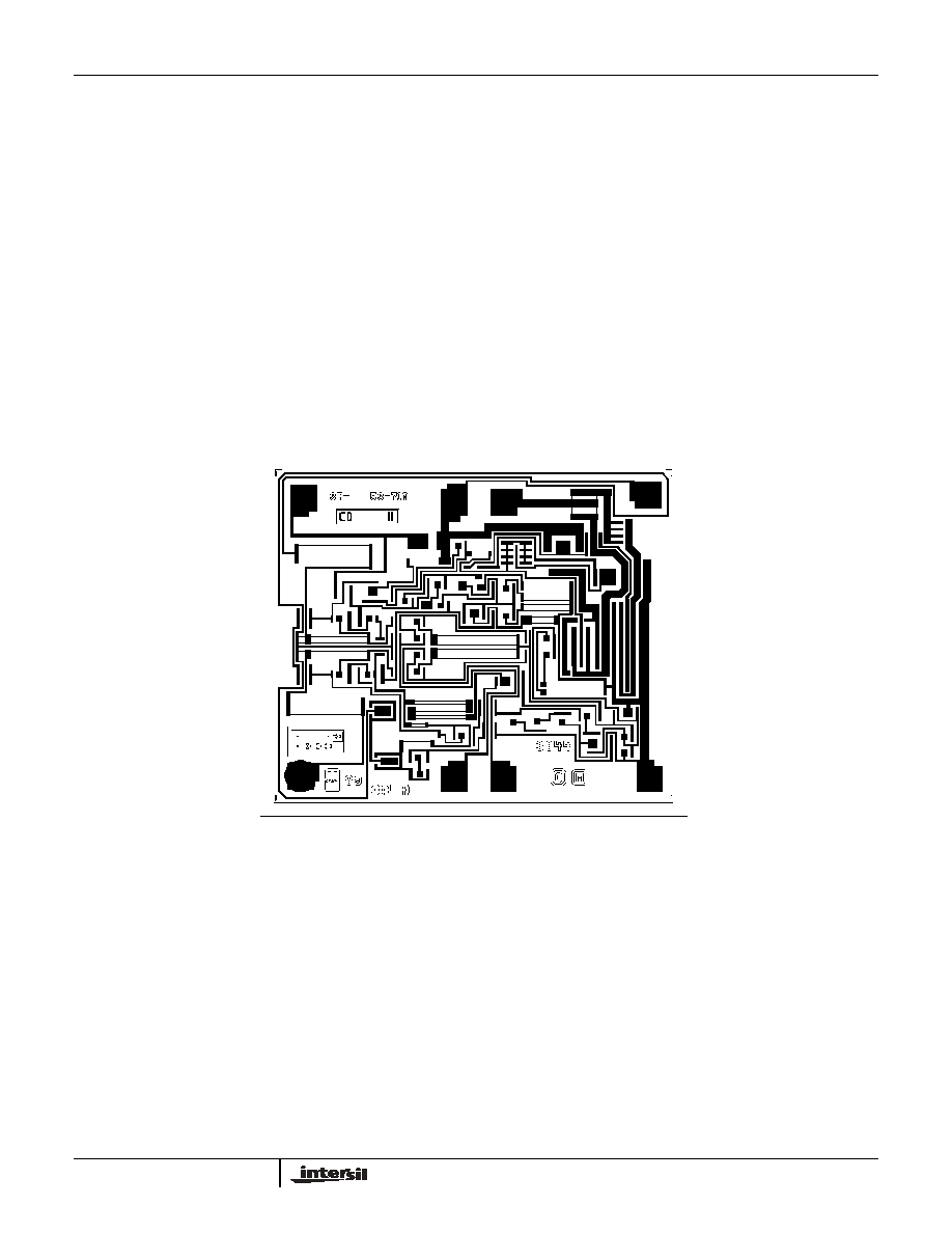
Metallization Mask Layout
HA-2529
COMP
V+
OUT
BAL
BAL
-IN
+IN
V-
HA-2529