1
HA-2600, HA-2605
12MHz, High Input Impedance Operational
Amplifiers
HA-2600/2605 are internally compensated bipolar
operational amplifiers that feature very high input impedance
(500M
, HA-2600) coupled with wideband AC performance.
The high resistance of the input stage is complemented by
low offset voltage (0.5mV, HA-2600) and low bias and offset
current (1nA, HA-2600) to facilitate accurate signal
processing. Input offset can be reduced further by means of
an external nulling potentiometer. 12MHz unity gain-
bandwidth, 7V/
µ
s slew rate and 150kV/V open-loop gain
enables HA-2600/2605 to perform high-gain amplification of
fast, wideband signals. These dynamic characteristics,
coupled with fast settling times, make these amplifiers ideally
suited to pulse amplification designs as well as high
frequency (e.g. video) applications. The frequency response
of the amplifier can be tailored to exact design requirements
by means of an external bandwidth control capacitor.
In addition to its application in pulse and video amplifier
designs, HA-2600/2605 are particularly suited to other high
performance designs such as high-gain low distortion audio
amplifiers, high-Q and wideband active filters and high-
speed comparators. For more information, please refer to
Application Note AN515.
The HA-2600 is offered as /883 Military Grade; product and
data sheet are available upon request.
Features
∑ Bandwidth. . . . . . . . . . . . . . . . . . . . . . . . . . . . . . . . 12MHz
∑ High Input Impedance . . . . . . . . . . . . . . . . . . . . . 500M
∑ Low Input Bias Current . . . . . . . . . . . . . . . . . . . . . . . . 1nA
∑ Low Input Offset Current . . . . . . . . . . . . . . . . . . . . . . 1nA
∑ Low Input Offset Voltage . . . . . . . . . . . . . . . . . . . . 0.5mV
∑ High Gain . . . . . . . . . . . . . . . . . . . . . . . . . . . . . . 150kV/V
∑ Slew Rate . . . . . . . . . . . . . . . . . . . . . . . . . . . . . . . . . 7V/
µ
s
∑ Output Short Circuit Protection
∑ Unity Gain Stable
Applications
∑ Video Amplifier
∑ Pulse Amplifier
∑ Audio Amplifiers and Filters
∑ High-Q Active Filters
∑ High-Speed Comparators
∑ Low Distortion Oscillators
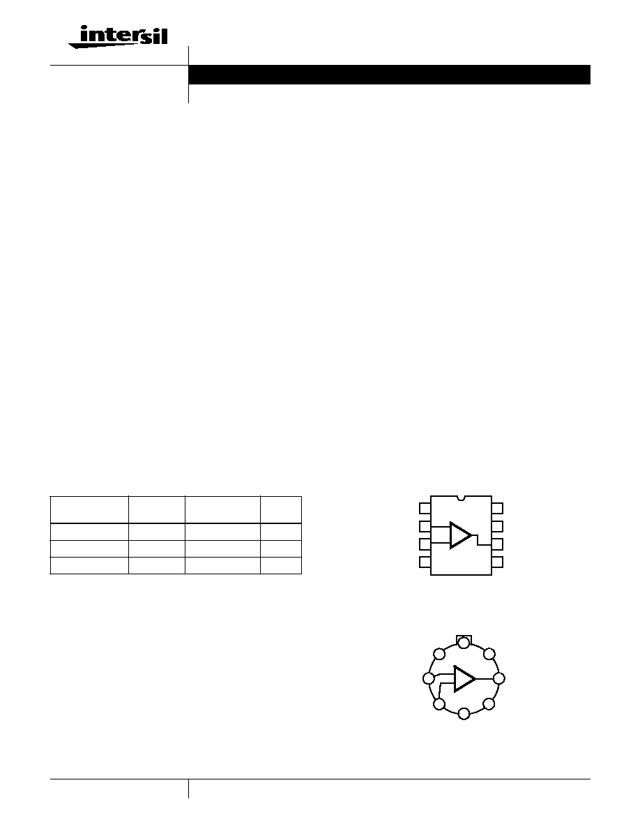
Pinouts
HA-2605
(PDIP)
TOP VIEW
HA-2600/05
(METAL CAN)
TOP VIEW
Ordering Information
PART NUMBER
TEMP.
RANGE (
o
C)
PACKAGE
PKG.
NO.
HA2-2600-2
-55 to 125
8 Pin Metal Can
T8.C
HA2-2605-5
0 to 75
8 Pin Metal Can
T8.C
HA3-2605-5
0 to 75
8 Ld PDIP
E8.3
1
2
3
4
8
7
6
5
+
BAL
-IN
+IN
V-
COMP
V+
OUT
BAL
-
COMP
OUT
-IN
BAL
+IN
V+
BAL
2
4
6
1
3
7
5
8
+
V-
-
September 1998
File Number
2902.3
CAUTION: These devices are sensitive to electrostatic discharge; follow proper IC Handling Procedures.
1-888-INTERSIL or 321-724-7143
|
Copyright
©
Intersil Corporation 1999
2
Absolute Maximum Ratings
Thermal Information
Supply Voltage Between V+ and V- Terminals . . . . . . . . . . . . . 45V
Differential Input Voltage . . . . . . . . . . . . . . . . . . . . . . . . . . . . . . 12V
Peak Output Current . . . . . . . . . . . . . . . Full Short Circuit Protection
Operating Conditions
Temperature Range
HA-2600-2 . . . . . . . . . . . . . . . . . . . . . . . . . . . . . . -55
o
C to 125
o
C
HA-2605-5 . . . . . . . . . . . . . . . . . . . . . . . . . . . . . . . . 0
o
C to 75
o
C
Thermal Resistance (Typical, Note 1)
JA
(
o
C/W)
JC
(
o
C/W)
Metal Can Package . . . . . . . . . . . . . . .
165
80
PDIP Package . . . . . . . . . . . . . . . . . . .
96
N/A
Maximum Junction Temperature (Hermetic Package) . . . . . . . .175
o
C
Maximum Junction Temperature (Plastic Package) . . . . . . . .150
o
C
Maximum Storage Temperature Range . . . . . . . . . . -65
o
C to 150
o
C
Maximum Lead Temperature (Soldering 10s) . . . . . . . . . . . . 300
o
C
CAUTION: Stresses above those listed in "Absolute Maximum Ratings" may cause permanent damage to the device. This is a stress only rating and operation of the
device at these or any other conditions above those indicated in the operational sections of this specification is not implied.
NOTE:
1.
JA
is measured with the component mounted on an evaluation PC board in free air.
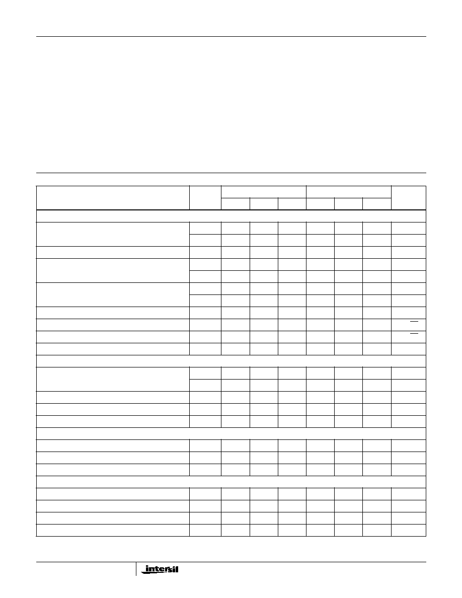
Electrical Specifications
V
SUPPLY
=
±
15V, Unless Otherwise Specified
PARAMETER
TEMP.
(
o
C)
HA-2600-2
HA-2605-5
UNITS
MIN
TYP
MAX
MIN
TYP
MAX
INPUT CHARACTERISTICS
Offset Voltage
25
-
0.5
4
-
3
5
mV
Full
-
2
6
-
-
7
mV
Average Offset Voltage Drift
Full
-
5
-
-
5
-
µ
V/
o
C
Bias Current
25
-
1
10
-
5
25
nA
Full
-
10
30
-
-
40
nA
Offset Current
25
-
1
10
-
5
25
nA
Full
-
5
30
-
-
40
nA
Differential Input Resistance (Note 12)
25
100
500
-
40
300
-
M
Input Noise Voltage Density (f = 1kHz)
25
-
11
-
-
11
-
nV/
Hz
Input Noise Current Density (f = 1kHz)
25
-
0.16
-
-
0.16
-
pA/
Hz
Common Mode Range
Full
±
11
±
12
-
±
11
±
12
-
V
TRANSFER CHARACTERISTICS
Large Signal Voltage Gain (Notes 3, 6)
25
100
150
-
80
150
-
kV/V
Full
70
-
-
70
-
-
kV/V
Common Mode Rejection Ratio (Note 4)
Full
80
100
-
74
100
-
dB
Minimum Stable Gain
25
1
-
-
1
-
-
V/V
Gain Bandwidth Product (Note 5)
25
-
12
-
-
12
-
MHz
OUTPUT CHARACTERISTICS
Output Voltage Swing (Note 3)
Full
±
10
±
12
-
±
10
±
12
-
V
Output Current (Note 6)
25
±
15
±
22
-
±
10
±
18
-
mA
Full Power Bandwidth (Notes 6, 13)
25
50
75
-
50
75
-
kHz
TRANSIENT RESPONSE (Note 10)
Rise Time (Notes 3, 7, 8, 9)
25
-
30
60
-
30
60
ns
Overshoot (Notes 3, 7, 8, 9)
25
-
25
40
-
25
40
%
Slew Rate (Notes 3, 7, 9, 14)
25
±
4
±
7
-
±
4
±
7
-
V/
µ
s
Settling Time (Notes 3, 7, 15)
25
-
1.5
-
-
1.5
-
µ
s
HA-2600, HA-2605
3
POWER SUPPLY CHARACTERISTICS
Supply Current
25
-
3
3.7
-
3
4
mA
Power Supply Rejection Ratio (Note 11)
Full
80
90
-
74
90
-
dB
NOTES:
2. Typical and minimum specifications for -9 are identical to those of -5. All maximum specifications for -9 are identical to those of -5 except for Full
Temperature Bias and Offset Currents, which are 70nA Max.
3. R
L
= 2k
.
4. V
CM
=
±
10V.
5. V
OUT
< 90mV.
6. V
OUT
=
±
10V.
7. C
L
= 100pF.
8. V
OUT
=
±
200mV.
9. A
V
= +1.
10. See Transient Response Test Circuits and Waveforms.
11.
V
S
=
±
5V.
12. This parameter value guaranteed by design calculations.
13. Full Power Bandwidth guaranteed by slew rate measurement:
.
14. V
OUT
=
±
5V
15. Settling time is characterized at A
V
= -1 to 0.1% of a 10V step.
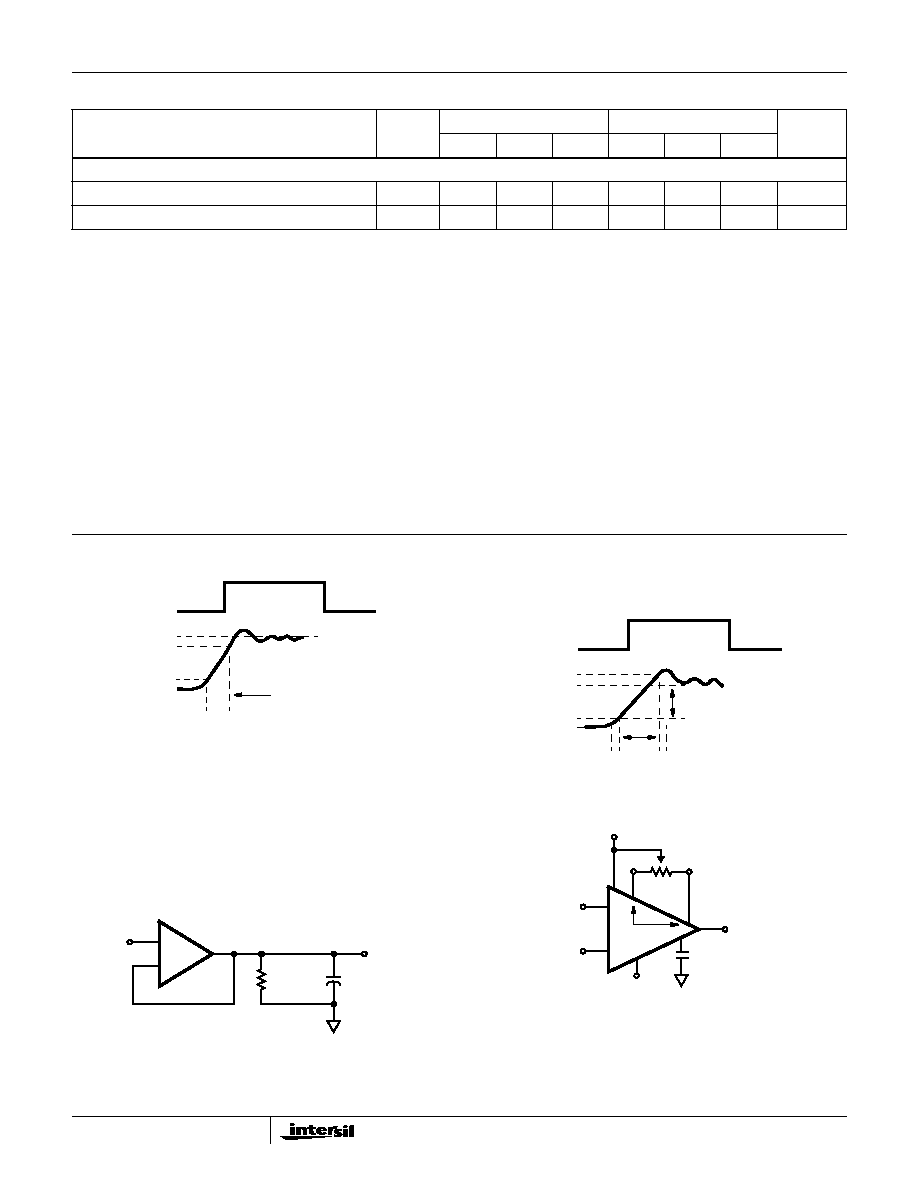
Test Circuits and Waveforms
FIGURE 1. TRANSIENT RESPONSE
FIGURE 2. SLEW RATE
FIGURE 3. SLEW RATE AND TRANSIENT RESPONSE TEST
CIRCUIT
FIGURE 4. SUGGESTED V
OS
ADJUSTMENT AND
COMPENSATION HOOK UP
Electrical Specifications
V
SUPPLY
=
±
15V, Unless Otherwise Specified (Continued)
PARAMETER
TEMP.
(
o
C)
HA-2600-2
HA-2605-5
UNITS
MIN
TYP
MAX
MIN
TYP
MAX
FPBW
Slew Rate
2
V
PEAK
---------------------------
=
INPUT
0V
±
200mV
90%
OUTPUT
10%
0V
RISE TIME
±
200mV
NOTE: Measured on both positive and negative transitions from
0V to +200mV and 0V to -200mV at the output.
INPUT
+5V
-5V
+5V
90%
OUTPUT
10%
-5V
SLEW RATE
=
V/
t
t
V
+
-
OUT
IN
2k
100pF
OUT
IN
BAL
V-
V+
100k
COMP
C
C
R
T
NOTE: Tested offset adjustment range is |V
OS
+ 1mV| minimum
referred to output. Typical ranges are
±
10mV with R
T
= 100k
.
HA-2600, HA-2605
4
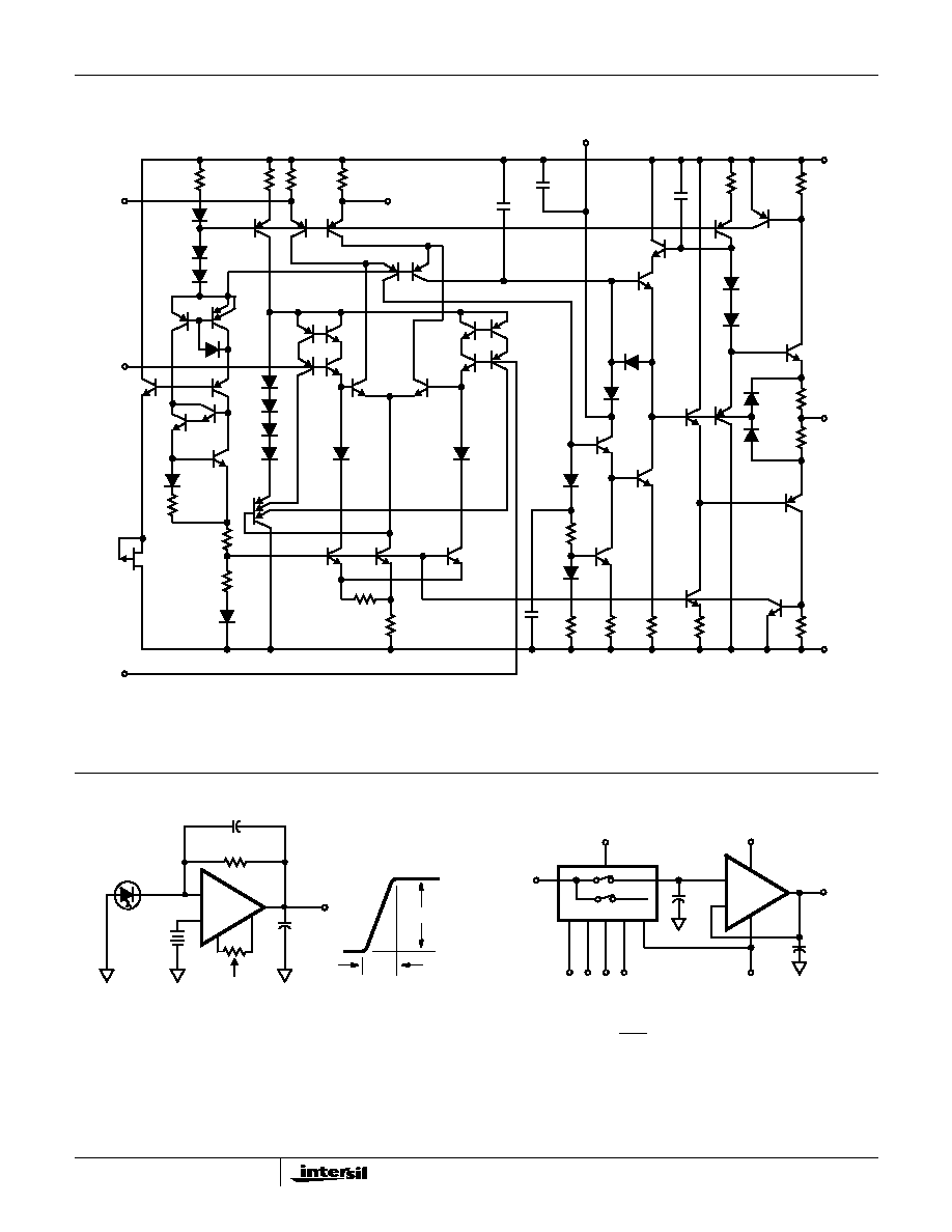
Schematic Diagram
BAL
R
1
1K
R
2
4.18K
R
3
1.56K
R
4
1.56K
Q
1
Q
3
Q
4
Q
5
Q
6
Q
7
Q
11
+INPUT
Q
8
Q
13
Q
16
Q
30
Q
29
Q
31
Q
28
Q
26
Q
25
Q
9
Q
10
Q
17
Q
18
Q
27
Q
12
Q
15
Q
2
Q
40
Q
38
Q
37
Q
24
Q
19
R
7
1.35
R
19
2.5K
R
P1
BAL
C
2
9pF
R
5
600
R
6
15
V+
Q
41
Q
42
Q
60
Q
61
Q
59
Q
58
Q
57
Q
55
Q
54
Q
43
Q
44
Q
45
Q
46
Q
47
COMPENSATION
OUT
R
18
30
R
17
30
Q
52
Q
51
R
11
4.0K
Q
49
Q
50
C
1
16pF
R
12
1.6K
R
13
1.6K
R
14
2.1K
Q
22
Q
23
R
9
4.5K
R
10
2.0K
Q
21
Q
48
R
15
800
Q
36
Q
35
Q
32
Q
33
Q
56
Q
53
R
16
15
V-
Q
20
R
8
1K
-INPUT
Q
39
C
3
16pF
C
4
4pF
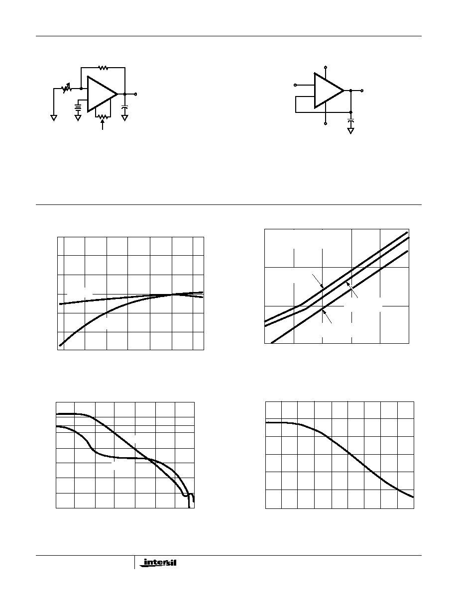
Typical Applications
NOTE: A small load capacitance is recommended in all applications where practical to prevent possible high frequency oscillations resulting from
external wiring parasitics. Capacitance up to 100pF has negligible effect on the bandwidth or slew rate.
FIGURE 5. PHOTO CURRENT TO VOLTAGE CONVERTER
FIGURE 6. SAMPLE AND HOLD
50pF (NOTE)
6V
V+
5pF
I
B
= 1nA
+
+
BAL
HA-2600
R = 40k
SILICON PHOTO
DIODE
I
P
= 50
µ
A
+6V
+2V
1
µ
s
V
O
= -R(I
P
±
I
B
)
-
FEATURES:
1. Constant cell voltage.
2. Minimum bias current error.
+5V
+15V
IN
DIGITAL CONTROL
OUT
50pF (NOTE)
C
MULTIPLEXER
+
-15V
HA-2600
DRIFT RATE =
I
BIAS
C
If C = 1000pF
Then DRIFT = 0.01V/
µ
s (Max)
-
HA-2600, HA-2605
5
NOTE: A small load capacitance is recommended in all applications where practical to prevent possible high frequency oscillations resulting from
external wiring parasitics. Capacitance up to 100pF has negligible effect on the bandwidth or slew rate.
FIGURE 7. REFERENCE VOLTAGE AMPLIFIER
FIGURE 8. VOLTAGE FOLLOWER
Typical Performance Curves
V
S
=
±
15V, T
A
= 25
o
C, Unless Otherwise Specified
FIGURE 9. INPUT BIAS CURRENT AND OFFSET CURRENT
vs TEMPERATURE
FIGURE 10. BROADBAND NOISE CHARACTERISTICS
FIGURE 11. OPEN LOOP FREQUENCY RESPONSE
FIGURE 12. INPUT IMPEDANCE vs TEMPERATURE (100Hz)
Typical Applications
(Continued)
R
1
R
2
V+
50pF (NOTE)
BAL
I
BIAS
V
REF
V
O
1
R
2
R
1
-------
V
REF
+
=
+
HA-2600
-
FEATURES:
1. Minimum bias current in reference cell.
2. Short Circuit Protection.
+15V
IN
OUT
50pF (NOTE)
+
-15V
HA-2600
-
FEATURES
1. Z
IN
= 10
12
(Min).
2. Z
OUT
= 0.01
(Max), B.W. = 12MHz (Typ).
3. Slew Rate = 4V/
µ
s (Min), Output Swing =
±
10V (Min) to 50kHz.
15
10
5
0
-5
-10
-15
-50
-25
0
25
50
75
100 125
CURRENT (nA)
TEMPERATURE (
o
C)
BIAS
OFFSET
100
10
1
0.1
100Hz
1kHz
10kHz
100kHz
1MHz
EQ
UIV
ALENT INPUT NOISE (
µ
V)
10MHz
UPPER 3dB FREQUENCY
(LOWER 3dB FREQUENCY = 10Hz)
10k
SOURCE
0
SOURCE
THERMAL NOISE
EQUIVALENT INPUT
NOISE vs BANDWIDTH
OF 10K RESISTOR
RESISTANCE
RESISTANCE
120
80
20
-20
10Hz
OPEN LOOP V
O
L
T
A
GE GAIN (dB)
FREQUENCY
100
60
40
0
100Hz
1kHz
10kHz 100kHz
1MHz
10MHz 100MHz
GAIN
PHASE
0
100
20
60
180
140
PHASE ANGLE (DEGREES)
TEMPERATURE (
o
C)
0
-35
5
45
105
125
IMPED
ANCE (M
)
1000
800
600
400
200
-55
25
-15
65
85
HA-2600, HA-2605